Unit - 1
Semiconductor Devices and Applications
Q1) Give a brief introduction on P-N Junction Diode.
A1)
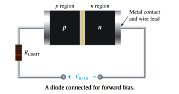
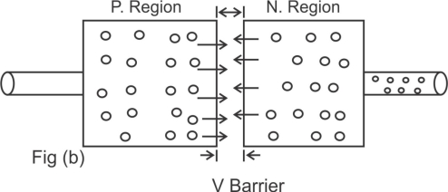
- A Forward biased showing the flow of majority carriers and the voltage due to the barrier potential across the depletion region-
- To bias a diode apply d,cvtg across it .
- Forward bias is the condition that allows current through the PN junction.
- Negative side of VBIAS is connected to the N -region of the diode and the positive side is connected to the P- region.
- A selected requirement is that the bias voltage VBIAS must be greater than the barrier potential.
- Because of like charges repel, the negative side of the bias voltage source pushes the free electrons , which are the majority carriers in the N-region towards the PN junction .the flow of free is called Electron Current.
- The –Veside of the source also provide a continues flow of electrons through the external connection (conductor).
- Into the N-region as show in fig-B
- The bias voltage source imparts sufficient energy to the free electrons for them to overcome the barrier potential of the depletion region and move on through into the 'p' region once in the P-region. These conduction electrons have lost enough energy to immediately combine with holes in the valence band.
- Now the e- are in the valance band in the P-region simply because they have lost too much energy overcoming the barrier potential to remain in the conduction band. Since unlike charge attract, the positive side of the bias voltage source attracts the valence electrons toward the left end of the region.
- The hole in the P-region provide the medium or "Pathway" for these valence electrons to move through the P-region.
- The holes which are the majority carriers in the P-region, effectively (not actually) move to the right toward the junction as shown in fig-B.
- The defective flow of holes is called the hole current.
- As from Fig-B hole current as the flow of valence electrons through the P-region with the holes providing the only means for these electrons to flow.
- As the electrons flow out of the P-region through the external connection and to the positive side of the bias in the P-region at the same time these electrons become conduction electrons in the mater conductor.
- To these is a continues availability of holes effectively moving towards the PN junction stream of electrons as they come across the junction in to the P-region.
The effect of forward bias on the depletion region:-
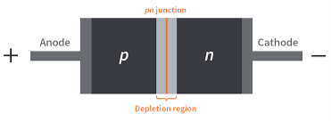

Depletion Region
- Forward bias narrows the depletion region & produce a vtg drop across pn junction equal to the barrier potential.
- As more electrons flow into the depletion region , the number of positive ions is reduce . As more notes effectively flow into the depletion region on the other side of the pnjunction ,the number of -ve ions is reduce this reduction in positive & -ve ions during forward bias causes the depletion region to narrow.
REVERSE BIAS:-
Reverse bias is the condition the essentially prevents current through the diode.
V BIAS
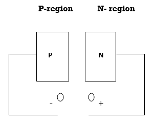
A Diode connected for Reverse Biased-
- Because unlike charges attract the positive side of the bia voltage source pulls the free election, which are the majority carriers in the N-region away from the PN junction.
- AS the election flow towards the positive side of the voltage source additional positive ions are created
- This results in a widening of the depletion region and a depletion of majority carriers.
- The diode during the short transition time immediately after reverse bias vtg is applied-
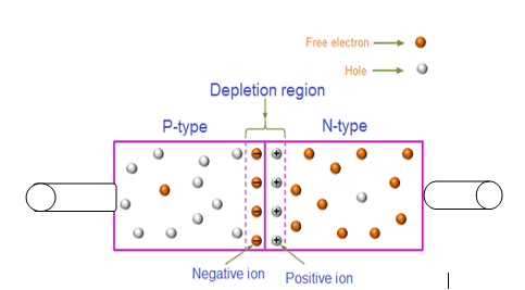
- In the P-region electrons from the negative side of the vtg source enter as valence electron and move from hole to hole toward the depletion region where the creators additional -ve ions.
- This results in a widening of the depletion region and a depletion of majority carriers
- As the depletion region widens the availability of majority carriers decreases
- As more of the N & P regions become depleted of majority carriers, the electric field between the positive and -ve ions increase in strength the depletion region equals the bios vtg .this point the transition current essentially ceases except for a small reverse current that can usually be neglected.
Q2) What do you understand by Half Wave rectifier?
A2)
1) Due to the unidirectional current flow through the transformer there is a possibility of core saturation to avoid this transformer size must be increased.
2) Ripple factor is high.
3) Low rectification effecting.
4) Law TUF.
5) Law D.C O/P VTG & current.
6) Large filter component are required.
ADVANTAGES:-
1) Simple Construction.
2) Component required less.
3) Small size.
APPLICATION:-
Walkman, law cost power supply.
TRANSFORMER UTILISATION FACTOR (TUF):-It indicates how well the ilp transformer is being utilized
TUF= DC O/P Power / AC power rating of the transformer

Q3) Write a short note on Full Wave Rectifier?
A3)
1) A centre tapped rectifier is a type of full wave rectifier that uses two diode connected to the secondary of a centre tapped transformer.
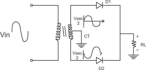
Center tapped full wave rectifier operation:-
I) During positive half cycle of i/p ac supply.
Diagram

D1.Is in forward biased & D2 is in reverse biased.
II)During -ve half cycle.

D1 Reverse biased
D2 Forward biased
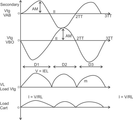
ADVANTAGES
1) law ripple factor as Compared to HKR.
2)Better rectification efficiency.
3) Better TUF.
4)Higher value of average load vtg& avg load crt.
5)No possibility of transformer core saturation.
DISADVANTAGES
PIV of diode is 2vm , more size costly.
APPLICATION
I) Battery charges.
2)power supply at laboratory, high current, electronic ckt.
Q4) Explain the work of Capacitor filter?
A4)
Being that capacitors have offer very high resistance to low frequency signals and low resistance to high frequency signals, it acts as a high pass filter, which is a filter which passes high frequency signals and blocks low frequency signals.
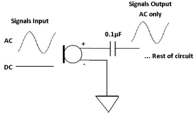
Many times in a circuit, both DC and AC signals need to be both be used in a circuit, at least at a certain stage of the circuit. However, at another stage, in the circuit, we may only want AC signals and the DC taken out. An example of such a circuit is a microphone circuit. We need DC as input to the microphone for it to be able to be powered on and we need AC as input, which represents the voice signal or music, etc. which we want the microphone to record.
We use a capacitor to filter out the DC signal.
We do this by placing the capacitor in series. In this configuration, which is the circuit you see below, this is a capacitive high-pass filter. Low frequency, or DC, signals will be blocked.
Usually, a 0.1µF ceramic capacitor, or value around that range, is placed after the signal that contains both DC and AC signals. And this capacitor filters out the DC component so that only AC goes through.
Q5) Explain the working process of Zener diode and its characteristics?
A5)
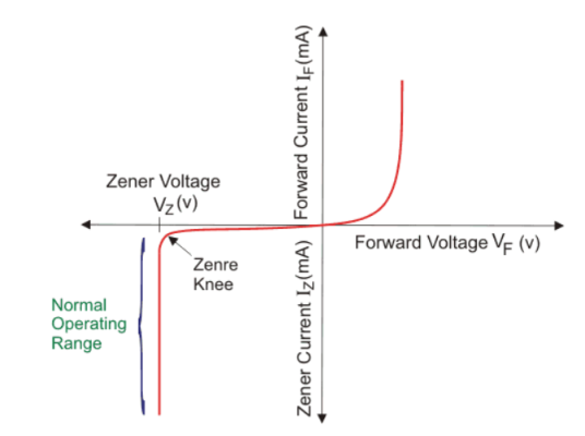
- Zener diode is a special type of p-n junction semiconductor diode in this diode the reverse breakdown voltage is adjusted precisely between 3v to 200v.
- Its applications are based on this principle hence Zener diode is called as a breakdown diode.
- The doping level of the imparity added to manufacture the zener diode is controlled in order to adjust the precise value of breakdown voltage.
PRINCIPLE OF OPERATION: - A zener diode can be forward biased or reverses biased. Its operation in the forward biased mode is same as that of a p-n junction diode but its operation in the reverse biased mode is sustainably deferent.

Q6) Write a brief description on Zener diode as voltage regulator?
A6)
Zener Diodes can be used to produce a stabilized voltage output with low ripple under varying load current conditions. By passing a small current through the diode from a voltage source, via a suitable current limiting resistor (RS), the zener diode will conduct sufficient current to maintain a voltage drop of Vout.
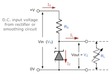
Resistor, RS is connected in series with the zener diode to limit the current flow through the diode with the voltage source, VS being connected across the combination. The stabilized output voltage Vout is taken from across the zener diode.
The zener diode is connected with its cathode terminal connected to the positive rail of the DC supply so it is reverse biased and will be operating in its breakdown condition. Resistor RS is selected so to limit the maximum current flowing in the circuit.
With no load connected to the circuit, the load current will be zero, ( IL = 0 ), and all the circuit current passes through the zener diode which in turn dissipates its maximum power. Also a small value of the series resistor RS will result in a greater diode current when the load resistance RL is connected and large as this will increase the power dissipation requirement of the diode so care must be taken when selecting the appropriate value of series resistance so that the zener’s maximum power rating is not exceeded under this no-load or high-impedance condition.
The load is connected in parallel with the zener diode, so the voltage across RL is always the same as the zener voltage, ( VR = VZ ). There is a minimum zener current for which the stabilization of the voltage is effective and the zener current must stay above this value operating under load within its breakdown region at all times. The upper limit of current is of course dependent upon the power rating of the device. The supply voltage VS must be greater than VZ.
Q7) A 5.0V stabilized power supply is required to be produced from a 12V DC power supply input source. The maximum power rating PZ of the zener diode is 2W. Using the zener regulator circuit above calculate:
a). The maximum current flowing through the zener diode.
b). The minimum value of the series resistor, RS
c). The load current IL if a load resistor of 1kΩ is connected across the zener diode.
d). The zener current IZ at full load.
A7)
a). The maximum current flowing through the zener diode.
Maximum current = Watts/ Voltage =2W/5V =400mA
b). The minimum value of the series resistor, RS
 = 17.5 Ω
c). The load current IL if a load resistor of 1kΩ is connected across the zener diode.

d). The zener current IZ at full load.
Iz =Is -Il =440mA – 5mA = 395mA
Q8) What do you understand by Regulated power supply IC based on 78XX and 79XX series?
A8)
There are two types of voltage regulators −
- Fixed voltage regulator
- Adjustable voltage regulator
Fixed voltage regulator
A fixed voltage regulator produces a fixed DC output voltage, which is either positive or negative. In other words, some fixed voltage regulators produce positive fixed DC voltage values, while others produce negative fixed DC voltage values.
78xx voltage regulator ICs produce positive fixed DC voltage values, whereas, 79xx voltage regulator ICs produce negative fixed DC voltage values.
The following points are to be noted while working with 78xx and 79xx voltage regulator ICs −
- “xx” corresponds to a two-digit number and represents the amount (magnitude) of voltage that voltage regulator IC produces.
- Both 78xx and 79xx voltage regulator ICs have 3 pins each and the third pin is used for collecting the output from them.
- The purpose of the first and second pins of these two types of ICs is different −
- The first and second pins of 78xx voltage regulator ICs are used for connecting the input and ground respectively.
- The first and second pins of 79xx voltage regulator ICs are used for connecting the ground and input respectively.
Adjustable voltage regulator
An adjustable voltage regulator produces a DC output voltage, which can be adjusted to any other value of certain voltage range. Hence, adjustable voltage regulator is also called as a variable voltage regulator.
The DC output voltage value of an adjustable voltage regulator can be either positive or negative.
Q9) What do you mean by BJT? Explain its work?
A9)
BJT:-The BJT is constructed with the three draped semiconductors region’s separate by two Pn junctions as shown below
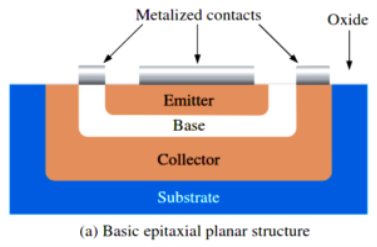
-Basic epitaxial planner structures.
-Three terminal with region’s are called emitter, base and collector.
-The physical representation of the two types of BJT’s,
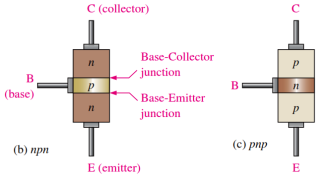
One type consists between two regions separated by a P region (npn) and other type consists of two p regions separated by an n region (pnp).
-The Pn junction joining the base region and the emitter region is called the base emitter junction.
-The Pn junction joining the base region and the collector region is called the base collector junction.
-The base region is lightly doped and very thin compared to the heavily doped emitter and the moderately doped collector regions.
Base Transistor Operation:-
In order for the transistor to operate properly as an amplifier the two pn junction must be correctly biased with the external D.C vtg.
-The next figure shows the proper bias arrangement for both the npn and pnp transistors for active operation as an amplifier.
-In both the cases the base emitter
(BE) junction is forward biased & the base collector junction (BC) junction is reverse biased
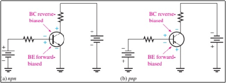
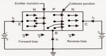
- As from above figure consider n-p-n transistor. The forward bias from base to emitter narrow’s the BE depletion region and the reverse bias from base to collector widens the BC depletion region shown in figure.
- The heavily doped N-TYPE emitter region is full with conduction band(frep) electron’s that easily diffuse through the forward biased BE junction into the p-type base region where they become minority carrier’s same as forward biased diode region
- The base region is lightly doped & very thin so that it has a very limited number of holes.
- Those only a small percentage of all the e-flowing the BE junction can combine with the available holes in the base.
- The relatively few recombined flow out of the base lead as valance electrons, forming as small base current.
- Most of the e flowing from the emitter into the thin lightly dooped base region do not recombine but diffuse into the BC depletion region.
- The BC depletion region diffuse e is being pulled across the reverse biased BC junction by the attraction of the collector supply vtg.
- The electrons now move through the collector region, out through the collector lead into the +ve terminal of the collector vtg source. This forms the collector electrons current.
- The collector current is much larger than the base current.
- This is the reason transistor exhibit current gain.
Q10) Explain the working process of BJT as a single stage CE amplifier?
A10)
Common Emitter (CE) configuration
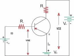
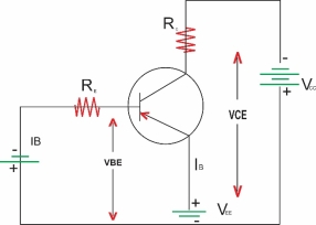
The important points about the CE
Configurations are as follows: the emitter acts as a common terminal between I/p and output. The /p Vtg. Is called between base and emitter
Hence VBE is the I/p Vtg. And IB is the input current.
The O/p is taken between the collector and emitter. There for VCE is the O/p Vtg. And IC is the O/p current.
In order to operate the transistor in its active region the base emitter (BE) junction is forward biased and collector base junction is reverse biased.
- Current relations in CE Configuration:
IE = IC + IB
Where IC =  d.c.IE + ICBO
Rearrange this eqn to get
IC – ICBO =  d.c.IE
 -
-  = IE = IC + IB
 ] = IB -
IC  ] = IB +
 ] +
] + 
- Current gain
 : as
: as  is the ration of o/p current TC and I/p current IB it called common emitter current amplification factor or simply current gain. Thus transistor acts as current amplifier.
The value of  is match higher than
 =
= 
 =
=  =
=  =
= 
IC =  IB +
IB +  …….. I
But  =
= 
 1 +
1 +  =
=  + 1
+ 1
1 +  =
= 
 1 +
1 +  =
= 
Put in eqn I
IC =  IB + (1+
 ICBO above eqn can be expressed as
IC =  IB + ICEO
Where ICEO is the reverse saturation current for the CE configuration which is given by
ICEO = (1+  ) ICBO
- Reverse leakage current :
The Reverse leakage current of a transistor operating
In the LE configuration is denoted by
ICEO = (1 +  ) ICBO
As the value of 
- Match greater than 1 ICEO>>>> ICBO
- As IC =

Put IB = 0
 IC = (1 +
The Reverse leakage current (ICEO)
Increases with increase in the temperature this current flows in the same direction as that of IC there for the collector current IC will increase with increase in temperature even when IB is constant
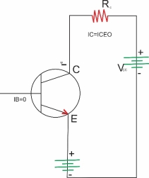
This is called as thermal instability so in CE configuration thermal stabilizing CKT must be included.
- Relation between IC and IB (Current gain
 )
)
We know that
IC 
Though ICEO is large it is much smaller as compared to . Therefor the eqn for IC gets modified as
 C =
C = 

- Relation betn
 &
& :
:
We know that
 but
but
 =
=  =
= 
 =
= 
Similarly we can obtain the expression for  d.c in terms of
  as follows
 d.c =
d.c =  but
but 
=
Multiply & divide numerator & denominator for by IE
 d.c =
d.c = 
 d.c =
d.c = 
 =
= 
- Impact characteristics:
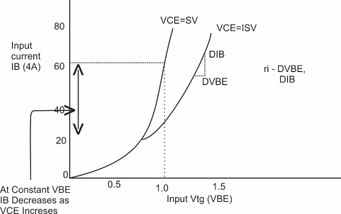
The value of dynamic input resistance ri is low for the CE configuration but it is not as low as that of CE configuration
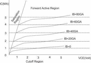
- Cutoff region: Both the BE & CB junctions are reverse biased to operate the transistor in cutoff region. The base current IB = 0 & the collector current is equal to the reverse leakage ICEO. The region below the characteristics for
IB = 0 is cutoff region.
- Active region : the BE emitter junction is forward biased CB junction is reverse biased to operate the transistor in the active region
The collector current IC increases slightly with increase in the vtg.VCE. However the collector current is largely dependent on the base current IB
At fixed value of VCE if IB is increased then it will cause IC to increase substantially.
This is because IC = BIB this relation is true only for the active region of operation.
- Saturation region : the BE junction as well as the collector junction must be forward biased to operate the transistor in its saturation region
- Dynamic o/p resistance
 / constant IB