Unit 2
Q1) How a BCD adder adds A= 0111 and B= 1000?
Sol: We are adding A(=7) and B(=8).
The value of the binary sum will be 1111(=15).
But the BCD sum will be 1 0101,
Where 1 is 0001 in binary and 5 is 0101 in binary.
Q2) How a BCD adder adds A= 0101 and B= 1001?
Sol: We are adding A(=5) and B(=9).
The value of the binary sum will be 1110(=14).
But, the BCD sum will be 1 0100,
Where 1 is 0001 in binary and 4 is 0100 in binary.
Now, let's move to the table and find out the logic when we are going to add “0110”.
We are adding “0110” (=6) only to the second half of the table because of the following conditions:
- If C’ = 1 (Satisfies 16-19)
- If S3′.S2′ = 1 (Satisfies 12-15)
- If S3′.S1′ = 1 (Satisfies 10 and 11)
So, our logic is
C' + S3'.S2' + S3'.S1' = 1
Q3) Determine the logic diagram for the logic expression obtained in Q2?
Sol:
C' + S3'.S2' + S3'.S1' = 1
Implementation :
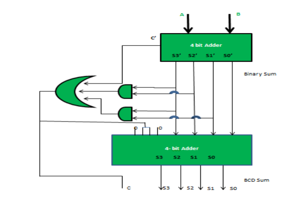
Fig: BCD adder
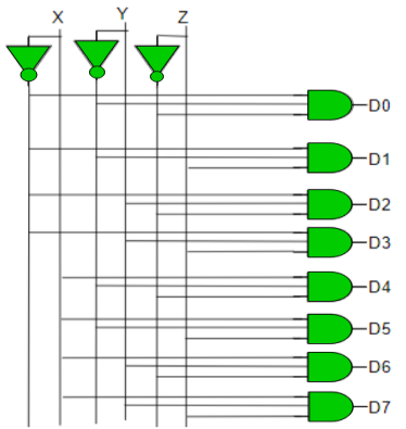
Q4) For IC 74238 draw and explain the internal circuit?
Sol: The IC 74238 is basically of a decoder.
- It works as an inverse of an encoder.
- It is a combinational circuit which converts n input lines into 2n output lines.
- Taking an example of 3-to-8 line decoder.
X | Y | Z | D0 | D1 | D2 | D3 | D4 | D5 | D6 | D7 |
0 | 0 | 0 | 1 | 0 | 0 | 0 | 0 | 0 | 0 | 0 |
0 | 0 | 1 | 0 | 1 | 0 | 0 | 0 | 0 | 0 | 0 |
0 | 1 | 0 | 0 | 0 | 1 | 0 | 0 | 0 | 0 | 0 |
0 | 1 | 1 | 0 | 0 | 0 | 1 | 0 | 0 | 0 | 0 |
1 | 0 | 0 | 0 | 0 | 0 | 0 | 1 | 0 | 0 | 0 |
1 | 0 | 1 | 0 | 0 | 0 | 0 | 0 | 1 | 0 | 0 |
1 | 1 | 0 | 0 | 0 | 0 | 0 | 0 | 0 | 1 | 0 |
1 | 1 | 1 | 0 | 0 | 0 | 0 | 0 | 0 | 0 | 1 |
D0 is high when X = 0, Y = 0 and Z = 0. Hence,
D0 = X’ Y’ Z’
Similarly,
D1 = X’ Y’ Z
D2 = X’ Y Z’
D3 = X’ Y Z
D4 = X Y’ Z’
D5 = X Y’ Z
D6 = X Y Z’
D7 = X Y Z
Hence,
Q5) Explain implementation of Adder using IC 7483?
Sol: The 4-bit BCD adder is shown below using IC 7483. As we already know that a BCD number cannot be greater than 9. So, when the digits are added the sum should be less than 9 and with carry 0. But if the case is otherwise, then a combinational circuit is needed additionally in the circuit. This combinational circuit checks the sum if less than 9 or not, if not than correction is required. The output of the combinational circuit will be high if Cout from adder-1 is not 0.
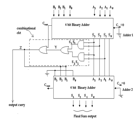
The output Y is ORed with Cout. The output Z of the combinational circuit will be high if Cout is not zero. Hence, making the bits B1 and B2 of adder-2 high. If Cout =1 then, B3B2B1B0 of adder-2 will be 0110. The sum from adder-1 is connected to adder-2 and the carry generated here is discarded.
The truth table of BCD number is shown below.
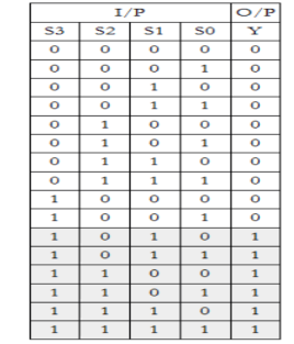
The k-map for the combinational circuit along with truth table is shown below.
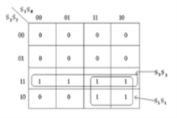
The output expression will be Y= S3S2+S3S1
Let’s consider one example addition of two BCD numbers A=0111 and B= 1001.
0111
 +1001
+1001
10000
Cout = 1
So, output Z of combinational circuit will be high i.e Z=1. The sum output of adder-1(S3-S0) =0000 is input to LSB of adder-2. As Z=1, B3B2B1B0 of adder-2 will be 0110. So, the final output from adder-2 (S3-S0) will be 0110 and carry as 1(0001).
Therefore, (0111) BCD+(1001) BCD = (00010110) BCD
Q6) How IC 7483 can work as subtractor?
Half Subtractor:
The change we need to make in the arrangement of IC 7483 to make it work as a subtractor is that the minuend is connected the way it was. We just negate the bits of subtrahend before connecting, and then add the numbers which gives the difference as output.
If A=1000 B=0110
We need to find A-B
So, we first find 2’s compliment of B = 1010
Then adding both 1000+1010= 0010 and the carry is discarded.
Q7) Explain the pin configuration of IC 7483?
Sol: The BCD adder IC 7483 is shown below. It is a 16-pin chip. The pin configuration is explained below. When two IC connected in series adds the eight bit number.
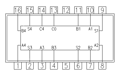
Fig: IC 7483
Pin1: A4 input
Pin2: S3 (sum output bit)
Pin3: A3 input
Pin4: B3 input
Pin5: Supply (Vcc)
Pin6: S2 (Sum output bit)
Pin7: B2 input
Pin8: A2 input
Pin9: S1 sum output bit
Pin10: A1 input
Pin11: B1 input
Pin12: Ground
Pin13: C0 input
Pin14: C4 input
Pin15: S4 output
Pin16: B4 input
Q8) Explain the logic diagram of an encoder?
- Sol: When more than one input becomes active at the same time then the input with higher priority takes precedence w.r.to the output which is generated.
- Considering a 4:2 priority encoder.
- From the truth table given below we see that when all inputs are 0, V bit is zero and outputs are not used.
- The x in the table shows the don’t care condition, i.e it can be 0 or 1.
- Here, D3 has highest priority, therefore, when D3 is high, output has to be 11.
- D0 has the lowest priority, hence the output would be 00 only when D0 is high and all the other input lines are low.
Truth Table –
D3 | D2 | D1 | D0 | X | Y | V |
0 | 0 | 0 | 0 | x | x | 0 |
0 | 0 | 0 | 1 | 0 | 0 | 1 |
0 | 0 | 1 | x | 0 | 1 | 1 |
0 | 1 | X | x | 1 | 0 | 1 |
1 | x | X | x | 1 | 1 | 1 |
Implementation –
The condition for valid bit to be 1 is when at least one of the inputs should be high. Hence,
V = D0 + D1 + D2 + D3
For X:
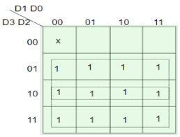
=>X=D2+D3
For Y:
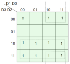
=> Y = D1 D2’ + D3
Hence, the priority 4-to-2 encoder can be realized as follows:
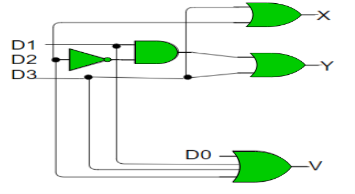
Fig: Priority encoder
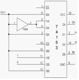
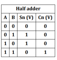
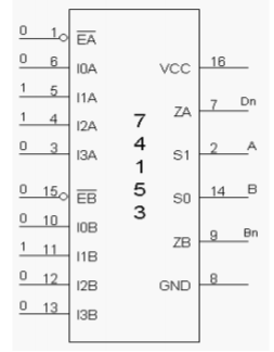
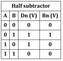
Q9) Explain implementation of half adder and half subtractor using IC 7153?
Sol: IC 74153 is a multiplexer. Here we will implement half adder, full adder, half subtractor and full subtractor.
1) The Pin 16 is connected to + Vcc.
2) Pin 8 is connected to ground.
3) The inputs are applied either to ‘A’ input or ‘B’ input.
4) If MUX ‘A’ has to be initialized, Ea is made low and if MUX ‘B’ has to be initialized, Eb is made low.
5) Based on the selection lines one of the inputs will be selected at the output and thus the truth table is verified.
6) In case of half adder using MUX, sum and carry is obtained by applying a constant input at I0a, I1a, I 2a, I 3a and I 0b, I 1b, I 2b and I3b and the corresponding values of select lines are changed as per table and the output is taken at Z0a as sum and Z0b as carry.
7) In this case, the channels A and B are kept at constant inputs according to the table and the inputs A and B are varied. Making Ea and Eb zero and the output is taken at Za, and Zb.
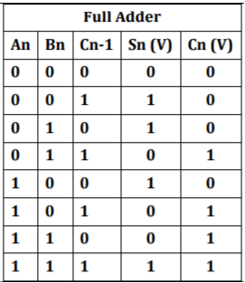
8) In full adder using MUX, the input is applied at Cn-1, An and Bn. According to the table corresponding outputs are taken at Cn and Dn.
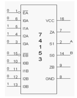
Half Subtractor:
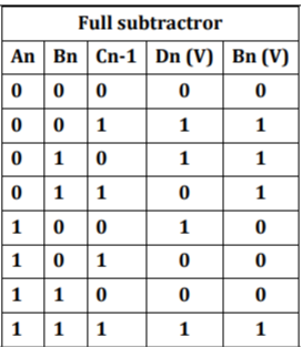
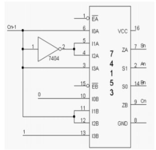
Q10) Explain the implementation of full adder and subtractor using IC 74513?
Sol: IC 74153 is a multiplexer. Here we will implement half adder, full adder, half subtractor and full subtractor.
1) The Pin 16 is connected to + Vcc.
2) Pin 8 is connected to ground.
3) The inputs are applied either to ‘A’ input or ‘B’ input.
4) If MUX ‘A’ has to be initialized, Ea is made low and if MUX ‘B’ has to be initialized, Eb is made low.
5) Based on the selection lines one of the inputs will be selected at the output and thus the truth table is verified.
6) In case of half adder using MUX, sum and carry is obtained by applying a constant input at I0a, I1a, I 2a, I 3a and I 0b, I 1b, I 2b and I3b and the corresponding values of select lines are changed as per table and the output is taken at Z0a as sum and Z0b as carry.
7) In this case, the channels A and B are kept at constant inputs according to the table and the inputs A and B are varied. Making Ea and Eb zero and the output is taken at Za, and Zb.
8) In full adder using MUX, the input is applied at Cn-1, An and Bn. According to the table corresponding outputs are taken at Cn and Dn.
Full Subtractor:
