UNIT 4
Computer Organization &Processor
- Explain in detail Organization, functions & types of computer units
- A computer organization describes the functions and design of the various units of a digital system.
- A general-purpose computer system is the best-known example of a digital system. Other examples include telephone switching exchanges, digital voltmeters, digital counters, electronic calculators and digital displays.
- Computer architecture deals with the specification of the instruction set and the hardware units that implement the instructions.
- Computer hardware consists of electronic circuits, displays, magnetic and optic storage media and also the communication facilities.
- Functional units are a part of a CPU that performs the operations and calculations called for by the computer program.
- Functional units of a computer system are parts of the CPU (Central Processing Unit) that performs the operations and calculations called for by the computer program. A computer consists of five main components namely, Input unit, Central Processing Unit, Memory unit Arithmetic & logical unit, Control unit and an Output unit.
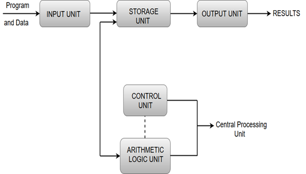
Input unit
- Input units are used by the computer to read the data. The most commonly used input devices are keyboards, mouse, joysticks, trackballs, microphones, etc.
- However, the most well-known input device is a keyboard. Whenever a key is pressed, the corresponding letter or digit is automatically translated into its corresponding binary code and transmitted over a cable to either the memory or the processor.
Central processing unit
- Central processing unit commonly known as CPU can be referred as an electronic circuitry within a computer that carries out the instructions given by a computer program by performing the basic arithmetic, logical, control and input/output (I/O) operations specified by the instructions.
Memory unit
- The Memory unit can be referred to as the storage area in which programs are kept which are running, and that contains data needed by the running programs.
- The Memory unit can be categorized in two ways namely, primary memory and secondary memory.
- It enables a processor to access running execution applications and services that are temporarily stored in a specific memory location.
- Primary storage is the fastest memory that operates at electronic speeds. Primary memory contains a large number of semiconductor storage cells, capable of storing a bit of information. The word length of a computer is between 16-64 bits.
- It is also known as the volatile form of memory, means when the computer is shut down, anything contained in RAM is lost.
- Cache memory is also a kind of memory which is used to fetch the data very soon. They are highly coupled with the processor.
- The most common examples of primary memory are RAM and ROM.
- Secondary memory is used when a large amount of data and programs have to be stored for a long-term basis.
- It is also known as the Non-volatile memory form of memory, means the data is stored permanently irrespective of shut down.
- The most common examples of secondary memory are magnetic disks, magnetic tapes, and optical disks.
Arithmetic & logical unit
- Most of all the arithmetic and logical operations of a computer are executed in the ALU (Arithmetic and Logical Unit) of the processor. It performs arithmetic operations like addition, subtraction, multiplication, division and also the logical operations like AND, OR, NOT operations.
Control unit
- The control unit is a component of a computer's central processing unit that coordinates the operation of the processor. It tells the computer's memory, arithmetic/logic unit and input and output devices how to respond to a program's instructions.
- The control unit is also known as the nerve center of a computer system.
- Let's us consider an example of addition of two operands by the instruction given as Add LOCA, RO. This instruction adds the memory location LOCA to the operand in the register RO and places the sum in the register RO. This instruction internally performs several steps.
Output Unit
- The primary function of the output unit is to send the processed results to the user. Output devices display information in a way that the user can understand.
- Output devices are pieces of equipment that are used to generate information or any other response processed by the computer. These devices display information that has been held or generated within a computer.
- The most common example of an output device is a monitor.
2. Explain Processor Organization
To understand the organization of the CPU, let us consider the requirements placed on the CPU, the things that it must do:
- Fetch instruction: The CPU reads an instruction from memory.
- Interpret instruction: The instruction is decoded to determine what action is required.
- Fetch data: The execution of an instruction may require reading data from memory or an I/O module.
- Process data: The execution of an instruction may require performing some arithmetic or logical operation on data.
- Write data: The results of an execution may require writing data to memory or an I/O module.
To do these things, it should be clear that the CPU needs to store some data temporarily. It must remember the location of the last instruction so that it can know where to get the next instruction. It needs to store instructions and data temporarily while an instruction is being executed. In other words, the CPU needs a small internal memory.
Figure is a simplified view of a CPU, indicating its connection to the rest of the system via the system bus. You will recall (Lecture 1) that the major components of the CPU are arithmetic and logic unit (ALU) and a control unit (CU). The ALU does the actual computation or processing of data. The control unit controls the movement of data and instructions into and out of the CPU and controls the operation of the ALU. In addition, the figure shows a minimal internal memory, consisting of a set of storage locations, called registers.
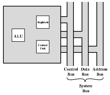
The CPU with the System Bus
Figure is a slightly more detailed view of the CPU. The data transfer and logic control paths are indicated, including an element labeled internal CPU-bus. This element is needed to transfer data between the various registers and the ALU because the ALU in fact operates only on data in the internal CPU memory.
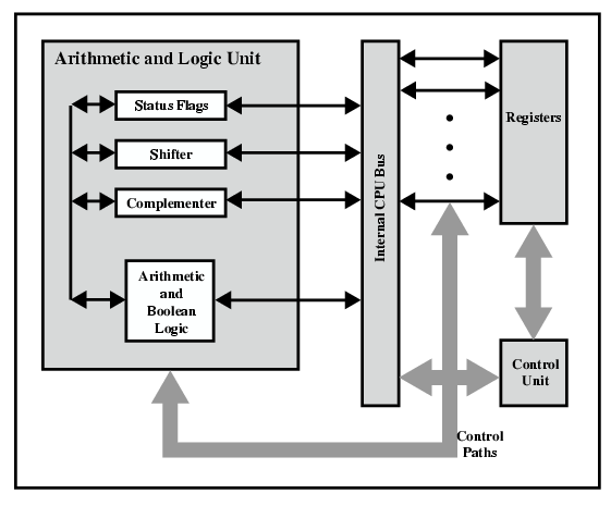
CPU Internal Structure
3. Explain Register organization
Within the CPU, there is a set of registers that function as a level of memory above main memory and cache in the hierarchy. The registers in the CPU perform two roles:
- User-visible registers: These enable the machine- or assembly-language programmer to minimize main memory references by optimizing use of registers.
- Control and status registers: These are used by the control unit to control the operation of the CPU and by privileged, operating system programs to control the execution of programs.
There is not a clean separation of registers into these two categories. For example, on some machines the program counter is user visible (e.g., Pentium), but on many it is not (e.g., PowerPC). For purposes of the following discussion, however, we will use these categories.
User-Visible Registers
A user-visible register is one that may be referenced by means of the machine language that the CPU executes. We can characterize these in the following categories:
- General purpose
- Data
- Address
- Condition codes
General-purpose registers: can be assigned to a variety of functions by the programmer. Sometimes their use within the instruction set is orthogonal to the operation. That is, any general--purpose register can contain the operand for any opcode. This provides true general-purpose register use. Often, however, there are restrictions. For example, there may be dedicated registers for floating-point and stack operations. In some cases, general-purpose registers can be used for addressing functions (e.g.. register indirect, displacement). In other cases, there is a partial or clean separation between data registers and address registers.
Data registers may be used only to hold data and cannot be employed in the calculation of an operand address.
Address registers may themselves be somewhat general purpose, or they may be devoted to a particular addressing mode. Examples include the following:
- Segment pointers: In a machine with segmented addressing, a segment register holds the address of the base of the segment. There may be multiple registers: for example, one for the operating system and one for the current process.
- Index registers: These are used for indexed addressing and may be auto indexed.
- Stack pointer: If there is user-visible stack addressing, then typically the stack is in memory and there is a dedicated register that points to the top of the slack. This allows implicit addressing; that is, push, pop, and other slack instructions need not contain an explicit stack operand.
Condition codes register (also referred to as flags): Condition codes are bits set by the CPU hardware as the result of operations. For example, an arithmetic operation may produce a positive, negative, zero, or overflow result. In addition to the result itself being stored in a register or memory, a condition code is also set. The code may subsequently be tested as part of a conditional branch operation.
Control and Status Registers
There are a variety of CPU registers that are employed to control the operation of the CPU. Most of these, on most machines, are not visible to the user. Some of them may be visible to machine instructions executed in a control or operating system mode.
Of course, different machines will have different register organizations and use different terminology. We list here a reasonably complete list of register types, with a brief description.
4. How many registers are essential to instruction execution?
Four registers are essential to instruction execution:
- Program counter (PC): Contains the address of an instruction to be fetched.
- Instruction register (IR): Contains the instruction most recently fetched.
- Memory address registers (MAR): Contains the address of a location in memory.
- Memory buffer register (MBR): Contains a word of data lo be written to memory or the word most recently read.
Typically, the CPU updates the PC after each instruction fetch so that the PC always points to the next instruction to be executed. A branch or skip instruction will also modify the contents of the PC. The fetched instruction is loaded into an IR, where the opcode and operand specifiers are analysed. Data are exchanged with memory using the MAR and MBR. In a bus-organized system, the MAR connects directly to the address bus, and the MBR connects directly to the data bus. User-visible registers, in turn, exchange data with the MBR.
The four registers just mentioned are used for the movement of data between the CPU and memory. Within the CPU, data must be presented to the ALU for processing. The ALU may have direct access to the MBR and user-visible registers. Alternatively, there may be additional buffering registers at the boundary to the ALU: these registers serve as input and output registers for the ALL and exchange data with the MBR and user-visible registers.
All CPU designs include a register or set of registers, often known as the program status word (PSW), that contain status information. The PSW typically contains condition codes plus other stains information. Common fields or flags include the following:
- Sign: Contains the sign bit of the result of the last arithmetic operation.
- Zero: Set when the result is 0.
- Carry: Set if an operation resulted in a carry (addition) into or borrow (sub-traction) out of a high-order hit. Used for multiword arithmetic operations.
- Equal: Set if a logical compare result is equality.
- Overflow: Used to indicate arithmetic overflow
- Interrupt enable/disable: Used to enable or disable interrupts.
- Supervisor: Indicates whether the CPU is executing in supervisor or user mode. Certain privileged instructions can be executed only in supervisor mode, and certain areas of memory can be accessed only in supervisor mode.
A number of other registers related to status and control might be found in a particular CPU design. In addition to the PSW, there may be a pointer to a block of memory containing additional status information (e.g., process control blocks).
5. Explain Memory (Types & their uses in computer)
A memory is just like a human brain. It is used to store data and instructions. Computer memory is the storage space in the computer, where data is to be processed and instructions required for processing are stored. The memory is divided into large number of small parts called cells. Each location or cell has a unique address, which varies from zero to memory size minus one. For example, if the computer has 64k words, then this memory unit has 64 * 1024 = 65536 memory locations. The address of these locations varies from 0 to 65535.
Memory is primarily of three types −
- Cache Memory
- Primary Memory/Main Memory
- Secondary Memory
Cache Memory
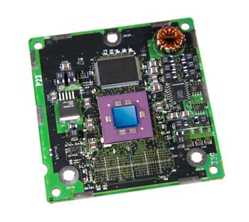
Cache memory is a very high speed semiconductor memory which can speed up the CPU. It acts as a buffer between the CPU and the main memory. It is used to hold those parts of data and program which are most frequently used by the CPU. The parts of data and programs are transferred from the disk to cache memory by the operating system, from where the CPU can access them.
Advantages
The advantages of cache memory are as follows −
- Cache memory is faster than main memory.
- It consumes less access time as compared to main memory.
- It stores the program that can be executed within a short period of time.
- It stores data for temporary use.
Disadvantages
The disadvantages of cache memory are as follows −
- Cache memory has limited capacity.
- It is very expensive.
Primary Memory (Main Memory)
Primary memory holds only those data and instructions on which the computer is currently working. It has a limited capacity and data is lost when power is switched off. It is generally made up of semiconductor device. These memories are not as fast as registers. The data and instruction required to be processed resides in the main memory. It is divided into two subcategories RAM and ROM.
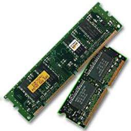
Characteristics of Main Memory
- These are semiconductor memories.
- It is known as the main memory.
- Usually volatile memory.
- Data is lost in case power is switched off.
- It is the working memory of the computer.
- Faster than secondary memories.
- A computer cannot run without the primary memory.
Secondary Memory
This type of memory is also known as external memory or non-volatile. It is slower than the main memory. These are used for storing data/information permanently. CPU directly does not access these memories, instead they are accessed via input-output routines. The contents of secondary memories are first transferred to the main memory, and then the CPU can access it. For example, disk, CD-ROM, DVD, etc.
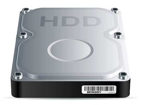
Characteristics of Secondary Memory
- These are magnetic and optical memories.
- It is known as the backup memory.
- It is a non-volatile memory.
- Data is permanently stored even if power is switched off.
- It is used for storage of data in a computer.
- Computer may run without the secondary memory.
- Slower than primary memories.
6. What is Input and Output?
Simply put, inputs and outputs are the ways that a computer (or another device) interacts with the world.
Inputs refer to any way that the computer receives data from outside world. The most obvious examples are your computer’s keyboard, trackpad, or mouse, but “inputs” can also include cameras, microphones, and other devices or systems that supply data to a given computer.
Outputs operate similarly, but in reverse. Outputs enable computers to address the physical world; these devices include displays and speakers, but also controls and signals for tasks like turning lights off and on, controlling motors, and more.
7. How Computer Input and Output Works?
Generally, I/O devices communicate with a computer through an interface called a bus. This interface has two main functions.
1. Interpreting. The bus addresses and performs “handshaking” between the devices using basic commands (like “READY” or “BUSY”). This handshaking allows the devices to communicate with each other successfully.
2. Converting. The interface’s second function is to convert data from serial to parallel or vice versa when necessary. This conversion is what allows devices with different types of information to communicate.
Computers and most other digital systems operate in binary, so any input signal must be in binary by the time it arrives at the computer’s processor. Therefore, any analog inputs go through a conversion to digital using an analog-to-digital converter (ADC) – though that is often part of the device/peripheral itself, as in the case of a scanner. The digital signal that results may also need conversion, as mentioned above, since digital data can be either serial or parallel. At this stage, the bus can typically facilitate conversion between types of digital data.
Conversely, an output bus will facilitate the conversion of the computer’s data into whatever form is needed, whether it’s audio, video, or something else. In some cases, such as with audio, digital information will convert back into analog. Users will need to employ a digital-to-analog converter (DAC) to allow the data to be used with real-world devices.
8. What are the types of I/O?
Types of I/O
There are three types of I/O operations:
Sensory input
- Digital input
- Analog input
Control output
- Direct digital output
- Modulated digital output
- Analog output
Data transfer
- Parallel
- Serial
Notes:
I/O is one of the three main components of a computer system. The responsibility of I/O is to interface with external devices. Depending on their applications, I/O operations can be divided into three groups: sensory input, control output, and data transfer. Once the nature of each type of I/O operation is understood, the hardware design and software for these operations can be understood easily.
Like memory components, I/O components have addresses and each I/O address usually consists of 8 or 16 bits of data. Since many sensory input and control output signals consist of just one bit of information, a single I/O address may be able to handle multiple input and output signals. For instance, some bits of an 8-bit port can be used to receive input signals while other bits are used to send output signals. Depending on how they are used, one bit of an I/O address may be referred to as an I/O port or the set of all bits at a single I/O address may be referred to as an I/O port. When someone says how many ports are needed, you need to find out what his or her definition of port is.
9. Explain The System Bus
An external bus is a communication path between the major components of a computer system such as the CPU and the PM. A bus within the CPU is called an internal bus. Many systems have multiple external buses. Here we limit our discussion to a single external bus, which we call the system bus (or just the bus), that connects the CPU to all the other components of a simple computer system.

The bus is not directly connected to the CPU, the PM, the secondary storage units, and the IO devices. Instead it is connected to each of these unit's controller. The DMA is not a device, but a special kind of control unit that participates in transfers to and from secondary storage units such as the disk and the CD. A bus transaction consists of a two-way communication between two components, during which the bus is normally unavailable for any other communication. The component that initiates a bus transaction is called the initiator, the bus master, or just the master. The master issues a request, such as a read or write, to some other component, which is called the responder or the slave. Common master-slave pairs are BIU-PMC, BIU-IOC, and DMA-PMC. A transaction begins when the master issues a request and ends when the requested action has finished. A particular bus always uses same set of rules for communication between the master and the slave. This set of rules is called the bus protocol and every device attached to the bus must follow these rules. SCSI (small computer system interface), PCI (peripheral component interconnect), and EISA (extended ISA; ISA was the original IBM AT bus) are common protocols found in PCs.
The bus consists of three types of wires, called lines. The control lines, which are collectively called the control bus, transmit the kind of bus transaction (e.g., READ, WRITE) and other information from the master to the slave. In addition the control bus transmits return signals from the slave to the master (e.g., MRC). The address lines, collectively called the address bus, transmit the address of the location within the slave of the data that is to be read (read transaction) or the location into which the data is to be written (write transaction). The data lines, which are collectively called the data bus, transmit the data that is being read or written. Note that even though each of these three sets of lines is called a bus, all of these lines are actually part of the same single bus (the system bus).
A bus has a clock and one period of that clock constitutes a bus cycle, or a bus clock (BCLK) as opposed to a processor (CPU) clock (PCLK). A BCLK is much longer than PCLK. High performance PCs may have a 100 MHz, or slightly higher, bus coupled with a 700 MHz to 1 GHz processor. Normally, the minimum time to transfer a request from the master to a slave or to transfer a response from the slave to the master is one BCLK.
10. What is a DMA Controller explain in detail?
The term DMA stands for direct memory access. The hardware device used for direct memory access is called the DMA controller. DMA controller is a control unit, part of I/O device’s interface circuit, which can transfer blocks of data between I/O devices and main memory with minimal intervention from the processor.
DMA Controller Diagram in Computer Architecture
DMA controller provides an interface between the bus and the input-output devices. Although it transfers data without intervention of processor, it is controlled by the processor. The processor initiates the DMA controller by sending the starting address, Number of words in the data block and direction of transfer of data .i.e. from I/O devices to the memory or from main memory to I/O devices. More than one external device can be connected to the DMA controller.
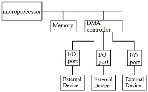
DMA in Computer Architecture
DMA controller contains an address unit, for generating addresses and selecting I/O device for transfer. It also contains the control unit and data count for keeping counts of the number of blocks transferred and indicating the direction of transfer of data. When the transfer is completed, DMA informs the processor by raising an interrupt. The typical block diagram of the DMA controller is shown in the figure below.
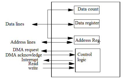
Typical Block Diagram of DMA Controller
Working of DMA Controller
DMA controller has to share the bus with the processor to make the data transfer. The device that holds the bus at a given time is called bus master. When a transfer from I/O device to the memory or vice versa has to be made, the processor stops the execution of the current program, increments the program counter, moves data over stack then sends a DMA select signal to DMA controller over the address bus.
If the DMA controller is free, it requests the control of bus from the processor by raising the bus request signal. Processor grants the bus to the controller by raising the bus grant signal, now DMA controller is the bus master. The processor initiates the DMA controller by sending the memory addresses, number of blocks of data to be transferred and direction of data transfer. After assigning the data transfer task to the DMA controller, instead of waiting ideally till completion of data transfer, the processor resumes the execution of the program after retrieving instructions from the stack.
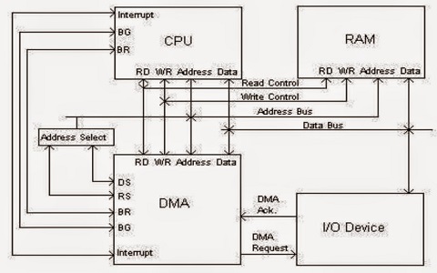
Transfer Of Data in Computer By DMA Controller
DMA controller now has the full control of buses and can interact directly with memory and I/O devices independent of CPU. It makes the data transfer according to the control instructions received by the processor. After completion of data transfer, it disables the bus request signal and CPU disables the bus grant signal thereby moving control of buses to the CPU.
When an I/O device wants to initiate the transfer then it sends a DMA request signal to the DMA controller, for which the controller acknowledges if it is free. Then the controller requests the processor for the bus, raising the bus request signal. After receiving the bus grant signal it transfers the data from the device. For n channeled DMA controller n number of external devices can be connected.
The DMA transfers the data in three modes which include the following.
a) Burst Mode: In this mode DMA handover the buses to CPU only after completion of whole data transfer. Meanwhile, if the CPU requires the bus it has to stay ideal and wait for data transfer.
b) Cycle Stealing Mode: In this mode, DMA gives control of buses to CPU after transfer of every byte. It continuously issues a request for bus control, makes the transfer of one byte and returns the bus. By this CPU doesn’t have to wait for a long time if it needs a bus for higher priority task.
c) Transparent Mode: Here, DMA transfers data only when CPU is executing the instruction which does not require the use of buses.
8237 DMA Controller
- 8237 has 4 I/O channels along with the flexibility of increasing the number of channels.
- Each channel can be programmed individually and has a 64k address and data capability.
- The timing control block, Program command control block, Priority Encoder Block are the three main blocks of 8237A.
- The internal timing and external control signals are driven by the timing control block.
- Various commands given by the microprocessor to the DMA are decoded by program command control block.
- Which channel has to be given the highest priority is decided by the priority encoder block.
8237A has 27 internal registers.
8237A operates in two cycles- Ideal cycle and active cycle, where each cycle contains 7 separate states composed of one clock period each.
S0- The first state, where the controller has requested for the bus and waiting for the acknowledgment from the processor.
S1, S2, S3, S4 are called the working states of the 8237A where the actual transfer of data takes place. If more time is needed for transfer wait states SW are added between these states.
For memory –to- memory transfer read-from-memory and write-to-memory transfers have to be made. Eight states are required for single transfer. The first four states with subscripts S11, S12, S13, S14 does the read-from-memory transfer and the next four S21, S22, S23, S24 are for write-to-memory transfer.
DMA goes into the ideal state when no channel is requesting service and perform SI state. SI is an inactive state where the DMA is inactive until it receives a request. In this state, DMA is in program condition where the processor can program the DMA.
When DMA is in the ideal state and gets no further channel requests, it outputs an HRQ signal to the processor and enters into Active state where it can start the transfer of data either by burst mode, cycle stealing mode or transparent mode.
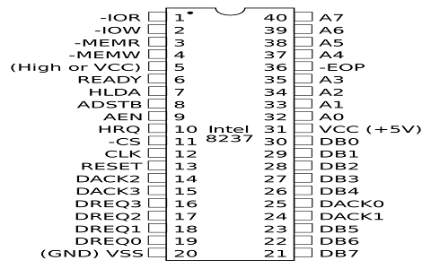
8237 Pin Diagram
8257 DMA Controller
When paired with single Intel 8212 I/O port device, the 8257 DMA controller forms a complete 4 channel DMA controller. Upon receiving a transfer request the 8257 controller-
- Acquires the control over system bus from the processor.
- The peripheral connected to the highest priority channel is acknowledged.
- The least significant bits of the memory address are moved over the address lines A0-A7 of the system bus.
- The most significant 8 bits of the memory address are driven to 8212 I/O port through data lines.
- Generates the appropriate controls signals for the transfer of data between peripherals and addressed memory locations.
- When the specified number of bytes are transferred, the controller informs the CPU end of transfer by activating the terminal count ( TC) output.
For each channel 8257 contains two 16-bit registers– 1) DMA address register and 2) Terminal count register, which should be initialized before a channel is enabled. The address of first memory location to be accessed is loaded in the DMA address register. The lower order 14 bits of the value loaded in the terminal count register indicates the number of DMA cycles minus one before the activation of Terminal count output. Type of operation for a channel is indicated by the most significant two bits of the Terminal count register.
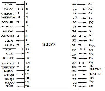
8257 Pin Diagram
Advantages and Disadvantages of DMA Controller
The advantages and disadvantages of DMA controller include the following.
Advantages
- DMA speedups the memory operations by bypassing the involvement of the CPU.
- The work overload on the CPU decreases.
- For each transfer, only a few numbers of clock cycles are required
Disadvantages
- Cache coherence problem can be seen when DMA is used for data transfer.
- Increases the price of the system.
DMA (Direct Memory Access) controller is being used in graphics cards, network cards, sound cards etc… DMA is also used for intra-chip transfer in multi-core processors. Operating in one of its three modes, DMA can considerably reduce the load of the processor