Processor Architecture
Unit 5PIC Interfacing – III Q 1) Explain the basic features of ADC.A 1)Features of ADCThe PIC18f458 has a 10-bit 8 channel A/D converter. The number of analog inputs varies among difference PIC18 devices. Relative accuracy: ±0.19% error maximum Full scale current match: ±1 LSB typ Fast settling time: 150 ns typ Noninverting digital inputs are TTL and CMOS compatible High speed multiplying input slew rate: 8 mA/µs Power supply voltage range: ±4.5V to ±18V Low power consumption: 33 mW @ ±5V The A/D converter has the following registers: A/D Result High Register (ADRESH) A/D Result Low Register (ADRESL) A/D Control Register 0 (ADCON0) A/D Control Register 1 (ADCON1) ADRESH and ADRESL registers hold the result of the A/D conversion and gives 16 bit output.ADCON0 is Control Register used for setting conversion time as well as used to select the input channels.ADCON1 is Control Register used for setting Vref voltage. Q 2) Explain interfacing of ADC and DAC 0808 with PIC.A 2)Interfacing of ADC and DAC 0808 with PICDAC(digital to analog converter) 0808 with Interfacing with PIC The digital-to-analog converter (DAC) is a device widely used to convert digital pulses to analog signals. The DAC0808 is an 8-bit monolithic digital-to-analog converter (DAC). featuring a full scale output current settling time of 150 ns while dissipating only 33 mW with ±5V supplies. No reference current (IREF) trimming is required for most applications since the full scale output current is typically ±1 LSB of 255 IREF/256. Relative accuracies of better than ±0.19% assure 8-bit monotonicity and linearity while zero level output current of less than 4 µA provides 8-bit zero accuracy for IREF≥2 mA. The power supply currents of the DAC0808 are independent of bit codes, and exhibits essentially constant device characteristics over the entire supply voltage range. The DAC0808 IC is a monolithic digital to analog converter which takes an 8-bit digital data as an input and sends an analog signal at the output. It has high accuracy and utilizes very low power. Electronic devices like music players, televisions, mobiles, CD players gaming systems, etc. use this chip for the conversion of audio signals. This article discusses in detail the working, Pinout configuration, Proteus simulation and uses of IC DAC0808. ADC In electronics, an analog-to-digital converter (ADC, A/D, or A-to-D) is a system that converts an analog signal, such as a sound picked up by a microphone or light entering a digital camera, into a digital signal. An ADC may also provide an isolated measurement such as an electronic device that converts an input analog voltage or current to a digital number representing the magnitude of the voltage or current. Typically, the digital output is a two's complement binary number that is proportional to the input, but there are other possibilities. There are several ADC architectures. Due to the complexity and the need for precisely matched components, all but the most specialized ADCs are implemented as integrated circuits (ICs). These typically take the form of metal–oxide–semiconductor (MOS) mixed-signal integrated circuit chips that integrate both analog and digital circuits. Q 3) Write a temperature sensor interfacing using ADC and 12c with pic.A 3) Temperature sensor interfacing using ADC and 12C with PICOBJECTIVE:Temperature measurement Digital display of temperature used of microcontroller to measure temperature used of microcontroller to Display temperature value on LCD (liquid crystal display) The PIC microcontroller measure temperature using LM35 which is an analog temperature sensor every 10 second and compares it with the reference value enters by the user. When the reference value is higher than the measured value, then the heater is turned ON to heat the area. The PIC microcontroller measure temperature using LM35 which is an analog temperature sensor every 10 second and compares it with the reference value enters by the user. When the reference value is higher than the measured value, then the heater is turned ON to heat the area. The heater is switched OFF once the reference temperature is reached. When the measured value is higher than the reference value, then the cooler is switched ON to cool off the area until the required temperature is reached. An LCD display shows the measured temperature continuously. Q 4) Explain interfacing of RTC using 12 with PIC.A 4)Interfacing of RTC using 12 with PICRead date & time by using I2C – RTC in PIC16F/18F Advanced Development Board. Wiring up an I2C based RTC to the I2C port is relatively simple. The RTC also makes the software easier as it takes care of all calendar functions; accounting for leap years etc. The DS1307 (RTC) Real Time Clock IC (an I2C real time clock) is an 8-pin device using an I2C interface. In PIC16F/18F Advanced Development Kit, 2 nos. of RTC lines are controlled by I2C Enabled drivers. I2C Lines serial clock of CLK (RC3), serial data of DATA (RC4) connected to the I2C based serial RTC ds1307 IC. The date & times are read in PIC16F/18F Advanced Development Kit by using these DATA & CLK I2C lines. Q 5) Write a short note on interfacing of EEPROM using SPI with pic.A 5)Interfacing of EEPROM using SPI with PICSPI:Serial Peripheral Interface (SPI) is a synchronous serial data protocol used by microcontrollers for communicating with one or more peripheral devices quickly over short distances. It can also be used for communication between two microcontrollers. Typically, there are three lines common to all the devices Fig. 1 shows how to interface the SPI-DAC to microcontroller. With an SPI connection there is always one master device (usually a microcontroller) which controls the peripheral devices. Typically, there are three lines common to all the devices. Master in Slave Out (MISO) – The Slave line for sending data to the master. Master Out Slave In (MOSI) – The Master line for sending data to the peripherals. Serial Clock (SCK) – The clock pulses which synchronize data transmission generated by the master. Slave Select pin – the pin on each device that the master can use to enable and disable specific devices. When a device’s Slave Select pin is low, it communicates with the master. When it’s high, it ignores the master. These allow you to have multiple SPI devices sharing the same MISO, MOSI, and CLK lines. Q 6) Explain DAC (digital to analog converter) 0808 with Interfacing with PIC 18A 6)The digital-to-analog converter (DAC) is a device widely used to convert digital pulses to analog signals. The DAC0808 is an 8-bit monolithic digital-to-analog converter (DAC). featuring a full scale output current settling time of 150 ns while dissipating only 33 mW with ±5V supplies. No reference current (IREF) trimming is required for most applications since the full scale output current is typically ±1 LSB of 255 IREF/256. Relative accuracies of better than ±0.19% assure 8-bit monotonicity and linearity while zero level output current of less than 4 µA provides 8-bit zero accuracy for IREF≥2 mA. The power supply currents of the DAC0808 is independent of bit codes, and exhibits essentially constant device characteristics over the entire supply voltage range. Features Relative accuracy: ±0.19% error maximum Full scale current match: ±1 LSB typ Fast settling time: 150 ns typ Noninverting digital inputs are TTL and CMOS compatible High speed multiplying input slew rate: 8 mA/µs Power supply voltage range: ±4.5V to ±18V Low power consumption: 33 mW @ ±5V 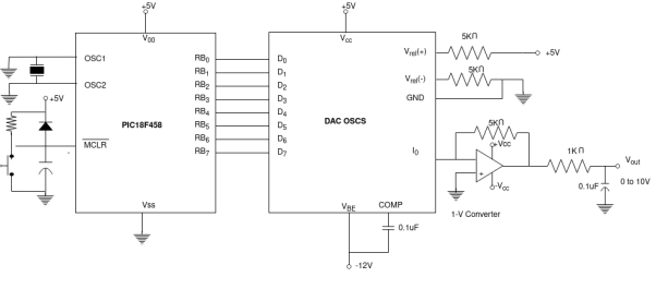 Fig 1. Interfacing of DAC with PIC Q 7) Explain Temperature sensor LM35.A 7)Temperature sensor LM 35
The LM35 is an integrated circuit sensor that can be used to measure temperature with an electrical output proportional to the temperature (in oC). The LM35 device has an advantage over linear temperature sensors calibrated in Kelvin, as the user is not required to subtract a large constant voltage from the output to obtain convenient Centigrade scaling. The LM35 device does not require any external calibration or trimming to provide typical accuracies of ±¼°C at room temperature and ±¾°C over a full −55°C to 150°C temperature range. The low-output impedance, linear output, and precise inherent calibration of the LM35 device makes interfacing to readout or control circuitry especially easy. The device is used with single power supplies, or with plus and minus supplies. As the LM35 device draws only 60 μA from the supply, it has very low selfheating of less than 0.1°C in still air. The LM35 device is rated to operate over a −55°C to 150°C temperature range,while the LM35C device is rated for a −40°C to 110°C range (−10° with improved accuracy). The LM35-series devices are available packaged in hermetic TO transistor packages, while the LM35C, LM35CA, and LM35D devices are available in the plastic TO-92 transistor package. The LM35D device is available in an 8-lead surface-mount small-outline package and a plastic TO-220 package. In LM35 circuit, parameter values commonly used are: Vc = 4 to 30v 5v or 12 v are typical values used. Ra = Vc /10-6 Actually, it can range from 80 KW to 600 KW , but most just use 80KW. Interfacing of LM 35 with PIC 18f458 Here LM 35 is connected to the PORT A0 and LCD is connected to the PORT B. The LM35 measure temperature with an electrical output proportional to the temperature (in oC). LM35 temperature sensor converts temperature into its proportional analog voltage value. LM35 is three terminal device.Pin number one and three are for 5-volt voltage supply. Pin two is analog voltage output with respect to temperature value.Relation between measured temperature and analog output voltage is 1oC = 10m volt. Hence for every 1 degree increase in temperature there will be a increment of 10m volt in output voltage of LM35 sensor. PIC18F microcontroller is used to measure analog voltage value. PIC18F microcontroller built in ADC (analog to digital converter) is used to measure analog voltage. PIC18F PORTA have seven built in ADC channels. After reading ADC value, using voltage and temperature relationship voltage is converted back into temperature. A conversion factor is used to convert voltage back into temperature. All these conversion has been done through programming. LCD is connected to PORTB of PIC18 microcontroller to display output.
Q 8) Draw interfacing diagram of PIC 18 with ADC.A 8) 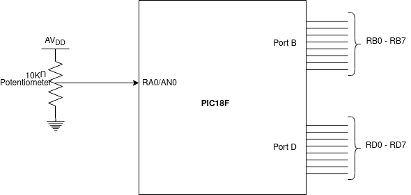 Fig. Interfacing of PIC18 with ADC
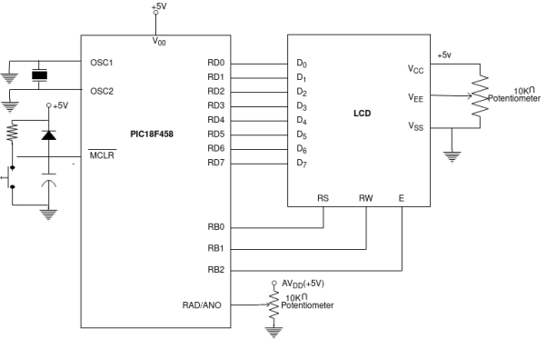 Fig. Interfacing PIC18F458 with analog voltageQ 9) Explain ADCON1 register.
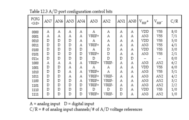
ADCON1 is 8 bit register. ADCON1 is Control Register used for setting Vref voltage. Bit 7 ADFM: A/D result format select bit Bit 6 ADCS2: A/D conversion clock select. This bit along with the ADCS1:ADCS0 bits of ADCON0 are used to select clock source for A/D conversion. 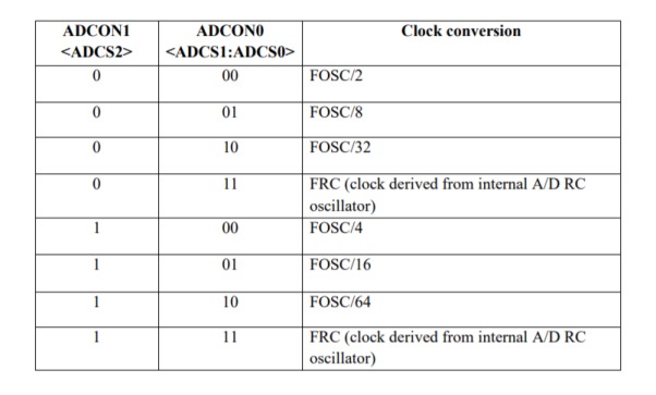 Bit 3-0 PCFG3:PCFG0: A/D port configuration control bits
 Q 10) Explain ADS.A 10)
In electronics, an analog-to-digital converter (ADC, A/D, or A-to-D) is a system that converts an analog signal, such as a sound picked up by a microphone or light entering a digital camera, into a digital signal. An ADC may also provide an isolated measurement such as an electronic device that converts an input analog voltage or current to a digital number representing the magnitude of the voltage or current. Typically, the digital output is a two's complement binary number that is proportional to the input, but there are other possibilities. There are several ADC architectures. Due to the complexity and the need for precisely matched components, all but the most specialized ADCs are implemented as integrated circuits (ICs). These typically take the form of metal–oxide–semiconductor (MOS) mixed-signal integrated circuit chips that integrate both analog and digital circuits.
 Fig 1. Interfacing of DAC with PIC Q 7) Explain Temperature sensor LM35.A 7)Temperature sensor LM 35
 Fig. Interfacing of PIC18 with ADC
 Fig. Interfacing PIC18F458 with analog voltageQ 9) Explain ADCON1 register.
- 0 = left justified. Six least significant bits of ADRESL are 0s.
- 1 = right justified. Most significant bits of ADRESH are 0s.
 Bit 3-0 PCFG3:PCFG0: A/D port configuration control bits
 Q 10) Explain ADS.A 10)
0 matching results found