UNIT 5
UNIT 5
Semiconductor Diodes
- Write a short note on semi-conductors.
A semiconductor is a substance whose resistivity lies between the conductors and insulators. The property of resistivity is not the only one that decides a material as a semiconductor, but it has few properties as follows.
- Semiconductors have the resistivity which is less than insulators and more than conductors.
- Semiconductors have negative temperature co-efficient. The resistance in semiconductors, increases with the decrease in temperature and vice versa.
- The Conducting properties of a Semiconductor changes, when a suitable metallic impurity is added to it, which is a very important property.
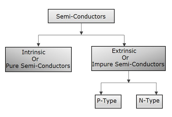
Semiconductor devices are extensively used in the field of electronics. The transistor has replaced the bulky vacuum tubes, from which the size and cost of the devices got decreased and this revolution has kept on increasing its pace leading to the new inventions like integrated electronics. The following illustration shows the classification of semiconductors.
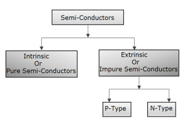
2. Explain Intrinsic and extrinsic Semiconductors.
A Semiconductor in its extremely pure form is said to be an intrinsic semiconductor. The properties of this pure semiconductor are as follows −
- The electrons and holes are solely created by thermal excitation.
- The number of free electrons is equal to the number of holes.
- The conduction capability is small at room temperature.
In order to increase the conduction capability of intrinsic semiconductor, it is better to add some impurities. This process of adding impurities is called as Doping. Now, this doped intrinsic semiconductor is called as an Extrinsic Semiconductor.
Doping
The process of adding impurities to the semiconductor materials is termed as doping. The impurities added, are generally pentavalent and trivalent impurities.
Pentavalent Impurities
- The pentavalent impurities are the ones which has five valence electrons in the outer most orbit. Example: Bismuth, Antimony, Arsenic, Phosphorus
- The pentavalent atom is called as a donor atom because it donates one electron to the conduction band of pure semiconductor atom.
Trivalent Impurities
- The trivalent impurities are the ones which has three valence electrons in the outer most orbit. Example: Gallium, Indium, Aluminum, Boron
- The trivalent atom is called as an acceptor atom because it accepts one electron from the semiconductor atom.
Extrinsic Semiconductor
An impure semiconductor, which is formed by doping a pure semiconductor is called as an extrinsic semiconductor. There are two types of extrinsic semiconductors depending upon the type of impurity added. They are N-type extrinsic semiconductor and P-Type extrinsic semiconductor.
N-Type Extrinsic Semiconductor
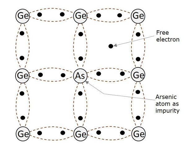
A small amount of pentavalent impurity is added to a pure semiconductor to result in Ntype extrinsic semiconductor. The added impurity has 5 valence electrons.
For example, if Arsenic atom is added to the germanium atom, four of the valence electrons get attached with the Ge atoms while one electron remains as a free electron. This is as shown in the following figure.
All of these free electrons constitute electron current. Hence, the impurity when added to pure semiconductor, provides electrons for conduction.
- In N-type extrinsic semiconductor, as the conduction takes place through electrons, the electrons are majority carriers and the holes are minority carriers.
- As there is no addition of positive or negative charges, the electrons are electrically neutral.
- When an electric field is applied to an N-type semiconductor, to which a pentavalent impurity is added, the free electrons travel towards positive electrode. This is called as negative or N-type conductivity.
P-Type Extrinsic Semiconductor
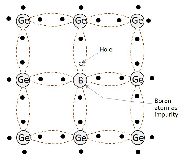
A small amount of trivalent impurity is added to a pure semiconductor to result in P-type extrinsic semiconductor. The added impurity has 3 valence electrons. For example, if Boron atom is added to the germanium atom, three of the valence electrons get attached with the Ge atoms, to form three covalent bonds. But, one more electron in germanium remains without forming any bond. As there is no electron in boron remaining to form a covalent bond, the space is treated as a hole. This is as shown in the following figure.
The boron impurity when added in a small amount, provides a number of holes which helps in the conduction. All of these holes constitute hole current.
- In P-type extrinsic semiconductor, as the conduction takes place through holes, the holes are majority carriers while the electrons are minority carriers.
- The impurity added here provides holes which are called as acceptors, because they accept electrons from the germanium atoms.
- As the number of mobile holes remains equal to the number of acceptors, the Ptype semiconductor remains electrically neutral.
- When an electric field is applied to a P-type semiconductor, to which a trivalent impurity is added, the holes travel towards negative electrode, but with a slow pace than electrons. This is called as P-type conductivity.
- In this P-type conductivity, the valence electrons move from one covalent bond to another, unlike N-type.
3.Why Silicon is Preferred in Semiconductors?
Among the semiconductor materials like germanium and silicon, the extensively used material for manufacturing various electronic components is Silicon Si. Silicon is preferred over germanium for many reasons such as −
- The energy band gap is 0.7ev, whereas it is 0.2ev for germanium.
- The thermal pair generation is smaller.
- The formation of SiO2 layer is easy for silicon, which helps in the manufacture of many components along with integration technology.
- Si is easily found in nature than Ge.
- Noise is less in components made up of Si than in Ge.
Hence, Silicon is used in the manufacture of many electronic components, which are used to make different circuits for various purposes. These components have individual properties and particular uses.
4. Give a detailed explanation of P-N JUNCTION.
When a semi-conductor is doped such that half the portion is doped with the trivalent impurity (Al, Ar, Bi) and the other half is doped with pentavalent impurity (B, P) then the junction formed is known as PN junction.
Its symbol is
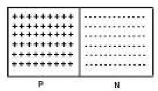
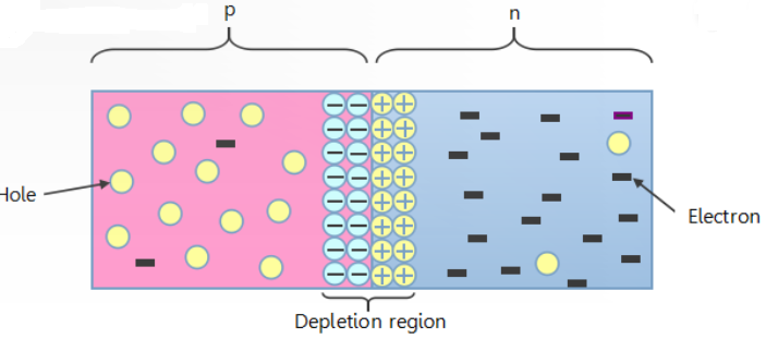
Depletion layer
At normal condition, the holes from P region diffuse into N region and electrons from N region diffuse in P region.
A thin layer of positive ion is formed in the N region and negative ions in the P region near the junction are formed.
This thin layer that is formed is known as depletion layer.

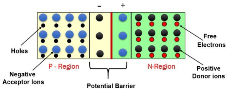
Barrier potential
The potential barrier in the PN-junction diode is the barrier in which the charge requires additional force for crossing the depletion region.
Here, the depletion region acts as a barrier and opposes the flow of charge carrier.
Depending on the type of material used, the value of barrier potential lies between 0.3 – 0.7V.
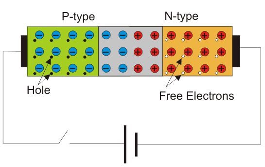
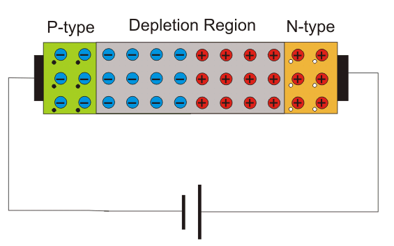
Forward Biased P-N Junction
When p-type region is connected with the positive terminal and n-type region with the negative terminal of the voltage source, then the junction is said to be forward biased.
At this condition, due to the attraction of cathode, electrons create covalent bond in p-type material and are attracted towards the terminal.
Hence, numbers of covalent bonds are broken and electrons moves towards the positive terminal increasing the concentration of electrons in the crystal nearer to the terminal and these electrons recombine with holes here.
In this way, the number of holes increases in the p-type region away from the junction, and it is reduced in the portion of p-type region nearer to the terminal.
Due to the higher concentration of holes adjacent to negative impurity ions layer the electrons of negative ions come out and recombine with those holes and create new holes in the layer.
Consequently, the width of this negative ions layer is reduced and finally this layer vanishes.
Reverse Biased PN Junction
When positive terminal is connected to the n-type region and the negative terminal is connected to the p-type region then the pn junction is said to be in reverse biased condition.
When no voltage applied across the p n junction, the potential developed across the junction is 0.3 volts at 25oC for germanium and 0.7 volts at 25oC for silicon p n junction.
The polarity of this potential barrier is same as the polarity of voltage source applied during reverse biased condition.
Now if reverse biased voltage is increased the barrier potential developed also increases. Hence, the pn junction widens.
The free electrons of the n-type region are attracted towards positive terminal of the source because of that more positive impurity ions are created in the depletion layer which makes the layer thicker.
At the same time, electrons are injected in the p-type region. Due to the positive potential of the n-type region the electrons are drifted towards the junction and combine with holes and create more positive impurity ions in the layer.
4. Write and explain various Break down voltages.
In the reverse bias, the voltage increases in the reverse direction but no current across the p-n junction due to the majority carriers. Only a very small leakage current flow. But at a certain reverse voltage p-n junction breaks in conduction. It is only due to the minority carriers. This amount of voltage is sufficient for these minority carriers to break the depletion region. At this moment sharp current flows through the junction. This breakdown of voltage is of two types.
- Avalanche Breakdown: It is not sharp, rather it is an inclined linear graph i.e. after break down small increase in reverse voltage causes sharper current.
- Zener Breakdown: It is sharp and there is no need to increase reverse bias voltage to get more current, because current already flows sharply.
5. Draw and explain PIV characteristics of PN junction diode.
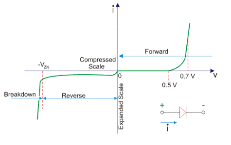
In the forward bias, the operational region is in the first quadrant.
The threshold voltage for Germanium is 0.3 V and for Silicon is 0.7 V.
Beyond this, the graph goes upward in a non-linear manner.
This graph is for the dynamic Resistance of the junction in the forward bias.
6. Explain Half and full wave rectifier.
A complete half-wave rectifier circuit consists of 3 main parts:
- A transformer
- A resistive load
- A diode
A half wave rectifier circuit diagram looks like this:
First, a high AC voltage is applied to the to the primary side of the step- down transformer and we will get a low voltage at the secondary winding which will be applied to the diode.
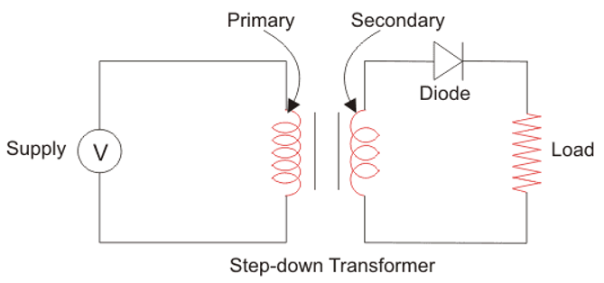
During the positive half cycle of the AC voltage, the diode will be forward biased and the current flows through the diode. During the negative half cycle of the AC voltage, the diode will be reverse biased and the flow of current will be blocked. The final output voltage waveform on the secondary side (DC) is shown in figure above.
If we replace the secondary transformer coils with a source voltage, we can simplify the circuit diagram of the half-wave rectifier as:

For the positive half cycle of the AC source voltage, the equivalent circuit effectively becomes:
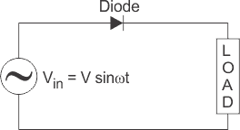
This is because the diode is forward biased, and is hence allowing current to pass through. So, we have a closed circuit.
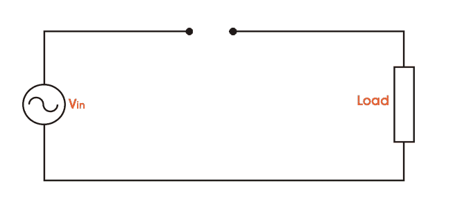
But for the negative half cycle of the AC source voltage, the equivalent circuit becomes:
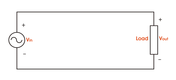
Because the diode is now in reverse bias mode, no current is able to pass through it. As such, we now have an open circuit. Since current cannot flow through to the load during this time, the output voltage is equal to zero.
This all happens very quickly – since an AC waveform will oscillate between positive and negative many times each second (depending on the frequency).
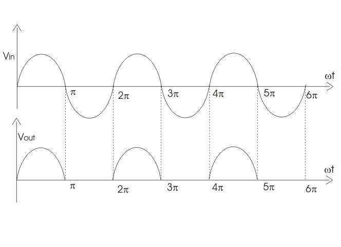
Here’s what the half wave rectifier waveform looks like on the input side (Vin), and what it looks like on the output side (Vout) after rectification (i.e. conversion from AC to DC):
The graph above actually shows a positive half wave rectifier. This is a half-wave rectifier which only allows the positive half-cycles through the diode,and blocks the negative half-cycle.
The voltage waveform before and after a positive half wave rectifier is shown in figure 4 below.
Conversely, a negative half-wave rectifier will only allow negative half-cycles through the diode and will block the positive half-cycle. The only difference between a posive and negative half wave rectifier is the direction of the diode.
As you can see in figure 5 below, the diode is now in the opposite direction. Hence the diode will now be forward biased only when the AC waveform is in its negative half cycle.

ADVANTAGES:-
1)Simple Construction.
2) Component required less.
3)Small size.
APPLICATION:-
Walkman, low-cost power supply.
TRANSFORMER UTILISATION FACTOR(TUF): It indicates how well the ilp transformer is being utilized
TUF= DC O/P Power / AC power rating of the transformer

Full wave rectifier
1) A center-tapped rectifier is a type of full-wave rectifier that uses two diodes connected to the secondary of a center-tapped transformer.
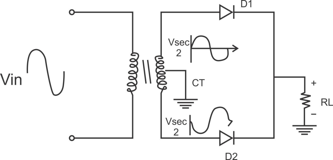
Center tapped full wave rectifier operation:-
I) During the positive half cycle of the i/p ac supply.
Diagram

D1.Is in forward biased & D2 is in reverse biased.
II)During -ve half cycle.

D1 Reverse biased
D2 Forward biased
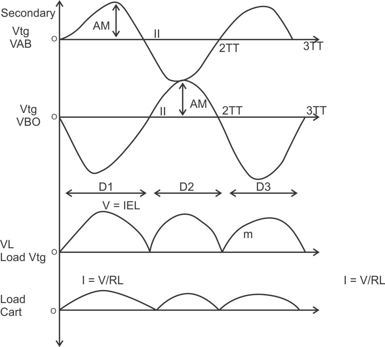
ADVANTAGES
- Law ripple factor as Compared to HKR.
- Better rectification efficiency.
- Better TUF.
- A higher value of average load vtg&avg load crt.
- No possibility of transformer core saturation.
DISADVANTAGES
PIV of the diode is 2vm, more size costly.
APPLICATION
I) Battery charges.
2)power supply at the laboratory, high current, electronic ckt.
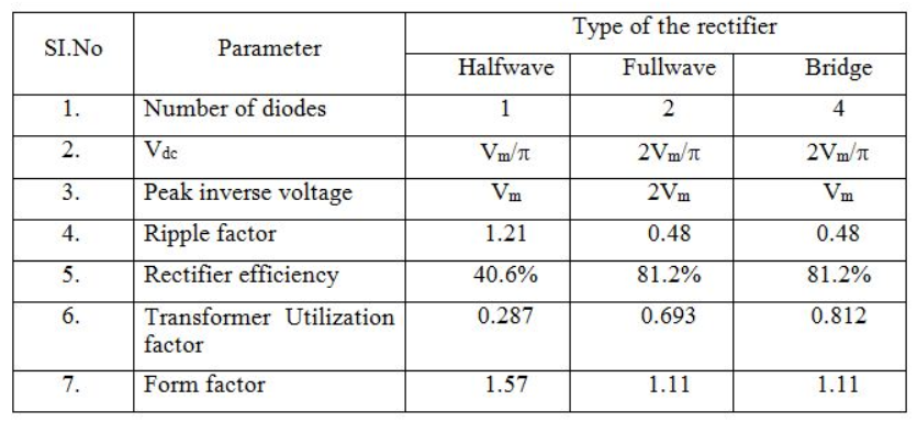
7. What is Zener and avalanche Breakdown? Explain.
The Zener Breakdown is observed in the Zener diodes having Vz less than 5V or between 5 to 8 volts. When a reverse voltage is applied to a Zener diode, it causes a very intense electric field to appear across a narrow depletion region. Such an intense electric field is strong enough to pull some of the valence electrons into the conduction band by breaking their covalent bonds. These electrons then become free electrons which are available for conduction. A large number of such free electrons will constitute a large reverse current through the Zener diode and breakdown is said to have occurred due to the Zener effect.
Characteristics of Zener Breakdown is shown below:
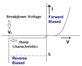
Zener Breakdown Characteristics
A current limiting resistance should be connected in series with the Zener diode to protect it against the damage due to excessive heating. In Zener breakdown, the breakdown voltage depends on the temperature of P-N junction. The breakdown voltage decreases with increase in the junction temperature.
Avalanche Breakdown
The avalanche breakdown is observed in the Zener Diodes having Vz having than 8 V. In the reverse biased condition, the conduction will take place only due to the minority carriers. As we increase the reverse voltage applied to the Zener diode, these minority carriers tend to accelerated. Therefore, the kinetic energy associated with them increases. While travelling, these accelerated minority carriers will collide with the stationary atoms and impart some of the kinetic energy to the valence electrons present in the covalent bonds.
Characteristics of Avalanche Breakdown is shown below:
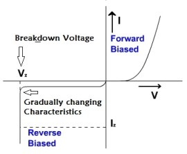
Avalanche Breakdown Characteristics
Due to this additionally acquired energy, these valence electrons will break their covalent bonds and jump into the conduction bond to become free conduction. Now these newly generated free electrons will get accelerated. They will knock out some more valence electrons by means of collision. This phenomenon is called as carrier multiplication.
8. Draw and explain Zener Diode – Operation, characteristics, and Application.
- Zener diode is a special type of p-n junction semiconductor diode in this diode the reverse breakdown voltage is adjusted precisely between 3v to 200v.
- Its applications are based on this principle hence Zener diode is called as a breakdown diode.
- The doping level of the imparity added to manufacture the zener diode is controlled in order to adjust the precise value of breakdown voltage.
PRINCIPLE OF OPERATION:-A zener diode can be forward biased or reverses biased. Its operation in the forward biased mode is same as that of a p-n junction diode but its operation in the reverse biased mode is sustainably deferent.

CHARACTERISTICS:
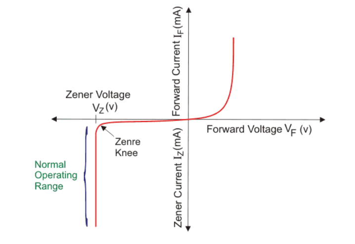
- A graph of current through vs the voltage across the device is called the characteristic of Zener diode.
- The first quadrant is the forward biased region. Here the Zener diode acts like an ordinary diode.
- When a forward voltage is applied, current flows through it. But due to higher doping concentration, higher current flows through the Zener diode
- In the third quadrant, the magic happens. The graph shows the current vs voltage curve when we apply a reverse bias to the diode.
- The Zener breakdown voltage is the reverse bias voltage after which a significant amount of current starts flowing through the Zener diode.
- Here in the diagram, VZ refers to the Zener breakdown voltage. Until the voltage reaches Zener breakdown level, tiny amount of current flows through the diode. Once the reverse bias voltage becomes more than the Zener breakdown voltage, a significant amount of current starts flowing through the diode due to Zener breakdown.
- The voltage remains at the Zener breakdown voltage value, but the current through the diode increases when the input voltage gets increased. Due to the unique property of Zener diode, the depletion region regains its original position when the reverse voltage gets removed.
- The Zener diode doesn’t get damaged despite this massive amount of current flowing through it.
APPLICATIONS:
Zener diodes are used for voltage regulation, as reference elements, surge suppressors, and in switching applications and clipper circuits.
9. Draw and explain PHOTODIODE.
The photodiode is a p-n junction semiconductor diode which is always operated in the reverse biased condition.
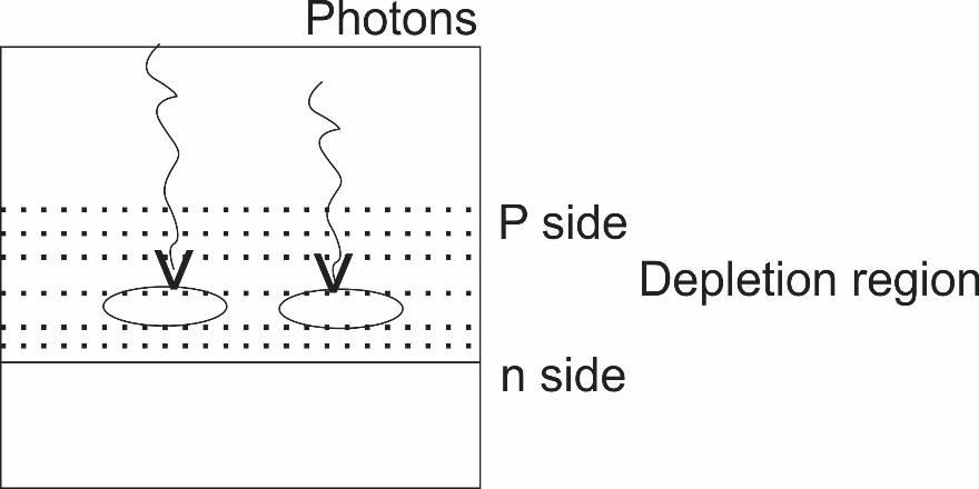
The light is always focused through a glass lens on the junction of the photodiode As the photodiode is reverse biased the depletion region is quite wide, penetrated on both sides of the junction.
The photons incident on the depletion region will impact their energy to the Ions present in the depletion region and generates e hole pairs.
The photons incident on the depletion region, so the number of electron hole pairs will be generated, depends on the intensity of light [number of photons] These and holes will be attracted towards the +ve& -ve terminals respectively of the photocurrent.
With an increase in the light intensity more number of e hole pairs are generated and the photocurrent increases thus the photocurrent is proportional to the light intensity.
10. Draw and explain LED.
An LED emits light when electrical energy is applied to it. For proper operation, it is necessary to forward bias the LED.
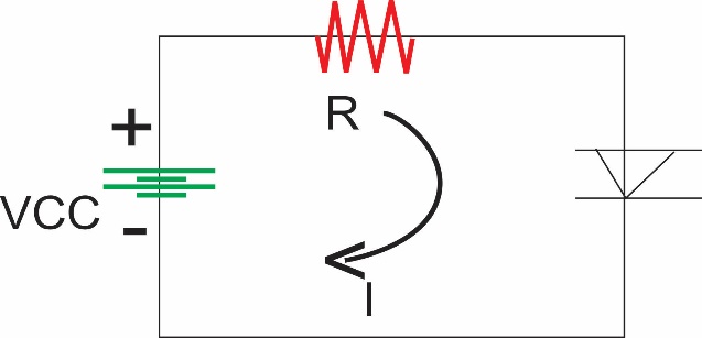
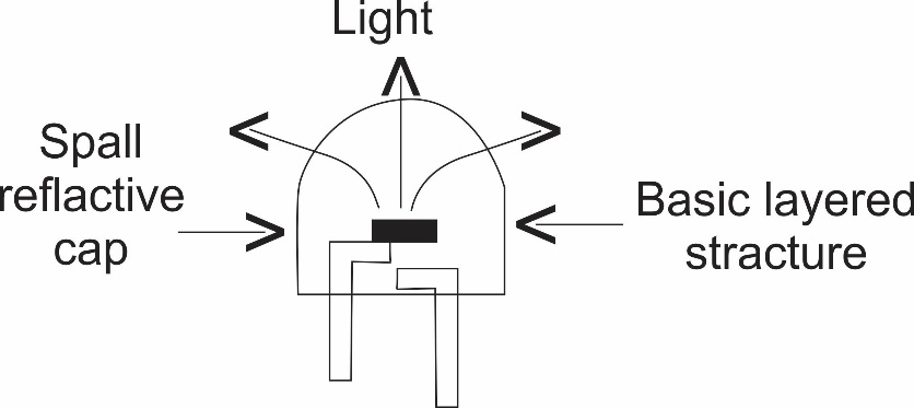
Construction of LED:-
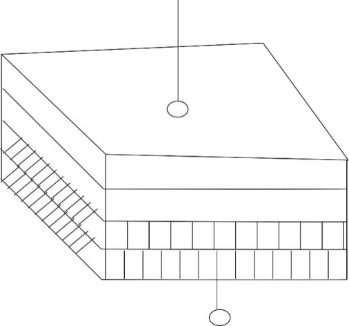
To make the emission of light in one direction cup type construction is used for LED.
PRINCIPLE LED OPERATION
When the led is forward biased the electrons in the n-region will cross the junction and recombine with the holes in the p-type material.
These free e- reside in the conduction band & hence at a higher energy level than the holes in the valence band
When recombination takes place this e- return peak to the valence band which is at a lower energy level than the conduction band.
While returning back the recombining e-give away the excess energy in the form of light. This process is called electroluminescence. In this way an LED emits light.
Color of the Emitted Light
Material Use Color of Emitted Light
i) Gallium Arsenide (GOAS) In fared (IR)
Ii) GaASP(gallium arsenide Red or Yellow
phosphide)
Iii) Gallium phosphide (GAP) Red or Green
Application
Used in 7 Segment Display