UNIT-1
SEMICONDUCTOR PHYSICS
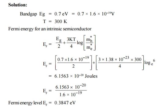
Q 1) For an intrinsic Semiconductor with a band gap of 0.7 eV, determine the position of EF at T = 300 K if m*h = 6m*e
A1)
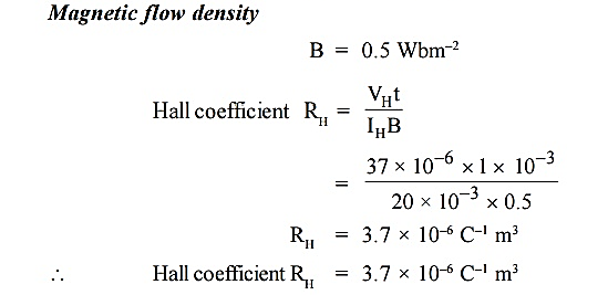
Q 2) A semiconducting crystal with 12 mm long, 5 mm wide and 1 mm thick has a magnetic density of 0.5 Wbm–2 applied from front to back perpendicular to largest faces. When a current of 20 mA flows length wise through the specimen, the voltage measured across its width is found to be 37μV . What is the Hall coefficient of this semiconductor?
A 2)

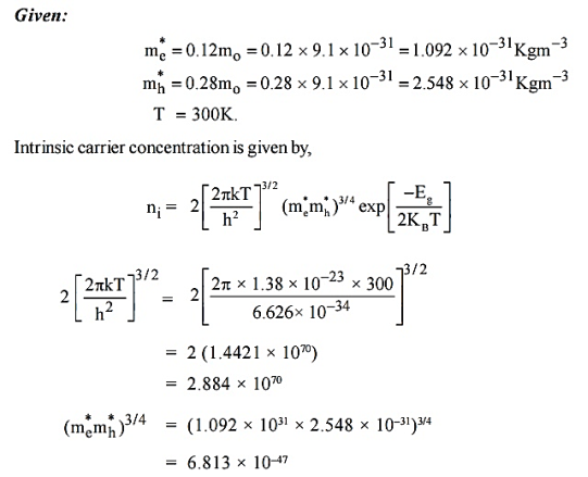
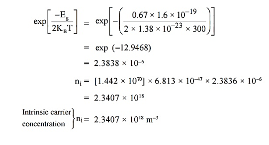
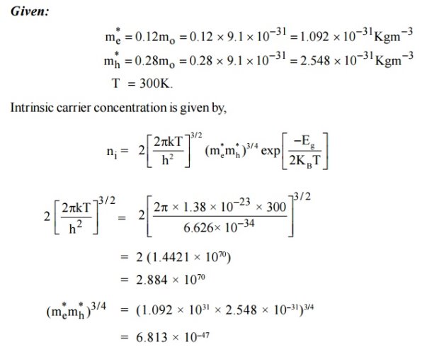
Q 3) Calculate the intrinsic concentration of charge carriers at 300 K given that m *e =0.12m o ,m *h =0.28mo and the value of brand gap = 0.67 eV.
A 3)
Q 4) Explain the term Fermi level and Fermi energy?
A 4)
Fermi level" is the term used to describe the top of the collection of electron energy levels at absolute zero temperature. This concept comes from Fermi-Dirac statistics. Electrons are fermions and by the Pauli Exclusion Principle cannot exist in identical energy states. So at absolute zero they pack into the lowest available energy states and build up a "Fermi sea" of electron energy states. The Fermi level is the surface of that sea at absolute zero where no electrons will have enough energy to rise above the surface.
The concept of the Fermi energy is a crucially important concept for the understanding of the electrical and thermal properties of solids. Both ordinary electrical and thermal processes involve energies of a small fraction of an electron volt. But the Fermi energies of metals are on the order of electron volts. This implies that the vast majority of the electrons cannot receive energy from those processes because there are no available energy states for them to go to within a fraction of an electron volt of their present energy. Limited to a tiny depth of energy, these interactions are limited to "ripples on the Fermi sea".
At higher temperatures a certain fraction, characterized by the Fermi function, will exist above the Fermi level. The Fermi level plays an important role in the band theory of solids. In doped semiconductors, p-type and n-type, the Fermi level is shifted by the impurities, illustrated by their band gaps. The Fermi level is referred to as the electron chemical potential in other contexts.
In metals, the Fermi energy gives us information about the velocities of the electrons which participate in ordinary electrical conduction. The amount of energy which can be given to an electron in such conduction processes is on the order of micro-electron volts (see copper wire example), so only those electrons very close to the Fermi energy can participate. The Fermi velocity of these conduction electrons can be calculated from the Fermi energy.
This speed is a part of the microscopic Ohm's Law for electrical conduction. For a metal, the density of conduction electrons can be implied from the Fermi energy. | 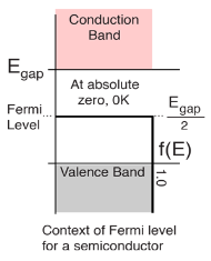 Figure 4: Fermi level for a Semiconductor
|
The Fermi energy also plays an important role in understanding the mystery of why electrons do not contribute significantly to the specific heat of solids at ordinary temperatures, while they are dominant contributors to thermal conductivity and electrical conductivity. Since only a tiny fraction of the electrons in a metal are within the thermal energy kT of the Fermi energy, they are "frozen out" of the heat capacity by the Pauli principle. At very low temperatures, the electron specific heat becomes significant.
It is named after the Physicist Enrico Fermi. A Fermi level is the measure of the energy of least tightly held electrons within a solid. It is important in determining the thermal and electrical properties of solids. It can be defined as:
The Fermi energy is a concept in quantum mechanics usually refers to the energy difference between the highest and lowest occupied single-particle states in a quantum system of non-interacting fermions at absolute zero temperature.
The value of the Fermi level at absolute zero temperature is known as the Fermi energy. It is also the maximum kinetic energy an electron can attain at 0K. Fermi energy is constant for each solid.
To determine the lowest possible Fermi energy of a system, we first group the states with equal energy into sets and arrange them in increasing order of energy. We then add particles one at a time, successively filling up the unoccupied quantum states with the lowest energy.
When all the particles are arranged accordingly, the energy of the highest occupied state is the Fermi energy.
In Spite of the extraction of all possible energy from metal by cooling it to near absolute zero temperature (0 Kelvin), the electrons in the metal still move around. The fastest ones move at a velocity corresponding to a kinetic energy equal to the Fermi energy.
The highest energy level that an electron can occupy at the absolute zero temperature is known as the Fermi Level. The Fermi level lies between the valence band and conduction band because at absolute zero temperature the electrons are all in the lowest energy state. Due to lack of sufficient energy at 0 Kelvin, the Fermi level can be considered as the sea of fermions (or electrons) above which no electrons exist. The Fermi level changes as the solids are warmed and as electrons are added to or withdrawn from the solid.
Don’t get confuse between Fermi level and Fermi energy. Both the terms are equal at absolute zero temperature but they are different at other temperature.
Q 5) Define Fermi function also discuss effect of temperature on Fermi function
A 5)
Fermi function F (E):
Fermi-Dirac distribution function represents the probability of an electron occupying a given energy level at absolute temperature. It is given by

Where KB Boltzmann Constant
T Temperature
If g(E) is the density of states and f(E) gives the probability of occupation of those states at a given temperature, the number of occupied states, n(E),is given by
n(E) =  (1)
(1)
If the number of occupied states in an energy band needs to be calculated the integration needs to be performed over the entire band. This will be a function of temperature, since the Fermi function is temperature dependent. Equation 1 can be used to calculate the concentration of electron and holes in semiconductors, which decides their conductivity.
Effect of temperature on Fermi Function:
Case (i) Probability of occupation for E < EF at T = 0K

When T = 0K and E < EF, we have
F(E) =  =
=  = 1
= 1
Thus at T = 0K, there is 100 % chance for the electrons to occupy the energy levels below the Fermi level.
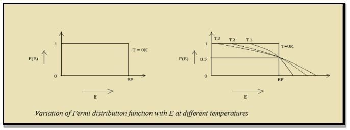
Figure 3: Fermi distribution
Case (ii) Probability of occupation for E>EF at T = 0K
When T = 0K and E > EF, we have
F(E) =  =
=  =
=  = 0
= 0
Thus, there is 0 % chance for the electrons to occupy energy levels above the Fermi energy level. From the above two cases, at T = 0K the variation of F(E) for different energy values becomes a step function.
Case (iii) Probability of occupation at ordinary temperature
At ordinary temperature, the value of probability starts reducing from 1 for values of E slightly less than EF. With the increase of temperature, i.e., T> 0K, Fermi function F (E) varies with E.
At any temperature other than 0K and E = EF
F(E) =  =
=  =
=  = 50%
= 50%
Hence, there is 50 % chance for the electrons to occupy Fermi level. Further, for E > EF the probability value falls off rapidly to zero.
Case (iv) At high temperature
When kT >> EF, the electrons lose their quantum mechanical character and Fermi distribution function reduces to classical Boltzmann distribution
Q 6) Explain Fermi level for intrinsic semiconductors and what is the effect of temperature on Fermi level?
A 6)
Fermi Level
We know that in intrinsic semiconductor
Electron concentration ‘n’ = Hole concentration ‘p’
Equating Equations (15) and (27), we get
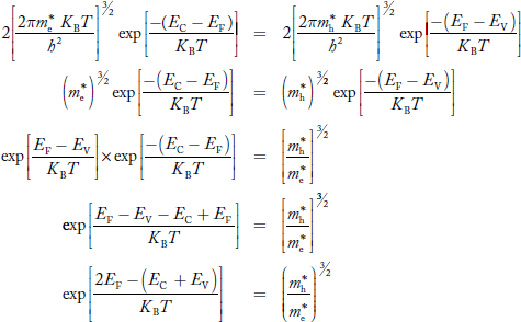
Taking logarithms on both sides, we get
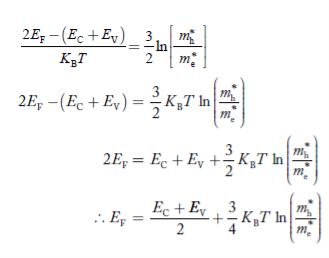 ……………… (29)
Normally, mh* is greater than me*, since ln  is very small so that EF is just lie in the middle of energy gap
Temperature effect on Fermi level
Fermi level slightly rises with increase of temperature.
But in case of pure intrinsic semiconductor like Si and Ge,
mh* ≈ me*
So in these cases Fermi level lies at the middle of energy gap.
Q 7) Derive expression for carrier concentration for intrinsic semiconductors?
A 7)
Intrinsic semiconductors—carrier concentration
Here we will calculate the number of electrons excited into conduction band at temperature T and also the hole concentration in the valence band. It is assumed that the electrons in the conduction band behave as if they are free particles with effective mass me* and the holes near the top of the valence band behave as if they are free particles with effective mass mh*.
Here we will calculate the electron concentration, hole concentration
Density of Electrons in Conduction Band
The number of free electrons per unit volume of semiconductor having energies in between E and E + dE is represented as N(E) dE
dE = width of Energy band
Therefore, we have:
N(E) dE = ge(E) dE fe(E) ……….(1)
ge(E) = The density of electron states per unit volume
fe(E) = Fermi-Dirac distribution function i.e. probability that an electron occupies an electron state
The number of electrons present in the conduction band per unit volume of material ‘n’ is obtained by integrating N(E) dE between the limits Ec and Ect
Where Ec = the bottom energy levels of conduction band
Ect = the bottom and top energy levels of conduction band
n =  ……….(2)
Can be written as
n =  =
= 
n =  -
-  ……….(3)
We know that above Ect, there is no electrons.
Hence, Equation (3) becomes
n =  -
- 
n =  ……….(4)
The Fermi-Dirac distribution function fe(E) can be represented as:
 (E) =
(E) = ……….(5)
Compared to the exponential value, so the ‘1’ in the denominator can be neglected.
So  >>1
>>1
Hence,  (E) =
(E) = =
=  ……….(6)
The density of electron states ge(E) in the energy space from E = 0 to E can be written as:
 (E) =
(E) =  [
[ ]3/2 (E - 0) ½ ……….(7)
Where me* is the effective mass of an electron and h is Planck’s constant.
 (E)dE =
  [
[ ]3/2 (E - 0) ½dE ……….(8)
To evaluate n, the density of states is counted from Ec, since the minimum energy state in conduction band is Ec. So eq (8) can become
 (E)dE =
  [
[ ]3/2 (E - Ec) ½dE ……….(9)
Substituting Equations (6) and (9) in (4) gives
n =  3/2
3/2 (E-
(E- )1/2
)1/2 dE
dE
n = [
[ ]3/2
]3/2  1/2
1/2 dE ………… (10)
The above equation can be simplified by the following substitution:
Put ɛ = E − Ec ………… (11)
So, dɛ = dE
In Equation (11), Ec is constant, as we change the variable E to ε in Equation (10), the integral limits also change.
In Equation (11), as E → Ec then ε → 0 and E → ∞, then ε also → ∞.
The exponential term in Equation (10) becomes:
 = exp [
 ] = exp [
 ]
]

 ………… (12)
Substituting Equations (11) and (12) in (10), we get:
n = [
[ ]3/2
]3/2  dE
dE
n = [
[ ]3/2
]3/2
 dE ………… (13)
Above integral (I) can be simplified by substitution. Put ε = x2
So that dɛ = 2x dx
I = 2x dx
2x dx
= dx
dx
= =
= T)3/2 ………… (14)
Substituting Equation (14) in (13) gives:
n = [
[ ]3/2
]3/2 T)3/2
T)3/2
n =
n = 
n =  ………… (15)
The term  is almost a constant compared with the exponential term as the temperature changes. So, it is a pseudo constant and is given by the symbol Nc. So, we have
n =Nc ………… (16)
Density of Holes in Valence Band
The number of holes per unit volume of semiconductor in the energy range E and E + dE in valence band is represented as P(E) dE. Proceeding same way( as in case of electrons) we have
Therefore, we have:
P(E) dE = gh(E) dE fh(E) ……….(17)
dE = width of Energy band
gh(E) = The density of holes states per unit volume
fh(E) = Fermi-Dirac distribution function i.e. probability that an hole occupies an electron state
The number of electrons present in the conduction band per unit volume of material ‘n’ is obtained by integrating P(E) dE between the limits Evb and EV
Where EV = the bottom energy levels of valence band
Evb = the bottom and top energy levels of valence band
The total number of holes present in the valence band per unit volume of material ‘p’ is obtained by integrating P(E) dE
 ……….(18)
Equation (18) can be represented as:
 ……….(19)
Now we know that below Evb no holes is present. Hence, Equation (19) becomes
 ……….(20)
We know hole can also be defined as absence of an electron.
Presence of a hole = the absence of an electron
Hence, the Fermi-Dirac function of holes fh(E) in the valence band is:
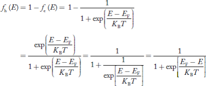
Compared to exponential, the ‘1’ in the denominator is negligible,

Hence,
 ……….(21)
The density of hole states between E and E + dE in valence band can be written similar to Equation (8.9) for electrons.
 ……….(22)
Where mh* is the effective mass of hole.
Substituting Equations (21) and (22) in (20),
 ……….(23)
The above equation can be simplified by the substitution:
Put ɛ = EV − E ............. (24)
So dɛ = − dE
In Equation (24), EV is constant, as we change the variable E to ε in Equation (23), the integral limits also change.
In Equation (24),
As E → EV then ε → 0
And E→ −∞, then ε → ∞
The exponential term in Equation (23) becomes:
 ............. (25)
Substituting Equations (24) and (25) in (23), we get:
 ………….(26)
From Equation (14), we know the integral value  T)3/2 put here and we get
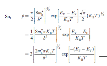 ………….(27)
….The term  is almost constant compared with the exponential term as the temperature changes. So, it is a pseudo constant and is given by the symbol NV. So, we have
 …………… (28)
Q 8) Where Fermi level lie in case of p type and n type extrinsic semiconductor?
Or
Derive expression for Carrier Concentration in Extrinsic Semiconductors.
A 8)
Carrier Concentration in Extrinsic Semiconductors
The number of charge carriers present per unit volume of a semiconductor material is called carrier concentration.
Suppose donor and acceptor atoms are doped in a semiconductor.
At temperature T K,
n = number of conduction electrons
p = number of holes
N−A = number of acceptor ions
N+D = number of donor ions
We know that the below equation hold good in semiconductor. The total negative charge due to conduction electrons and acceptor ions is equal to holes and donor ions in unit volume of material.
So the material will be considered neutral if,
n + N−A = p + N+D ……….(34)
Equation (34) is called charge neutrality equation.
In the above equation
 ………..(35)
Concentration of acceptor ions N−A = acceptor concentration x probability of finding an electron in acceptor level
 ………..(36)
Similarly, the donor ions concentration is

 ………..(37)
In n-type material
Note
nn represents electrons in n-type material
pn represents holes concentration in n-type material.
There are no acceptor atoms so N−A = 0.
At 0 K, all the electron states in donor level are occupied by electrons.
As the temperature is increased from 0 K, some of the electrons jump from these donor states into the conduction band.
Also the concentration of holes is extremely less compared with the concentration of conduction electrons [p << n]
From Equation (34) we have
n = p N+D
(Or) n ≈ N+D …………(38) [since p << N+D]
At temperature T K,
As the temperature increase Almost all the donor atoms donate electrons to conduction band.

So, in n-type material, the free electron concentration is almost equal to the donor atoms.
So we can rewrite the above equation as
nn ≈ ND …………….(39)
Where nn represents electrons in n-type material
Also the hole concentration in n-type material can be obtained by applying law of mass action nn pn =ni2
 …………..(40)
Where pn represents holes concentration in n-type material.
In n-type material at 0 K, the Fermi energy level lies in the middle of Ec and ED

At temperature> 0K
 ……….(41)
With increase in temperature the Fermi level shifts upwards according to Equation (61) slightly due to ionization of donor atoms.
With further increase of temperature, electron-hole pairs are generated due to the breaking of covalent bonds, hence Fermi level shifts downwards.
In p-type semiconductor
Note
pp represents holes in p-type material
np represents electrons in p-type material
There are no donor atoms so means no ions present  = 0.
= 0.
At 0 K, all the acceptor levels are not occupied by electrons.
As the temperature is increased from 0 K, some electrons jump from top valence band energy levels to the acceptor states, leaving holes in the valence band and acceptor ions  are formed.
At some room temperature T K, concentration of conduction electrons is extremely less compared with hole concentration.
∴ From Equation (34), we have
n + N−A = p ……………(42)
(or) N−A ≈ p ……………. (43) [since n << N−A]
At temperature T K, in p-type material,
The hole concentration is almost equal to the acceptor atoms in unit volume of the material.
So, Equation (43) can be written as
pp ≈ NA ……………….(44)
Where pp represents holes in p-type material
The electron concentration in p-type material can be obtained by applying law of mass action as nppp = ni2
 …………….(45)
Where np represent free electron concentration in p-type material.
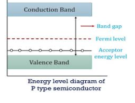
In p-type material, the Fermi level lies in between EV and EA at 0 K

As the temperature is increased from 0 K, the Fermi level shifts downwards slightly as per Equation (46) due to ionization of acceptor atoms.
And with further increase of temperature, electron-hole pairs are generated due to the breaking of covalent bonds, so Fermi level shifts upwards.
Q 9) Derive hall coefficient? Show how hall coefficient and mobility are related?
A 9)
When the magnetic field is applied perpendicular to a current-carrying conductor, then a voltage is developed in the material perpendicular to both the magnetic field and current in the conductor. This effect is known as Hall Effect and the voltage developed is known as Hall voltage (VH).
Hall Effect is useful to identify the nature of charge carriers in material and hence to decide whether the material is an n-type semiconductor or p-type semiconductor, also to calculate carrier concentration and mobility of carriers.
Hall Effect can be explained by considering a rectangular block of an extrinsic semiconductor in which current is flowing along the positive X-direction and magnetic field B is applied along Z-direction as shown in Figure.

11 Figure: Hall Effect
Suppose if the semiconductor is n-type, then mostly the carriers are electrons and the electric current is due to the drifting of electrons along negative X-direction or if the semiconductor is p-type, then mostly the carriers are holes and the electric current is due to drifting of the holes along positive X-direction.
As these carriers are moving in the magnetic field in the semiconductor that means they experience Lorentz force represented by FL
FL = Bevd
Where vd is the drift velocity of the carriers. (already explained in the previous section).
We can obtain the direction of this force by applying Fleming’s left-hand rule in electromagnetism.
Fleming’s left-hand rule can be explained as If we stretch the thumb, forefinger, and middle finger in three perpendicular directions so that the forefinger is parallel to the magnetic field and the middle finger is parallel to the current direction, then the thumb represents the direction of the force on the current-carrying carriers.
So the Lorentz force is exerted on the carriers in the negative Y-direction. Due to Lorentz force, more and more carriers will be deposited at the bottom face (represented by face 1in the figure) of the conductor.
The deposition of carriers at the bottom face is continued till the repulsive force due to accumulated charge balances the Lorentz force.
After some time of the applied voltage, both the forces become equal in magnitude and act in opposite direction, then the potential difference between the top and bottom faces is equal to Hall voltage and that can be measured.
At equilibrium, the Lorentz force on a carrier
FL = Bevd ……………..(1)
And the Hall force
FH = eEH ……………..(2)
Where EH is the Hall electric field due to accumulated charge.
At equilibrium, FH = FL
EEH = Bevd
∴ EH = Bvd ……………..(3)
If ‘d’ is the distance between the upper and lower surfaces of the slab, then the Hall field
EH =  ……………..(4)
In n-type material, Jx = –nevd
vd = -  ……………..(5)
Where n is free electron concentration, substituting (5) in (3), we have
∴ EH = -B  ……………..(6)
For a given semiconductor, the Hall field EH is proportional to the current density Jx and the intensity of magnetic field ‘B’ in the material.
i.e. EH ∝ JxB
(or) EH = RHJxB ……………..(7)
Where RH = Hall coefficient
Equations (6) and (7) are the same so, we have
RHJxB =-B 
RH = -  = -
= -  ……………..(8)
Where ρ is the charge density
Similarly for p-type material
RH =  =
= ……………..(9)
Using Equations (8) and (9), carrier concentration can be determined.
Thus, the Hall coefficient is negative for n-type material. In n-type material, as the more negative charge is deposited at the bottom surface, so the top face acquires positive polarity and the Hall field is along negative Y-direction. The polarity at the top and bottom faces can be measured by applying probes.
Similarly, in the case of p-type material, a more positive charge is deposited at the bottom surface. So, the top face acquires negative polarity and the Hall field is along positive Y-direction. Thus, the sign of the Hall coefficient decides the nature of (n-type or p-type) material.
The Hall coefficient can be determined experimentally in the following way:
Multiplying Equation (7) with ‘d’, we have
EHd = VH = RHJxBd ……………..(10)
From (Figure 15) we know the current density Jx
Jx = 
Where W is the width of the box. Then, Equation (10) becomes
VH = RH Bd = RH
RH =  ……………..(11)
Substituting the measured values of VH, Ix, B, and W in Equation(11), RH is obtained. The polarity of VH will be the opposite for n- and p-type semiconductors.
The mobility of charge carriers can be found by using the Hall effect, for example, the conductivity of electrons is
n = neμn
Or we can rewrite it as
μn =  =n RH ……………..(12)
By using equation (11)
μn = n ……………..(13)
Q 10) Discuss the application of the Hall Effect?
A 10)
• Using magnetic flux leakage – To properly inspect items such as pipes or tubes, Hall Effect probes work with something called magnetic flux leakage. This is a way of testing such items, and being able to spot potential corrosion, erosion, or pitting. This is specifically used in steel items and can give important information about lifespan or safety.
• Sensors to detect rotation speed – A Hall Effect probe can be used in bicycle wheels, speedometers in the automotive world, electronic types of ignition systems, and gear teeth.
• Used to detected movement – You will often find a Hall Effect probe used in such items as Go-Kart controls, smartphones, paintball guns, or airsoft guns, as well as some GPS systems.
• Ferrite Toroid Hall Effect current transducers – This is mainly used in electronic compasses, making use of the magnetic field to show direction.
• Split-ring clamp-on sensors – These types of Hall Effect probes are used to test equipment without having to take the whole circuit board apart, e.g. Complex items.
• Analog multiplication – Anything which needs a power measurement, e.g. Sensing, and is also used in small computers.
• General power measurement – Any device which needs to be tested for its power input can be done by a Hall Effect probe.
• Position and motion sensors – This is mainly used in a DC motor, often the brushless type.
• The automotive world – Hall Effect probes are used widely in the automotive world, especially in fuel injection and ignition. Wheel rotation sensors also use Hall Effect probes, e.g. For anti-lock braking.
- For determination of the type of given semiconductor.
- For N-type, Hall coefficient RH= negative
- For P-type, Hall coefficient RH= Positive
- To determine carrier concentration n and p; that is n=p=1/e𝑅𝐻
- Determination of mobility of charge carriers μn =
 =n RH. Where 𝜎= electrical conductivity
 - To determine the sign of charge carriers whether the conductivity is due to electrons or holes.
Main Advantages of Using Hall Sensors
Why is a Hall Effect probe advantageous in all of these instances? Because the probes are not affected by outside influences, e.g. Water or dirt. They can also easily sense the measure of the output they need when they are placed in the right position. On top of this, Hall Effect probes are safer, because the voltage never actually makes it directly to the sensor/probe. This makes this type of measurement overall so much safer than other methods.
As you can see, understanding how something is put into practice in the real world helps you to understand it in real terms. The Hall Effect is certainly very commonplace these days, in much more methods and applications than we realize. While certainly very useful in the automation world, even basic items such as a compass make large use of this scientific approach.
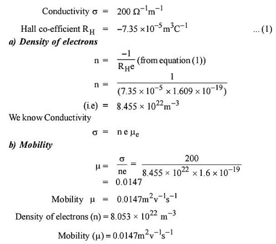
Q 11) The Hall coefficient of certain silicon specimen was found to be –7.35 × 10⁻⁵ m3 C–1 from 100 to 400 K. Determine the nature of the semiconductor. If the conductivity was found to be 200 –1 m–1. Calculate the density and mobility of the charge carrier.
A 11)
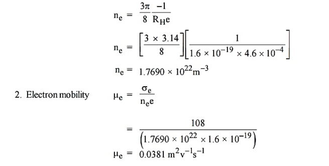
Q 12) An N-type semiconductor has hall coefficient = 4.16 × 10⁻⁴ m3 C–1. The conductivity is 108 m–1. Calculate its charge carrier density ‘ne’and electron mobility at room temperature.
A 12)

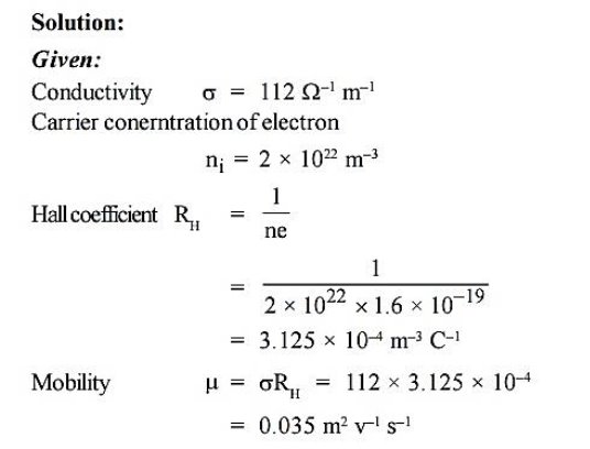
Q 13) In an N-type semiconductor, the concentration of electron is 2 × 10²² m–3. Its electrical conductivity is 112 m–1. Calculate the mobility of electrons.
A 13)
Q 14) Calculate the intrinsic concentration of charge carriers at 300 K given that m *e =0.12m o ,m *h =0.28mo and the value of brand gap = 0.67 eV.
A 14)
