UNIT-8
INTRODUCTION TO QUANTUM MECHANICS AND NANOTECHNOLOGY
Q 1) Discuss Bottom up approach?
A 1)
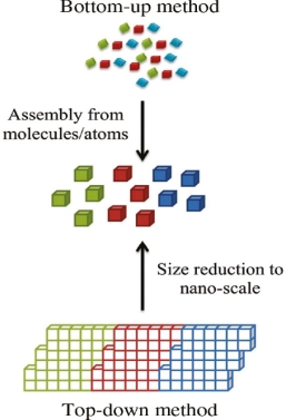
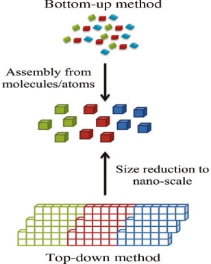
In bottom-up approaches nanomaterials are assembled from basic building blocks, such as molecules or nanoclusters. The basic building blocks, in general, are nanoscale objects with suitable properties that can be grown from elemental precursors. The concept of the bottom-up approach is that the complexity of nanoscale components should reside in their self-assembled internal structure, requiring as little intervention as possible in their fabrication from the macroscopic world.
The bottom-up approach uses atomic or molecular feed-stocks as the source of the material to be chemically transformed into larger nanoparticles. This has the advantage of being potentially much more convenient than the top down approach. By controlling the chemical reactions and the environment of the growing nanoparticle, then the size, shape and composition of the nanoparticles may all be affected. For this reason nanoparticles produced by bottom up, chemically based and designed, reactions are normally seen as being of higher quality and having greater potential applications. This has led to the growth of a host of common bottom up strategies for the synthesis of nanoparticles. Many of these techniques can be tailored to be performed in gas, liquid, solid states, hence the applicability of bottom-up strategies to a wide range of end products. Most of the bottom up strategies requires suitable organometallic complexes or metal salts to be used as chemical precursors, which are decomposed in a controlled manner resulting in particle nucleation and growth. One of the key differences that can be used to subdivide these strategies into different categories is the method by which the precursor is decomposed.
A typical example of bottom-up is processing for nanocomposite magnets from individual high-magnetization and high-coercivity nanoparticles. The assembling critically depends on availability of anisotropic (single crystal) hard magnetic nanoparticles. Anisotropic nanoparticles produced via surfactant-assisted high energy ball milling satisfy the major requirements for this application.
Q 2) Discuss Top down approach?
A 2)
In top-down approaches, a bulk material is restructured (i.e. partially dismantled, machined, processed or deposited) to form nanomaterials. The aggressive scaling of electronic integrated circuits in recent years can be considered the greatest success of this paradigm. For top-down methods, the challenges increase as devices size is reduced and as the desired component designs become larger and more complex. Also the top-down assembly of nanocomponents over large areas is difficult and expensive.
The top-down method involves the systematic breakdown of a bulk material into smaller units using some form of grinding mechanism. This is beneficial and simple to execute and avoids the use of volatile and poisonous compounds frequently found in the bottom-up techniques. However, the quality of the nanoparticles formed by grinding is accepted to be poor in comparison with the material produced by modern bottom up methods. The main drawbacks include defect problems from grinding equipment, low particle surface areas, asymmetrical shape and size distributions and high energy needed to produce relatively small particles. Apart from these disadvantages, it must be distinguished that the nano-material produced from grinding still finds use, due to the simplicity of its manufacture, in applications including magnetic, catalytic and structural properties.
Q 3) Write applications of nanotechnology?
A 3)
APPLICATIONS
Scanning electron microscopy has been applied to the surface studies of metals, ceramics, polymers, composites and biological materials for both topography as well as compositional analysis.
- An extension of this technique is Electron Probe Micro Analysis (EPMA), where the emission of X-rays, from the sample surface, is studied upon exposure to a beam of high energy electrons.
- Depending on the type of detectors used this method is classified in to two as: Energy Dispersive Spectrometry (EDS) and Wavelength Dispersive Spectrometry (WDS). This technique is used extensively in the analysis of metallic and ceramic inclusions, inclusions in polymeric materials and diffusion profiles in electronic components.
Nano materials possess unique and beneficial, physical, chemical and mechanical properties; they can be used for a wide verity of applications.
Material technology
- Nanocrystalline aerogel are light weight and porous, so they are used for insulation in offices homes, etc.
- Cutting tools made of Nano crystalline materials are much harder, much more wear- resistance, and last stranger.
- Nano crystalline material sensors are used for smoke detectors, ice detectors on air craft wings, etc.
- Nano crystalline materials are used for high energy density storage batteries.
- Nano sized titanium dioxide and zinc dioxide is used in sunscreens to absorb and reflect ultraviolet rays.
- Nano coating of highly activated titanium dioxide acts as water repellent and antibacterial.
- The hardness of metals can be predominately enhanced by using nanoparticles.
- Nanoparticles in paints change colour in response to change in temperature or chemical environment, and reduce the infrared absorption and heat loss.
- Nano crystalline ceramics are used in automotive industry as high strength springs, ball bearings and valve lifters.
Information technology
- Nanoscale fabricated magnetic materials are used in data storage
- Nanocomputer chips reduce the size of the computer.
- Nano crystalline starting light emitting phosphors are used for flat panel displays.
- Nanoparticles are used for information storage.
- Nanophotonic crystals are used in chemical optical computers.
Biomedical
- Biosensitive nanomaterials are used for ragging of DNA and DNA chips.
- In the medical field, nanomaterials are used for disease diagnosis, drug delivery and molecular imaging.
- Nano crystalline silicon carbide is used for artificial heart valves due to its low weight and high strength.
Energy storage
- Nanoparticles are used hydrogen storage.
- Nano particles are used in magnetic refrigeration.
- Metal nanoparticles are useful in fabrication of ionic batteries.
- Nano materials possess unique and beneficial, physical, chemical and mechanical properties; they can be used for a wide verity of applications.
Material technology
- Nanocrystalline aerogel are light weight and porous, so they are used for insulation in offices homes, etc.
- Cutting tools made of Nano crystalline materials are much harder, much more wear- resistance, and last stranger.
- Nano crystalline material sensors are used for smoke detectors, ice detectors on air craft wings, etc.
- Nano crystalline materials are used for high energy density storage batteries.
- Nano sized titanium dioxide and zinc dioxide is used in sunscreens to absorb and reflect ultraviolet rays.
- Nano coating of highly activated titanium dioxide acts as water repellent and antibacterial.
- The hardness of metals can be predominately enhanced by using nanoparticles.
- Nanoparticles in paints change colour in response to change in temperature or chemical environment, and reduce the infrared absorption and heat loss.
- Nano crystalline ceramics are used in automotive industry as high strength springs, ball bearings and valve lifters.
Information technology
- Nanoscale fabricated magnetic materials are used in data storage
- Nanocomputer chips reduce the size of the computer.
- Nano crystalline starting light emitting phosphors are used for flat panel displays.
- Nanoparticles are used for information storage.
- Nanophotonic crystals are used in chemical optical computers.
Biomedical
- Biosensitive nanomaterials are used for ragging of DNA and DNA chips.
- In the medical field, nanomaterials are used for disease diagnosis, drug delivery and molecular imaging.
- Nano crystalline silicon carbide is used for artificial heart valves due to its low weight and high strength.
Energy storage
- Nanoparticles are used hydrogen storage.
- Nano particles are used in magnetic refrigeration.
- Metal nanoparticles are useful in fabrication of ionic batteries.
Q 4) Write physical and chemical properties of nanomaterials ?
A 4)
Physical properties
Inter atomic distance: When the material size is reduced to Nano scale, surface area to volume ratio increases. Due to increase of surface of surface area, more number of atoms will appear at the surface of compared to those inside. So Interatomic spacing decreases with size.
Thermal properties: Nano materials are different from that of bulk materials. The Debye Temperature and ferroelectric phase transition temperature are lower for nano materials. The melting point of nano gold decreases from 1200 K to 800K as the size of particle decreases form 300 Å to 200 Å.
Optical properties: Different sized nano particles scatters different of light incident on it and hence they appear with different colours. For example nano gold does not act as bulk gold. The nano particles of gold appear as orange, purple, red or greenish in colour depending on their grain size. The bulk copper is opaque whereas nanoparticle copper is transparent.
Magnetic properties: The magnetic properties of nano materials are different from that of bulk materials. In explaining the magnetic behaviour of nanomaterials, we use single domains unlike large number of domains in bulk materials. The coercivity value of single domain is very large.
For example, Fe, Co, and Ni are ferromagnetic in bulk but they exhibit super par magnetism. Na, K, and Rh are paramagnetic in bulk but they exhibit ferro-magnetic. Cr is anti-ferromagnetic in bulk but they exhibit super paramagnetic.
Mechanical properties: The mechanical properties such as hardness, toughness, elastic modulus, young’s modulus etc., of nano materials are different from that of bulk materials. In metals and alloys, the hardness and toughness are increased by reducing the size of the nano particles. In ceramics, ductility and super plasticity are increased on reducing grain size. Hardness increases 4 to 6 times as one goes from bulk Cu to nanocrystalline and it is 7 to 8 times for Ni.
Chemical properties
Nanocrystalline materials are strong, hard, erosion and corrosion resistant. They are chemically active and have the following chemical properties.
1. In electrochemical reactions, the rate of increase in mass transport increases as the particle size decreases.
2. The equilibrium vapour pressure, chemical potentials and solubilites of nanoparticles are greater than that for the same bulk material.
3. Most of the metals do not absorb hydrogen. But the hydrogen absorption increases with the decrease of cluster size in Ni, Pt and Pd metals.
Q 5) Explain Davisson-Germer experiment ?
A 5)
In this experiment, Davisson and Germer scattered a 54 eV monoenergetic beam of electrons from a nickel (Ni) crystal. The electron source and detector were symmetrically located with respect to the crystal’s normal, as shown in figure this is similar to the Bragg setup for X-ray diffraction by a grating. What Davisson and Germer found was that, although the electrons are scattered in all directions from the crystal, the intensity was a minimum at θ = 35°
WAVE ASPECT OF PARTICLES
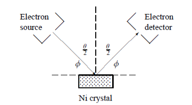
Figure 1: Davisson–Germer experiment: electrons strike the crystal’s surface at an angle ϕ
The detector, symmetrically located from the electron source, measures the number of electrons scattered at an angle θ, where θ is the angle between the incident and scattered electron beams.
It is maximum at θ = 50°; that is, the bulk of the electrons scatter only in well-specified directions. They showed that the pattern continued even when the intensity of the beam was so low that the incident electrons were sent one at a time. This can only result from a constructive interference of the scattered electrons. The reflected electrons formed diffraction patterns that were identical
With Bragg’s X-ray diffraction by a grating instead of the diffuse distribution pattern.
In fact, the intensity maximum of the scattered electrons in the Davisson–Germer experiment corresponds to the first maximum (n = 1) of the Bragg formula,
nλ = 2d sin ϕ
Where d is the spacing between the Bragg planes
ϕ is the angle between the incident ray and the crystal’s reflecting planes
θ is the angle between the incident and scattered beams
d is given in terms of the separation D between successive atomic layers in the crystal by d = D sin θ
For an Ni crystal, we have d = 0.091 nm, since D = 0.215 nm. Since only one maximum is seen at θ = 50° for a mono-energetic beam of electrons of kinetic energy 54 eV, and since 2ϕ +  = π and hence sin ϕ = cos(θ /2) from figure.
We can obtain the wavelength associated with the scattered electrons:
λ =  sin ϕ =
  cos
cos  θ =
θ =  cos 25° = 0.165 nm
Now using results from de Broglie’s relation we will calculate the numerical value of λ. Since the kinetic energy of the electrons is K = 54 eV, and the momentum is p = with mec2 = 0.511 MeV.
Where mec2 is the rest mass energy of the electron and hc  197.33 eV nm, we can show that the de Broglie wavelength is
λ =  =
=
 = 0.167 nm
This is in excellent agreement with the experimental value.
We have seen that the scattered electrons in the Davisson–Germer experiment produced interference fringes that were identical to those of Bragg’s X-ray diffraction. Since the Bragg formula provided an accurate prediction of the electrons’ interference fringes, the motion of an electron of momentum must be described by means of a plane wave
ψ(r, t) =Aei(k·r−ωt) = Aei(p·r−Et)/
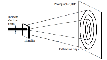
Figure 2: Davisson–Germer experiment
Q 6) How nanomaterial can differentiate from bulk material?
A 6)
When the material size of the object is reduced to nanoscale, then it exhibits different properties than the same material in bulk form. The factors that differentiates the nanomaterials from bulk material is
1. Increase in surface area to volume ratio
2. Quantum confinement effect
Increase in surface area to volume ratio: The ratio of surface area to volume ratio is large for nano materials.
Example 1: To understand this let us consider a spherical material of radius ‘r’. Then its surface area to volume ratio is 3/r. Due to decrease of r, the ratio increases predominantly.
Example 2: For one cubic volume, the surface ratio is 6m2. When it is divided into eight cubes its surface area becomes 12m2. When it is divided into 27 cubes its surface area becomes 18m2. Thus, when the given volume is divided into smaller pieces the surface area increases.

Due to increase of surface of surface area, more number of atoms will appear at the surface of compared to those inside. For example, a nanomaterial of size 10nm has 20% of its atoms on its surface and 3nm has 50% of its atoms. This makes the nanomaterials more chemically reactive and affects the properties of nanomaterials.
Quantum confinement effect: According to band theory, the solid atoms have energy bands and isolated atoms possess discrete energy levels. Nano materials are the intermediate state to solids and atoms. When the material size is reduced to nanoscale, the energy levels of electrons change. This effect is called quantum confinement effect. This affects the optical, electrical and magnetic properties of nanomaterials.
Q 7) Discuss the Classification of Nanomaterials in detail?
A 7)
In the past two decades, hundreds of novel NSMs (nanostructured materials) have been obtained therefore, the need in their classification become important.
NSMs as a subject of nanotechnology are low dimensional materials comprising of building units of a submicron or nanoscale size at least in one direction and exhibiting size effects.
The first classification idea of NSMs was given by Gleiter in 1995 and further was explained by Skorokhod in 2000. However, Gleiter and Skorokhod scheme was not fully considered because of 0D, 1D, 2D, and 3D structures such as fullerenes, nanotubes, and nanoflowers were not taken into account.
After them Pokropivny and Skorokhod reported a modified classification scheme for NSMs, in which 0D, 1D, 2D and 3D NSMs are included.
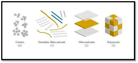
0D Nanostructured Materials
In the past 10 years, significant progress has been made in the field of 0D NSMs. 0D NSMs such as uniform particles arrays (quantum dots), heterogeneous particles arrays, core–shell quantum dots, onions, hollow spheres and nanolenses have been synthesized by several research groups. 0D NSMs, such as quantum dots has been extensively studied in light emitting diodes (LEDs), solar cells, single-electron transistors, and lasers.
A 0D structure is the simplest block that can be used for the design of nanomaterials. In this case, the three dimensions are in the nanometre regime and have a diameter less than 100 nm. Nanoparticles, nanocrystals, and nanoclusters correspond to this group.
Nanoparticles
They are nanostructures usually used to define all 0D nanostructures or those that are amorphous and have an irregular shape. So, the nanoparticles can be of natural origin, semiconductor, metal, oxides, fullerenes or quantum dots.
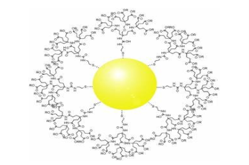
During manufacturing, the nanoparticles that make up the nanomaterials can be of different sizes, which can vary by more than 15% and still form the nanomaterial without affecting its design. 3D nanomaterials should not be included in the category of nanostructures unless their internal structure is nanostructured.
Nanoclusters
As well as the nanoparticles, they have an irregular structure besides being semi crystalline, but they are tinier than the nanoparticles. Its diameter ranges between 1 and 10 nm.
Also nanoclusters are sensitive to their size and become more reactive if they increase or decrease proportionally.
Nanocrystals
They are monocrystalline nanostructures, whose size ranges from 1 to 30 nm. Semiconductor nanocrystals are more commonly known as quantum dots.
One-dimensional nanomaterials (1D)
In the last decade, 1D NSMs have stimulated an increasing interest due to their importance in research and developments and have a wide range of potential applications. It is generally accepted that 1D NSMs are ideal systems for exploring a large number of novel phenomena at the nanoscale and investigating the size and dimensionality dependence of functional properties.
They are also expected to play an important role as both interconnects and the key units in fabricating electronic, optoelectronic, and EEDs with nanoscale dimensions. The field of 1D NSMs such as nanotubes has attained a significant attention. 1D NSMs have a profound impact in nanoelectronics, nanodevices and systems, nanocomposite materials, alternative energy resources and national security. We show the 1D NSMs, such as nanowires, nanorods, nanotubes, nanobelts, nanoribbons, and hierarchical nanostructures, which have been synthesized in the laboratories. They have a variable length, conserving two dimensions (height and width) in the nanometer regime; to these correspond the nanowires and nanotubes.
Nanowires
They are elongated crystalline structures whose characteristics stand out for their conductive or semiconducting properties. Nanowires have been obtained from various metallic materials, semiconductors, oxides, etc. In recent years, nanowires have shown special scientific interest due to their potential applications in nanoelectronics, optoelectronics, and sensors.
Nanotubes
They are tubular structures with a hollow interior. There are nanotubes synthesized and characterized from inorganic laminar materials. However, the most studied are carbon nanotubes (CNT's).
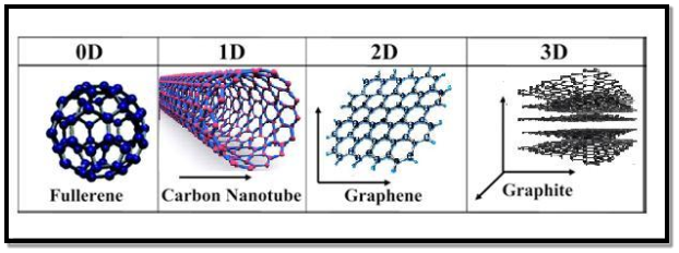
Two-dimensional nanomaterials (2D)
2D nanostructures have two dimensions outside of the nanometric size range. In recent years, a synthesis 2D NSMs have become a focal area in materials research, owing to their many low dimensional characteristics different from the bulk properties. In the search of 2D NSMs, considerable re-search attention has been focused over the past few years on the development of 2D NSMs. 2DNSMs with certain geometries exhibit unique shape-dependent characteristics and subsequent utilization as building blocks for the key components of nanodevices.
In addition, a 2D NSMs are particularly interesting not only for basic understanding of the mechanism of nanostructure growth, but also for investigation and developing novel applications in sensors, photo catalysts, nano-containers, nanoreactors, and templates for 2D structures of other materials.
There are 2D NSMs such as junctions (continuous islands), branched structures, nanoprisms, nanoplates, nanosheets, nanowalls, and nanodisks.
They are basically nanomaterials formed by very thin layers; thin nanolayers with areas of undefined size and a thickness between 1 and 100 nm.
Graphene is the most notable example because, due to its multiple and exceptional properties, it has the potential to revolutionize technology. Its possible applications extend to very diverse areas, ranging from the miniaturization of electronic devices to the elaboration of drugs against cancer in medicine.
Q 8) Write a short note on Carbon nanotubes and also discuss its properties?
A 8)
Carbon nanotubes: Carbon nanotubes were first observed b Sunmino Iijima in 1911. Carbon exists in a large number of allotropic forms. These includes diamond, graphite and fullerenes (such as C60 , C70 etc.,). Carbon nanotubes are obtained by rolling the graphite sheet into tubes with the bonds at the ends of the sheet. These bonds are used to close the tube. Generally, the length of carbon nanotubes varies from several micrometres to millimetre and the diameter will vary from 1 to 20 nm.
A tube may contain one cylindrical wall of graphite or a number of concentric cylindrical walls. A carbon nanotube consisting of one cylindrical graphite is called single walled nanotube. Otherwise they are known as multi walled nanotubes.
Depending on how sheet is rolled, they are classified into three types. The three types of carbon nanotubes are 1) Zigzag 2) Chiral 3) Armchair
Properties
Electrical conductivity: Generally the carbon nanotubes produced both in metallic and semiconducting in their electrical behaviour. Conductivity of multi walled nanotube id more complex. The conductivity and resistivity of ropes of single walled carbon nanotubes has been measured by placing the electrodes at different parts of the carbon nanotubes. The resistivity of single walled carbon nanotube ropes was of the order of 10-4 ohm-cm at 270. This means that the conductivity of single walled nanotube ropes are most conductive carbon fibres of known.
Magnetic property: The carbon nanotube displays the magneto-resistive effects at lower temperature i.e., the resistance of the carbon nanotube is changed by the application of dc magnetic field. The variation of resistance in carbon nanotube at 2.3K and 0.36k w.r.t magnetic field is observed. This show magneto- resistance effect is negative. This is due to the decrease in resistance with increase in magnetic field.
Highly absorbent: The carbon nanotubes have large surface area and high absorbance. So the carbon nanotubes are used in the air, gas and water filtration.
Mechanical properties: The strength of the sp2 carbon-carbon bonds gives carbon nanotubes amazing mechanical properties. The stiffness of the material is measured in terms of its Young’s modulus. The Young’s modulus value of single walled nanotube is about 1Tera Pascal, which is approximately 5 times greater than steel. The tensile strength or breaking strain of nanotube is about 150GPa, which is approximately 150 times greater than steel
Vibration properties: Similar to carbon dioxide molecule, Carbon nanotubes have two normal modes of vibration (a set of vibrational motions known as normal mode of vibrations). The different modes of vibrational motion are determined from the symmetry of the molecule. In the first mode the diameter of the carbon nanotube moves in and out at the frequency of 165 cm-1. In the second mode the carbon nanotube crushing in one direction and expansion takes place in the perpendicular direction. Thus, it oscillates between sphere and ellipse at a frequency of 17 cm-1. The frequency of the vibration modes depends on the diameter of the nanotube.
Q 9) Discuss Single-Walled Carbon Nanotubes (SWNTs) ?
A 9)
Single-Walled Carbon Nanotubes (SWNTs)
Single-wall carbon nanotubes (SWNTs) are a special class of carbon materials known as one-dimensional materials. They consist of sheets of graphene, rolled up to form hollow tubes with walls one atom thick. Due to its chemical structure and dimensional constraints, this material exhibits exceptional mechanical, electrical, thermal, and optical properties. As such, carbon nanotubes have become of great interest for both stand-alone studies and for use in composite materials.
A SWNT can be described as a long tube formed by wrapping a single graphene sheet into a cylinder with diameter of about 1 nanometer, the ends of which are capped by fullerene cages.
The fullerene structures, with alternating structures of five hexagons adjacent to one pentagon, form the surface with desired curvature to enclose the volume. The sidewalls of carbon nanotubes are made of graphene sheets consisting of neighbouring hexagonal cells.
Other polygon structures, such as pentagons and heptagons, constitute defects of sidewalls. The cylindrical sidewalls can be produced from different rolling directions to make SWNTs with distinct structures and properties. Due to cylindrical symmetry, there are only a handful of methods that are effective in making seamless cylinders, and they are characterized by the chiral vectors with integer indices (n, m).
To establish the chiral vector, two atoms in the graphene sheet are selected, with one serving as the origin of the vector pointing toward the other atom. The graphene sheet is then rolled in a way that allows the two atoms to coincide.
Under these circumstances, the chiral vectors form a plane perpendicular to the longitude direction of nanotubes and the lengths of the chiral vectors are equal to the circumference.
Three different types of SWNTs are distinctly characterized, named “zigzag” (m = 0), “armchair” (n = m), and “chiral.” These structural variations result in differences in electrical conductivity and mechanical strength.
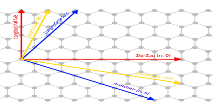
Figure 13
The electrical properties of carbon nanotubes are dependent upon the orientation of the lattice. The lattice orientation is given by two parameters (n, m). The image to the right shows how the n and m orientations relate to the longitudinal axis of the nanotube and the rotational axis. There are typically three types of nanotubes that can form, these are: the armchair (where n = m), zig-zag (n=x, m=0), and chiral (n=x, m=y).

| (n,0) zigzag nanotube
|
 | (n, n) armchair nanotube
|
 | (n, m) chiral nanotube
|
Figure 14
Carbon nanotubes can exhibit either metallic properties or semiconducting properties, depending upon the orientation of the lattice. Zig-zag and armchair carbon nanotubes exhibit metallic properties, whilst chiral nanotubes can be either metallic or semiconducting depending upon the difference between the n and m units.
In addition to this ability to exhibit both metallic and semiconducting electronic structures carbon nanotubes offer exceptional charge carrier mobilities, this is due to the combination of the delocalisation of electrons across the lattice and the small dimensions in the radial axis constraining movement of charge carriers along the longitudinal axis of the tubes.
Q 10) Discuss Double-walled carbon nanotubes (DWCNTs) ?
Double-walled carbon nanotubes (DWCNTs)
A 10)
Double-walled carbon nanotubes (DWCNTs) belong to the family of one-dimensional materials, similar to single-walled carbon nanotubes. This particular class of carbon nanotube consists of two nanotubes, with one nested within the other. The differences in the diameters of the two nanotubes can produce varying degrees of interaction between the two tubes.
DWCNTs consist of two individual carbon nanotubes, with one embedded inside the other. The differences in diameters and the chirality of the two different nanotubes lead to a varying degree of interaction between the two, while at the same time the properties of the individual nanotubes being separate from each other. It is this wide variety of possibilities that have made DWCNTs a focus of interest for carbon nanotube research. Varying chirality allows a range of inner-wall outer-wall interactions to occur, because the chirality determines whether the nanotube will be semiconducting or metallic. It is possible to achieve metallic-metallic, semiconducting-metallic, metallic-semiconducting or semiconducting-semiconducting interactions. In addition to this, the metallic and semiconducting properties can vary depending upon the exact lattice parameters, which enables a wide range of possible property combinations.
DWCNTs also have a large advantage over single-walled carbon nanotubes, as it is possible to modify the outer nanotube without changing the properties of the inner nanotube. This modification could be either through functionalisation (to add solubilising groups), or the doping of the structure (to alter the properties). This allows the double-walled system to maintain functionality of a single-walled nanotube whilst simultaneously having the solubility of functionalised nanotubes. This combination makes double-walled systems attractive for use as additives in composite materials as it allows high doping concentrations without affecting the properties of the nanotube overall.
The biggest barriers for DWCNTs are their synthesis and purification. DWCNTs can be synthesis by arc discharge or catalytic chemical vapour deposition. The remainder of the nanotubes synthesised using these techniques are a mixture of single-walled and multi-walled nanotubes which then need to be purified to obtain individual double-walled nanotubes. The process of purification is much more difficult.
Methods such as high-temperature oxidation result in preferential oxidation of single-walled nanotubes over double-walled. However, the process can damage the remaining nanotubes and will leave residual multi-walled contaminants behind.
Other processes, such as ultra-centrifugation, can be used to obtain high-purity DWCNT samples and sort double-walled samples by outer diameter. However this process is labour and time intensive making commercialisation and large scale production of high purity DWCNTs difficult.
Just like with single-walled carbon nanotubes, there are many different areas in which DWCNT's can be applied due to their impressive mechanical and electrical properties.
In addition double-walled nanotubes show an increase in the mechanical strength, thermal stability, and also chemical stability over that of single-walled nanotubes. However, the ability to combine different nanotube types have the potential to result in interesting optical, electronic and mechanical properties that are not possible with single-walled nanotubes.
Q 11) Discuss Multi-walled carbon nanotubes (MWCNTs)?
A 11)
Multi-walled carbon nanotubes (MWCNTs)
Multi-walled carbon nanotubes (MWCNTs) are a special form of carbon nanotubes in which multiple single-walled carbon nanotubes are nested inside one another. Although MWCNTs are still classed as a 1-dimenional form of carbon, the unique properties that are seen within single-walled and double-walled carbon nanotubes are not as prominent.
MWCNTs consist of multiple carbon nanotubes nested within one another. The number of nanotubes that are within a MWCNT can vary - from as little as 3, to over 20. At the same time the diameter of both the internal nanotube and the external most nanotube can vary - from 2nm for the innermost tube, to over 50nm for the outer wall.
Just like single-walled nanotubes, they exhibit exceptional electrical, thermal, and mechanical properties. However, due to the increased number of walls, there is a higher likelihood of defects being present compared to single-walled nanotubes - resulting in reduced performances. The outer walls of MWCNTs can be modified with functional groups such as hydroxides, carboxylic acids, or amides to produce additional functionality.
MWCNTs can be produced in high quantities and are easier to purify (in comparison to single walled and double-walled nanotubes). This makes their production costs significantly lower, and is a reason for their adoption in multiple areas of scientific research.
Applications of MWCNTs have been mainly focused around their use in composites where they can be used as an additive. Either to:
i) improve the mechanical properties of a material
Ii) To improve the electrical properties of a material.
Aside from being used as additives, functionalised MWCNTs are being utilised in a variety of medical and biotechnological applications. This is due to their high biocompatibility of carbon nanotubes and the ability to attach specific proteins to functional groups. This can provide a wide variety of targeted therapies such as drug delivery, localised heating for triggering cell death, or even miniature biosensors for in-situ measurements.
Q 12) Explain dual nature of matter?
A 12)
As we know in the Photoelectric Effect, the Compton Effect, and the pair production effect—radiation exhibits particle-like characteristics in addition to its wave nature. In 1923 de Broglie took things even further by suggesting that this wave–particle duality is not restricted to radiation, but must be universal.
In 1923, the French physicist Louis Victor de Broglie (1892-1987) put forward the bold hypothesis that moving particles of matter should display wave-like properties under suitable conditions.
All material particles should also display dual wave–particle behaviour. That is, the wave–particle duality present in light must also occur in matter.
So, starting from the momentum of a photon p = hν/c = h/λ.
We can generalize this relation to any material particle with nonzero rest mass. Each material particle of momentum  behaves as a group of waves (matter waves) whose wavelength λ and wave vector
  are governed by the speed and mass of the particle. De Broglie proposed that the wave length λ associated with a particle of momentum p is given as where m is the mass of the particle and v its speed.
λ =  =
= …….(1)
  =
=  …….(2)
Where ℏ = h/2π. The expression known as the de Broglie relation connects the momentum of a particle with the wavelength and wave vector of the wave corresponding to this particle. The wavelength λ of the matter wave is called de Broglie wavelength. The dual aspect of matter is evident in the de Broglie relation.
λ is the attribute of a wave while on the right hand side the momentum p is a typical attribute of a particle. Planck’s constant h relates the two attributes. Equation (1) for a material particle is basically a hypothesis whose validity can be tested only by experiment.
However, it is interesting to see that it is satisfied also by a photon. For a photon, as we have seen, p = hν/c.
Therefore
 =
=  = λ
= λ
Q 13) What is the de Broglie wavelength associated with (a) an electron moving with a speed of 5.4×10⁶ m/s, and (b) a ball of mass 150 g travelling at 30.0 m/s?
A 13)
(a)For the electron:
Mass m = 9.11×10⁻³¹ kg, speed v = 5.4×10⁶ m/s.
Then, momentum
p = m v = 9.11×10–31 kg × 5.4 × 106 (m/s)
p = 4.92 × 10⁻²⁴ kg m/s
De Broglie wavelength, λ = h/p = 6.63 x 10⁻³⁴Js/ 4.92 × 10⁻²⁴ kg m/s
λ= 0.135 nm
(b)For the ball:
Mass m’ = 0.150 kg,
Speed v ’= 30.0 m/s.
Then momentum p’ = m’ v’= 0.150 (kg) × 30.0 (m/s)
p’= 4.50 kg m/s
De Broglie wavelength λ’ = h/p’ =6.63 x 10⁻³⁴Js/ 4.50 kg m/s =1.47 ×10⁻³⁴ m
The de Broglie wavelength of electron is comparable with X-ray wavelengths. However, for the ball it is about 10–19 times the size of the proton, quite beyond experimental measurement.
Q 14) What is the de Broglie wavelength associated with an electron, accelerated through a potential difference of 100 volts?
A 14)
Accelerating potential V = 100 V. The de Broglie wavelength λ is
λ= h /p = 1 227/ nm
nm
λ.1 227/ nm = 0.123 nm
The de Broglie wavelength associated with an electron in this case is of the order of x ray wavelengths.
Q 15) A 45 kW broadcasting antenna emits radio waves at a frequency of 4 MHz.
(a) How many photons are emitted per second?
(b) Is the quantum nature of the electromagnetic radiation important in analyzing the radiation emitted from this antenna?
A 15)
(a) The electromagnetic energy emitted by the antenna in one second is E = 45 000 J. Thus, the number of photons emitted in one second is

(b) Since the antenna emits a huge number of photons every second, 1.7 1031, the quantum nature of this radiation is unimportant. As a result, this radiation can be treated fairly accurately by the classical theory of electromagnetism.
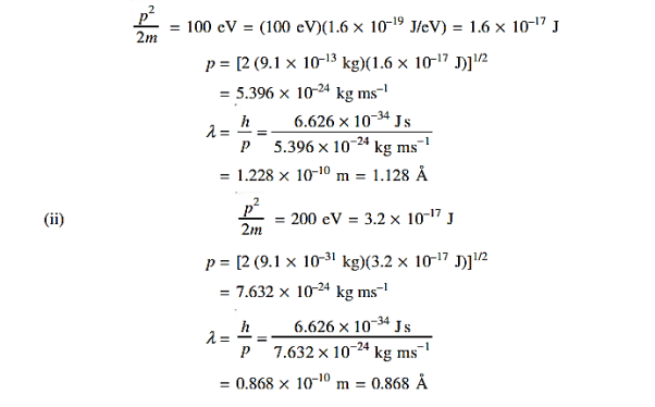
Q 16) Determine the de Broglie wavelength of an electron that has been accelerated through a potential difference of (i) 100 V, (ii) 200 V.
A 16)
(i)The energy gained by the electron = 100 eV. Then
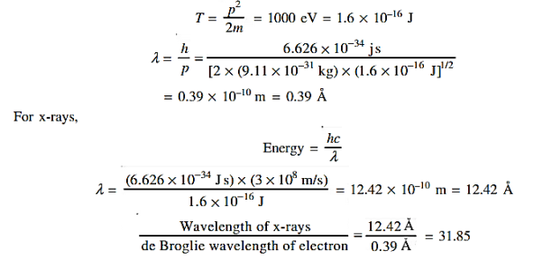
Q 17) Calculate the de Broglie wavelength of an electron having a kinetic energy of 1000 eV. Compare the result with the wavelength of x-rays having the same energy?
A 17)
The kinetic energy
