Question Bank
Unit 3
Q .1. Explain Hall Effect in detail?
Answer:
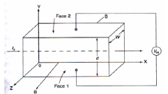
When a material carrying current is subjected to a magnetic field in a direction perpendicular to direction of current, an electric field is developed across the material in a direction perpendicular to both the direction of magnetic field and current direction. This phenomenon is called “Hall-effect”.
Explanation:
* Consider a semi-conductor, and current passes along the X-axis and a magnetic field Bz is applied along the Z-direction, a field Ey is called the Hall field which is developed in the Y-direction.
* In P- type semi-conductor, holes move with the velocity “V” in the “+”ve X-direction. As they move across the semiconductor the holes experience a transverse force ‘Bev’ due to the magnetic field.
* This force drives the holes down to the lower face. As a result, the lower face becomes +vely charged and –ve charge on the upper surface creating the hall field in the Y-direction. The Hall field exerts an upward force on holes equal to Ee.
* In the steady sate, two forces just balance and as a result, no further increase of + ve charge occurs on Face1.
* In N type semiconductor, the majority charge carriers are electrons experiences a force in the downward direction and lower face gets – vely charged. As a result, Hall field will be in the Y – direction.
Hall Coefficient:
Hall field𝐸𝐻, for a given material depends on the current density J and the applied magnetic field B.
i.e. 𝐸𝐻α JB
𝐸𝐻 = 𝑅𝐻 α JB
Since,
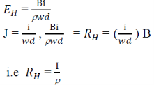
This is called hall coefficient.
Q.2 Explain zener diode?
Answer:
A Zener diode is a silicon semiconductor device that permits current to flow in either a forward or reverse direction. The diode consists of a special, heavily doped p-n junction, designed to conduct in the reverse direction when a certain specified voltage is reached.
The Zener diode has a well-defined reverse-breakdown voltage, at which it starts conducting current, and continues operating continuously in the reverse-bias mode without getting damaged. Additionally, the voltage drop across the diode remains constant over a wide range of voltages, a feature that makes Zener diodes suitable for use in voltage regulation.
The Zener diode operates just like the normal diode when in the forward-bias mode, and has a turn-on voltage of between 0.3 and 0.7 V. However, when connected in the reverse mode, which is usual in most of its applications, a small leakage current may flow. As the reverse voltage increases to the predetermined breakdown voltage (Vz), a current starts flowing through the diode. The current increases to a maximum, which is determined by the series resistor, after which it stabilizes and remains constant over a wide range of applied voltage.
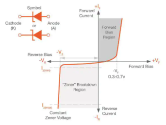
Zener breakdown
The breakdown is either due to the Zener breakdown effect that occurs below 5.5 V, or impact ionization that occurs above 5.5 V. Both mechanisms result in the same behaviour and do not require different circuitry; however, each mechanism has a different temperature coefficient.
The Zener effect has a negative temperature coefficient while the impact effect experiences a positive coefficient. The two temperature effects are almost equal at 5.5 V and cancel out each other to make the Zener diodes rated at around 5.5 V the most stable over a wide range of temperature conditions
Q.3 Explain kronig- penny model?
Answer:
According to quantum free electron theory of metals, a conduction electron in a metal experiences constant (or zero) potential and free to move inside the crystal but will not come out of the metal because an infinite potential exists at the surface. This theory successfully explains electrical conductivity, specific heat, thermionic emission and Para magnetism. This theory is fails to explain many other physical properties, for example:
(i) it fails to explain the difference between conductors, insulators and semiconductors,
(ii) positive Hall coefficient of metals and
(iii) lower conductivity of divalent metals than monovalent metals.
To overcome the above problems, the periodic potentials due to the positive ions in a metal have been considered. If an electron moves through these ions, it experiences varying potentials. The potential of an electron at the positive ion site is zero and is maximum in between two ions. The potential experienced by an electron, when it passes along a line through the positive ions.
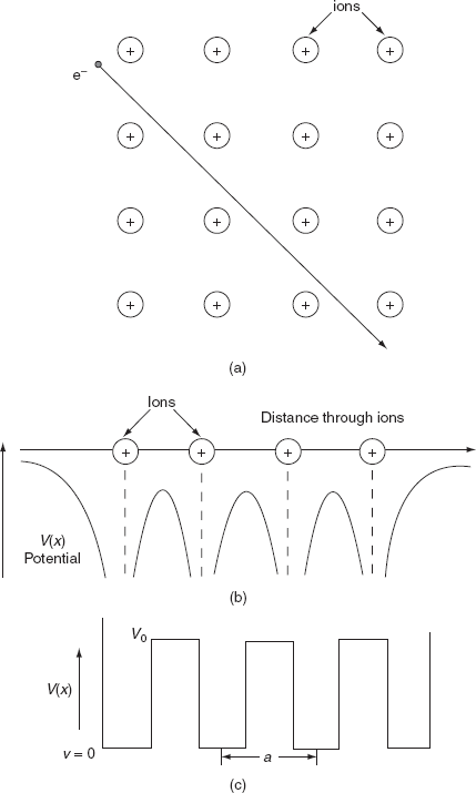
It is not easy to solve Schrödinger’s equation with these potentials. So, Kronig and Penney approximated these potentials inside the crystal to the shape of rectangular steps as shown in Fig. (c). This model is called Kronig-Penney model of potentials.

The energies of electrons can be known by solving Schrödinger’s wave equation in such a lattice. The Schrödinger time-independent wave equation for the motion of an electron along X-direction is given by:
 ...............(1)
The energies and wave functions of electrons associated with this model can be calculated by solving time-independent one-dimensional Schrödinger’s wave equations for the two regions I and II as shown in Fig
The Schrödinger’s equations are:
 for 0<x<a.............(2)
 for -b<x<0.............(3)
We define two real quantities (say) α and β such that:

Hence, becomes:
 for 0<x<a
 for -b<x<0
According to Bloch's theorem, the wavefunction solution of the Schrödinger equation when the potential is periodic and to make sure the function u(x) is also continuous and smooth, can be written as:

Where u(x) is a periodic function which satisfies u (x + a) = u(x).
Using Bloch theorem and all the boundary conditions for the continuity of the wave function the solution of Schrodinger wave equation obtained as

Where 
This equation shows the relation between the energy (through α) and the wave-vector, k, and as you can see, since the left hand side of the equation can only range from −1 to 1 then there are some limits on the values that α (and thus, the energy) can take, that is, at some ranges of values of the energy, there is no solution according to these equation, and thus, the system will not have those energies
Q. 4 Explain Energy density state?
Answer:
The density of states in a semiconductor equals to the number of states per unit energy and per unit volume.
Calculation of Density of states
We will assume that the semiconductor can be modelled as an infinite quantum well in which electrons with effective mass, m*, are free to move. The energy in the well is set to zero. The semiconductor is assumed a cube with side L.
This assumption does not affect the result since the density of states per unit volume should not depend on the actual size or shape of the semiconductor.
Consider a sphere in k-space. Associated with this sphere volume will be

Where k is our “radius" where

We now define a state by the smallest nonzero volume it possesses in k-space. This occurs when

A cube in k-space with size L (Lx = Ly = Lz =L) as indicated on Figure


Thus, within our imagined spherical volume of k-space, the total number of states present is


Next, when dealing with electrons and holes, we must consider spin degeneracy, since two carriers, possessing opposite spin, can occupy the same state. As a consequence, we multiply the above expression by 2 to obtain

Q 5 Explain Free electron theory of metal?
Answer:
According to this theory, a metal consists of electrons which are free to move about in the crystal-like molecules of a gas in a container. Mutual repulsion between electrons is ignored and hence potential energy is taken as zero. Therefore, the total energy of the electron is equal to its kinetic energy. This model provided a satisfactory explanation for certain properties (e.g., electrical conductivity, electronic emission and electronic emission) but failed to explain that why some solids are good Conductor some are Semiconductor and other are insulators. It also fails to explain the specific heat of metals and magnetic susceptibility of paramagnetic metals.
This theory was developed by Drude and Lorentz and hence is also known as Drude-Lorentz theory.
Postulates of free electron Model
1. The outermost electrons of the constituent atom of the metal are weakly bound with the atoms. Hence these electrons get separated from their atoms and move freely inside the substance and are called free electrons.
2. There are large number of free electrons inside the metals and hey behave like molecules of a gas enclosed in a container. Hence it is called free electron gas. These free electrons are responsible for the thermal and electrical conduction inside the metal. Hence, they are also called conduction electrons.
3.The free electrons in thermal equilibrium obey Maxwell-Boltzmann statistics. Which states that the free energy per electron at an absolute temperature T is 1/2 KT, where K is Boltzmann's constant.
4. Inside the metal, free electrons move randomly with high velocity and it depends on the temperature of the metal. During the motion, their velocity and direction changes in such a way that the rate of flow of electron in a particular direction is zero.
5. When the metal is kept in external electric field, the free electrons gets attracted in the direction opposite to the direction to the external electric field. They start moving with a constant average velocity called drift velocity.
Q 6 Describe Fermi level in Extrinsic Semiconductor?
Answer:
In extrinsic semiconductor, the number of electrons in the conduction band and the number of holes in the valence band are not equal. Hence, the probability of occupation of energy levels in conduction band and valence band are not equal. Therefore, the Fermi level for the extrinsic semiconductor lies close to the conduction or valence band.
Fermi level in n-type semiconductor
In n-type semiconductor pentavalent impurity is added. Each pentavalent impurity donates a free electron. The addition of pentavalent impurity creates large number of free electrons in the conduction band.
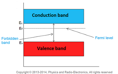
At room temperature, the number of electrons in the conduction band is greater than the number of holes in the valence band. Hence, the probability of occupation of energy levels by the electrons in the conduction band is greater than the probability of occupation of energy levels by the holes in the valence band. This probability of occupation of energy levels is represented in terms of Fermi level. Therefore, the Fermi level in the n-type semiconductor lies close to the conduction band.
The Fermi level for n-type semiconductor is given as

Where EF is the fermi level.
EC is the conduction band.
KB is the Boltzmann constant.
T is the absolute temperature.
NC is the effective density of states in the conduction band.
ND is the concentration of donar atoms.
Fermi level in p-type semiconductor
In p-type semiconductor trivalent impurity is added. Each trivalent impurity creates a hole in the valence band and ready to accept an electron. The addition of trivalent impurity creates large number of holes in the valence band.
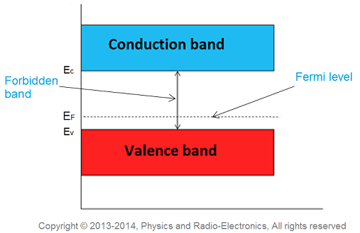
At room temperature, the number of holes in the valence band is greater than the number of electrons in the conduction band. Hence, the probability of occupation of energy levels by the holes in the valence band is greater than the probability of occupation of energy levels by the electrons in the conduction band. This probability of occupation of energy levels is represented in terms of Fermi level. Therefore, the Fermi level in the p-type semiconductor lies close to the valence band.
The Fermi level for p-type semiconductor is given as

Where NV is the effective density of states in the valence band.
NA is the concentration of acceptor atoms.
Q 7 In Periodic potential Explain Bloch Theorem?
Answer:
The Bloch theorem in essence formulates a condition that all solutions ψk(r), for any periodic potential V(r) whatsoever, have to meet. In one version it ascertains

With k = any allowed wave vector for the electron that is obtained for a constant potential, and uk(r) = arbitrary functions (distinguished by the index k that marks the particular solution we are after), but always with the periodicity of the lattice, i.e.

Any wavefunction meeting this requirement we will henceforth call a Bloch wave
The Bloch theorem is quite remarkable, because, as said before, it imposes very special conditions on any solution of the Schrödinger equation, no matter what the form of the periodic potential might be.
We notice that exactly as in the case of the constant potential, the wave vector k has a twofold role: It is still a wave vector in the plane wave part of the solution, but also an index to ψk(r) and uk(r) because it contains all the quantum numbers, which enumerate the individual solutions.
Bloch's theorem is a proven theorem with perfectly general validity. We will first give some ideas about the proof of this theorem, and then discuss what it means for real crystals. As always with hindsight, Bloch's theorem can be proved in many ways
It can be proved (and used for further calculations), by expanding V(r) and ψ(r) into a Fourier series and then rewriting the Schrödinger equation. This is a particularly useful way because it can also be used for obtaining specific results for the periodic potential
Bloch's theorem can also be rewritten in a somewhat different form, giving us a second version:

This means that any function ψk(r) that is a solution to the Schrödinger equation of the problem, differs only by a phase factor exp(ikT) between equivalent positions in the lattice
This implies immediately that the probability of finding an electron is the same at any equivalent position in the lattice, exactly as we expected, because

This is so because |exp(ikT)|2 = 1 for all k and T.
If we write the wave function in the first form ψk(r) = uk(r) · exp(ikr) and consider its value at an equivalent lattice position r + T we obtain |
|

Q 8 Explain Fermi level In Intrinsic Semiconductor?
Answer:
The probability of occupation of energy levels in valence band and conduction band is called Fermi level. At absolute zero temperature intrinsic semiconductor acts as perfect insulator. However as the temperature increases free electrons and holes gets generated.
In intrinsic or pure semiconductor, the number of holes in valence band is equal to the number of electrons in the conduction band. Hence, the probability of occupation of energy levels in conduction band and valence band are equal. Therefore, the Fermi level for the intrinsic semiconductor lies in the middle of forbidden band.
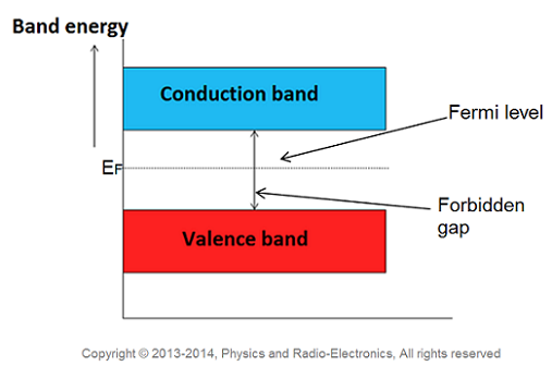
Fermi level in the middle of forbidden band indicates equal concentration of free electrons and holes.
The hole-concentration in the valence band is given as

The electron-concentration in the conduction band is given as

Where KB is the Boltzmann constant
T is the absolute temperature of the intrinsic semiconductor
Nc is the effective density of states in the conduction band.
Nv is the effective density of states in the valence band.
For an intrinsic semiconductor, the electron-carrier concentration is equal to the hole-carrier concentration.
It can be written as
p = n = ni
Where P = hole-carrier concentration
n = electron-carrier concentration
And ni = intrinsic carrier concentration
The fermi level for intrinsic semiconductor is given as,

Where EF is the fermi level
EC is the conduction band
EV is the valence band
Therefore, the Fermi level in an intrinsic semiconductor lies in the middle of the forbidden gap
Q 9 Explain working of Solar Cell?
Answer:
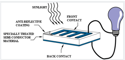
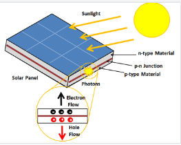
A solar panel works by allowing photons, or particles of light, to knock electrons free from atoms, generating a flow of electricity. Solar panels actually comprise many, smaller units called photovoltaic cells. (Photovoltaic simply means they convert sunlight into electricity.) Many cells linked together make up a solar panel
Photovoltaic cells, through the photovoltaic effect, absorb sunlight and generate flowing electricity. This process varies depending on the type of solar technology, but there are a few steps common across all solar photovoltaic cells.
Step 1: Light is absorbed by the PV cell and knocks electrons loose
First, light strikes a photovoltaic cell and is absorbed by the semiconducting material it is made from (usually silicon). This incoming light energy causes electrons in the silicon to be knocked loose, which will eventually become the solar electricity you can use in your home.
Step 2: Electrons begin to flow, creating an electrical current
There are two layers of silicon used in photovoltaic cells, and each one is specially treated, or “doped”, to create an electric field, meaning one side has a net positive charge and one has a net negative charge. This electric field causes loose electrons to flow in one direction through the solar cell, generating an electrical current.
Step 3: The electrical current is captured and combined with other solar cells
Once an electrical current is generated by loose electrons, metal plates on the sides of each solar cell collect those electrons and transfer them to wires. At this point, electrons can flow as electricity through the wiring to a solar inverter and then throughout your home.
Q 10 Draw V-I Characteristic graph for PN junction?
Answer:
Forward V-I characteristics of p-n junction diode
If the positive terminal of the battery is connected to the p-type semiconductor and the negative terminal of the battery is connected to the n-type semiconductor, the diode is said to be in forward bias. In forward biased p-n junction diode, VF represents the forward voltage whereas IF represents the forward current.
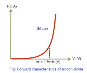
Forward V-I characteristics of silicon diode
If the external voltage applied on the silicon diode is less than 0.7 volts, the silicon diode allows only a small electric current. However, this small electric current is considered as negligible.
Reverse V-I characteristics of p-n junction diode
If the negative terminal of the battery is connected to the p-type semiconductor and the positive terminal of the battery is connected to the n-type semiconductor, the diode is said to be in reverse bias. In reverse biased p-n junction diode, VR represents the reverse voltage whereas IR represents the reverse current.
If the external reverse voltage applied on the p-n junction diode is increased, the free electrons from the n-type semiconductor and the holes from the p-type semiconductor are moved away from the p-n junction. This increases the width of depletion region.
The wide depletion region of reverse biased p-n junction diode completely blocks the majority charge carrier current. However, it allows the minority charge carrier current. The free electrons (minority carriers) in the p-type semiconductor and the holes (minority carriers) in the n-type semiconductor carry the electric current. The electric current, which is carried by the minority charge carriers in the p-n junction diode, is called reverse current