Unit - 1
Introduction to Microcontroller
Q1) Explain the main features of 8-bit microcontroller?
A1)
Characteristics 8-bit microcontroller with an integrated CAN module
1. A 32 k flash program memory,
2. A 1536-byte RAM data memory,
3. A 256-byte EEPROM memory,
4. Twenty two I/O ports,
5. Five-channel 10-bit A/D converters,
6. Three timers/counters,
7. Three external interrupt pins,
8. High current (25-mA) sink/source,
9. Capture/compare/Pulse Width Modulation (PWM) module,
10. SPI/I2C module,
11. CAN 2.0A/B module,
12. Power-on reset and power-on timer,
13. Watchdog timer,
14. Priority level interrupts,
15. DC to 40-MHz clock input,
16. An 8 × 8 hardware multiplier,
17. Wide operating voltage (2.0–5.5 V),
18. Power saving sleep mode.
Q2) Explain features of 16-bit microcontroller?
A2)
CPU16
1. 16 Bit Architecture
2. Control-Oriented Digital Signal Processing Capability
3. 16 bit Multiply and Accumulate (digital signal processing)
4. 1 Megabyte of Program Memory Space and 1 Megabyte of Data Memory Space
5. High Level Language Support
6.Fast Interrupt Response Time
7. Hardware Breakpoint Signal
8. Background Debugging Mode (BDM)
9. Fully Static Operation
10. Watchdog Timer, Clock Monitor and Bus Monitor
11. Parallel Ports Option on Address and Data Bus in Single Chip Mode
12. Two 8 bit Dual Function Input/Output Ports
13. One 7 bit Dual Function Output Port
14. Phase-Locked Loop (PLL) Clock System
15. Multichannel Communication Interface (MCCI)
17. Two channels of enhanced Serial Communication Interface (SCI) (UART)
18. One channel of Serial Peripheral Interface (SPI)
19. Configurable Timer Module Version 7 (CTM7)
20. One 16 bit modulus counters (MCSM)
21. One 16 Bit Free-Running Counter (FCSM)
22. Six single-action submodules (SASM)
Q3) Explain the architecture of 8051 microcontroller?
A3)

Figure 1. 8051 Architecture
Central Processor Unit (CPU)
The brain of any processing device of the microcontroller is the CPU. It monitors and controls all operations performed on these units. It reads program written in ROM memory, executes and does the expected task.
Interrupts
Interrupt is a subroutine call that interrupts the microcontrollers main operations or work and causes it to execute any other program, at the time of operation. It provides a mechanism to put on hold the ongoing operations, execute a subroutine and resume to another type of operation.
8051 has five interrupt sources:
INTO
TFO
INT1
TF1
R1/T1
(INT0) ̅ and (INT1) ̅ are external interrupts negative edge triggered or low level triggered. When these interrupts are activated, the corresponding flags are set except for serial interrupt.
When the processor branches to ISR the interrupt flags are cleared. The external interrupts are timer and serial port interrupts.
Memory
They require memory to save as well as read so that the microcontroller performs specific operations of the task.
The memory which is used to store the program known as code memory or Program memory It is also known as ROM memory.
8051 data memory is used to storing data temporarily for operation known as RAM memory. It has 4K of code memory or program memory and 128 bytes of data memory of RAM.
BUS
A collection of wires that work as communication channel or medium for transfer of data. It consists of 8, 16 or more wires of microcontroller. Thus, they carry 8 bits or 16 bits of data simultaneously. There are two types of buses which are
Address Bus
Data Bus
Address Bus:
Microcontroller 8051 has a 16-bit address bus for transferring data. It addresses memory locations to transfer address from CPU to Memory. It has four addressing modes that are:
Immediate addressing modes.
Bank address (or) Register addressing mode.
Direct Addressing mode.
Register indirect addressing mode.
Data Bus: Microcontroller 8051 has 8 bits of data bus used to carry data for applications.
Oscillator
The 8051 microcontroller has an on-chip oscillator that acts as a clock source for CPU of microcontroller. The output pulses of the oscillator are stable. Therefore, it enables synchronized work for all the parts of Microcontroller system.
Input/output Port
To control the operation of machines microcontroller is used in embedded systems. To connect to other machines, devices or peripherals I/O interfacing ports is required. Microcontroller 8051 has 4 input and output ports to connect to other peripherals
Timers/Counters
8051 microcontroller has two 16-bit timers and counters. The counters are again divided into 8-bit register. Timers are used for measurement of time intervals to determine pulse width.
Q4) What are Special function registers, explain SRF map?
A4)
Registers are known as data storage devices. There are two registers namely Register A and Register B. Register A is used as an accumulator and Register B as general -purpose register. The output of mathematical and logical instructions is stored in these registers.
The operations of addition, subtraction, multiplication and division are performed by Register A. Register B is for multiplication and division which are carried by Register A. For data transfers between microcontroller and external memory Register A is involved.
8051 microcontrollers also has 7 Special Function Registers (SFRs). They are:
1. Serial Port Data Buffer (SBUF)
2. Timer/Counter Control (TCON)
3. Timer/Counter Mode Control (TMOD)
4. Serial Port Control (SCON)
5. Power Control (PCON)
6. Interrupt Priority (IP)
7. Interrupt Enable Control (IE)
Internal Data Memory and Special Function Register (SFR) Map

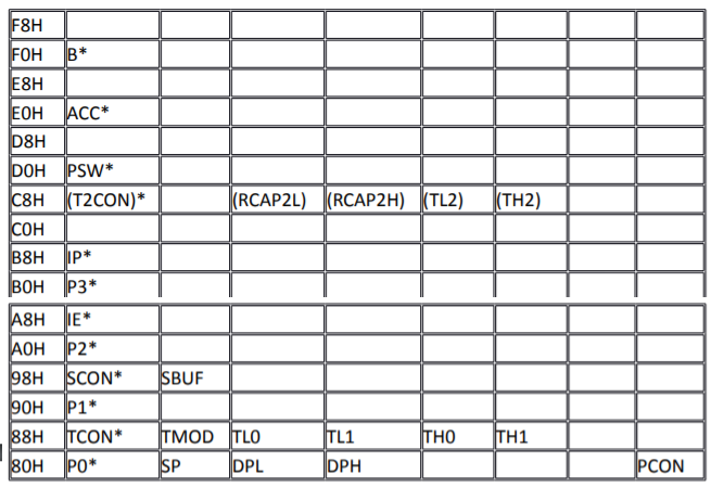
The special function registers (SFRs) are mapped in the upper 128 bytes of internal data memory address. Hence there is an address overlap between the upper 128 bytes of data RAM and SFRs. Please note that the upper 128 bytes of data RAM are present only in the 8052 family. The lower128 bytes of RAM (00H - 7FH) can be accessed both by direct or indirect addressing while the upper 128 bytes of RAM (80H - FFH) are accessed by indirect addressing. The SFRs (80H - FFH) are accessed by direct addressing only. This feature distinguishes the upper 128 bytes of memory from the SFRs, as shown in figure above.
SFR Map
The set of Special Function Registers (SFRs) contains important registers such as Accumulator, Register B, I/O Port latch registers, Stack pointer, Data Pointer, Processor Status Word (PSW) and various control registers. Some of these registers are bit addressable (they are marked with a * in the diagram below). The detailed map of various registers is shown in the following figure.
Q5) Explain the PCON and SCON register with all its bits?
A5)
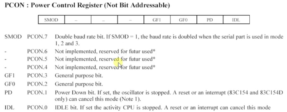
Peripheral Control Registers PCON (Power Control)
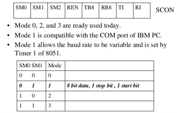
The PCON or Power Control register, as the name suggests is used to control the 8051 Microcontroller’s Power Modes and is located at 87H of the SFR Memory Space. Using two bits in the PCON Register, the microcontroller can be set to Idle Mode and Power Down Mode. During Idle Mode, the Microcontroller will stop the Clock Signal to the ALU (CPU) but it is given to other peripherals like Timer, Serial, Interrupts, etc. In order to terminate the Idle Mode, you have to use an Interrupt or Hardware Reset. In the Power Down Mode, the oscillator will be stopped and the power will be reduced to 2V. To terminate the Power Down Mode, you have to use the Hardware Reset. Apart from these two, the PCON Register can also be used for few additional purposes. The SMOD Bit in the PCON Register is used to control the Baud Rate of the Serial Port. There are two general purpose Flag Bits in the PCON Register, which can be used by the programmer during execution.

SCON (Serial Control)
The Serial Control or SCON SFR is used to control the 8051 Microcontroller’s Serial Port. It is located as an address of 98H. Using SCON, you can control the Operation Modes of the Serial Port, Baud Rate of the Serial Port and Send or Receive Data using Serial Port. SCON Register also consists of bits that are automatically SET when a byte of data is transmitted or received.
Q6) Explain TMOD and TCON registers?
A6)
TCON (Timer Control)
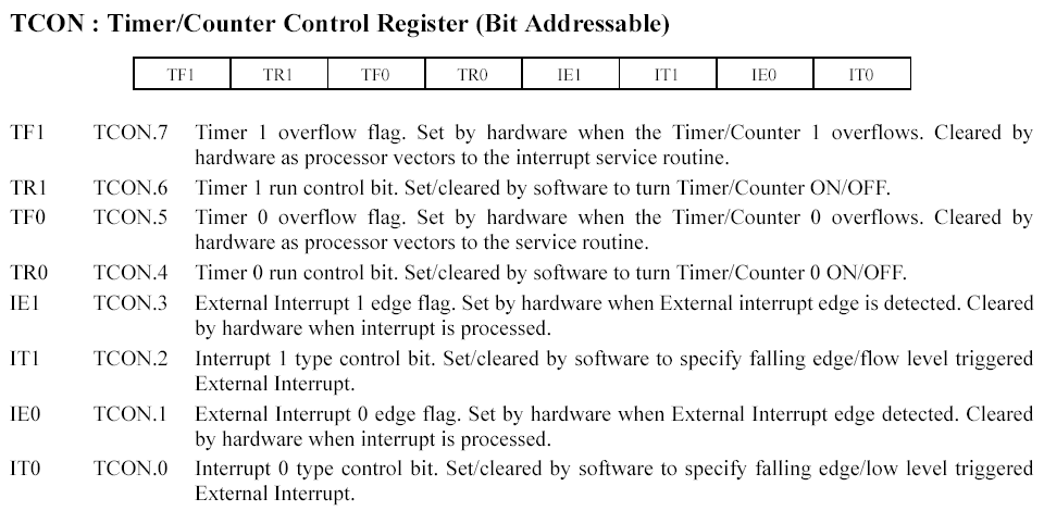
Timer Control or TCON Register is used to start or stop the Timers of 8051 Microcontroller. It also contains bits to indicate if the Timers has overflowed. The TCON SFR also consists of Interrupt related bits.
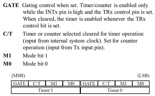
TMOD (Timer Mode)
The TMOD or Timer Mode register or SFR is used to set the Operating Modes of the Timers T0 and T1. The lower four bits are used to configure Timer0 and the higher four bits are used to configure Timer1.

Q7) What is IP register explain all its bits?
A7)
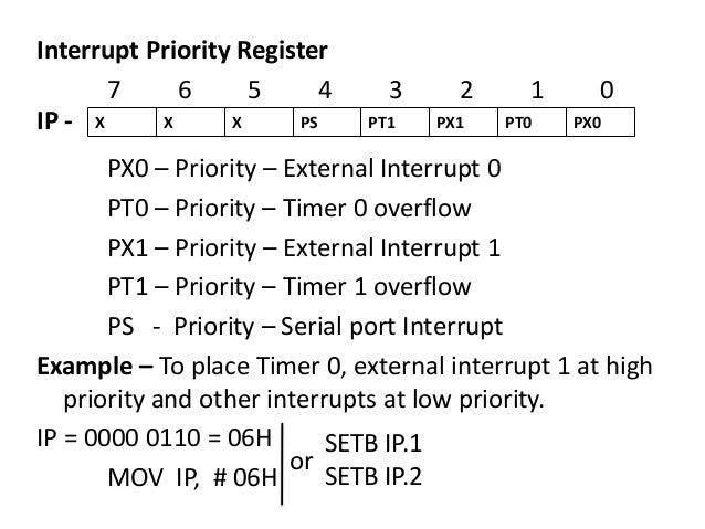
IP (Interrupt Priority)
The IP or Interrupt Priority Register is used to set the priority of the interrupt as High or Low. If a bit is CLEARED, the corresponding interrupt is assigned low priority and if the bit is SET, the interrupt is assigned high priority.

Peripheral Data Registers SBUF (Serial Data Buffer)
The Serial Buffer or SBUF register is used to hold the serial data while transmission or reception.
Q8) What is the clock frequency of 8051? Explain the clock and reset circuit?
A8)
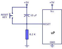
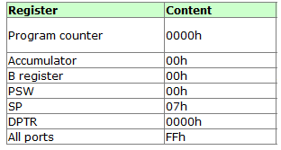
RESET is an active High input when RESET is set to High, 8051 goes back to the power on state. 8051 is reset by holding the RST high for at least two machine cycles and then returning it low.
There are two methods of reset circuit:
1.Power On Reset.
- Initially charging of capacitor makes RST High
- When capacitor charges fully it blocks DC.
2.Manual Reset
- Closing the switch momentarily will make RST High.

After a reset, the program counter is loaded with 0000H but the content of on-chip RAM is not affected.

Clock Circuit
- The 8051 uses the crystal for precisely that to synchronize it’s operation. Effectively, the 8051 operates using what are called "machine cycles."
- A single machine cycle is the minimum amount of time in which a single 8051 instruction can be executed. Although many instructions take multiple cycles.
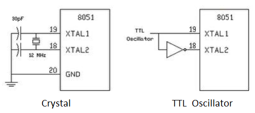
- 8051 has an on-chip oscillator. It needs an external crystal that decides the operating frequency of the 8051.
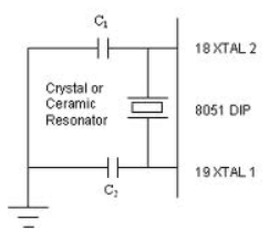
- The crystal is connected to pins 18 and 19 with stabilizing capacitors. 12 MHz (11.059MHz) crystal is often used and the capacitance ranges from 20pF to 40pF.
- The oscillator can also be a TTL clock source connected with a NOT gate as shown.

Q9) Explain the register banks of 8051 along with memory locations?
A9)
A total of 32 bytes of RAM are set aside for the register banks and stack. These 32 bytes are divided into 4 banks of registers in which each bank has 8 registers, RO - R7. RAM locations from 0 to 7 are set aside for bank 0 after RO - R7 where RO is RAM location 0, RI is RAM location I, R2 is location 2, and so on, until memory location 7, which belongs to R7 of bank O. The second bank of registers RO - R7 starts at RAM location 08 and goes to location OFH. The third bank of RO - R7 starts at memory location 10H and goes to location
17H. Finally, RAM locations 18H to 1FH arc set aside for the fourth bank of RO- R7. The following shows how the 32 bytes are allocated into 4 banks
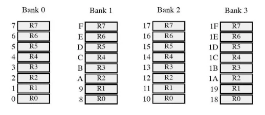
As we see from above the bank uses the same RAM space as the stack. This IS a major problem in programming the 8051. We must either not use register bank I, or allocate another area of RAM for the stack.
Q10) Explain the concept of stack in 8051?
A10)
The stack is a section of RAM used by the CPU to store information temporarily. This information could be data or an address. The CPU needs this storage area since there are only a limited number of registers.
If the stack is a section of RAM, there must be registers inside the CPU to point to it. The register used to access the stack is called the SP (stack pointer) register. The stack pointer in the 8051 is only 8 bits wide, which means that It can take values of 00 to FFH. When the 8051 is powered up, the SP register contains value 07. This means that RAM location 08 is the first location used for the stack by the 8051. The storing of a CPU register in the stack is called a PUSH, and pulling the contents off the stack back into a CPU register is called a POP. In other words, a register is pushed onto the stack to save it and popped off the stack to retrieve it. The job of the SP is very critical when push and pop actions arc performed. To see how the stack works, let's look at the PUSH and POP instructions.
Q11) Explain the effect of PUSH instruction on stack?
A11)
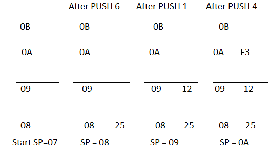
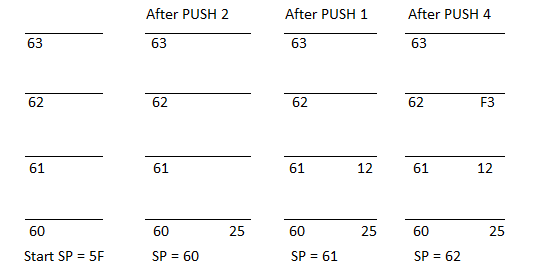
In the 8051 the stack pointer (SP) points to the last used location of the stack. As we push data onto the stack, the stack pointer (SP) is incremented by one. Notice that this is different from many microprocessors, notably x86 processors in which the SP is decremented when data is pushed onto the stack. Examining Example, we see that as each PUSH is executed, the contents of the register arc saved on the stack and SP is incremented by I. Notice that for every byte of data saved on the stack, SP IS incremented only once. Notice also that to push the registers onto the stack we must use their RAM addresses. For example the instruction "PUSH1" pushes register R1 onto the stack
Show the stack and stack pointer for the following. Assume the default stack area and register 0 is selected.
MOV R6,#25H
MOV Rl,#12H
MOV R4,#OF3H
PUSH 6
PUSH 1
PUSH 4
Q12) Explain the execution of CALL instruction with help of any program?
A12)
In addition to using the stack to save registers, the CPU also uses the stack to save the address of the instruction just below the CALL instruction. This is how the CPU knows where to resume when it returns from the called subroutine.
Show the stack and stack pointer for the following instructions,
MOV SP, #5FH; make RAM location 60H
MOV R2, #25H; first stack location
MOV Rl, #12H
MOV R4, #OF3H
PUSH 2
PUSH 1
PUSH 4

Q13) What is Program Counter? Explain step by step execution of a program byte by byte?
A13)
Another important register in the 8051 is the PC (program counter). The program counter points to the address of the next instruction to be executed. As the CPU fetches the opcode from the program ROM, the program counter is incremented to point to the next instruction. The program counter in the 8051 is 16 bits wide. This means that the 8051 can access program addresses 0000 to FFFFH, a total of 64K bytes of code. However, not all members of the 8051 have the entire 64K bytes of on-chip ROM installed.
Program Counter (PC) – 16 bit PC contains the address of next instruction to be executed. On reset PC will set to 0000. After fetching every instruction PC will increment by one.
When the 8051 is powered up, the PC (program counter) has the value of 0000 in it. This means that it expects the first opcode to be stored at ROM address OOOOH. For this reason, in the 8051 system, the first opcode must be burned into memory location OOOOH of program ROM since this is where it looks for the first instruction when it is booted. We achieve. This by the ORG statement in the source program as shown earlier.
Executing a program byte by byte
Assuming that the above program is burned into the ROM of an 8051 chip (or 8751, AT895I, or DS5000), the following is a step-by-step description of the action of the 8051 upon applying power to it.
I. When the 8051 is powered up, the PC (program counter) has 0000 and starts to fetch the first opcode from location 0000 of the program ROM. In the case of the above program the first opeode is 70, which is the code for moving an operand to R5. Upon executing the opcode, the CPU fetches the value 25 and places it in R5. Now once instruction is finished. Then the program counter is incremented to point to 0002 (PC = 0002), which contains opcode 7F, the opcode for the instruction "MOV R7".
2. Upon executing the opcode 7F, the value 34H is moved into R7. Then the program counter is incremented to 0004.
3. ROM location 0004 has the opcode for the instruction "MOV A, #0". This instruction is executed and now PC = 0006. Notice that all the above instructions arc 2-byte instructions; that is, each one takes two memory locations.
4. Now PC = 0006 points to the next instruction, which is "ADD A, RS". This is a l-byte instruction. After the execution of this instruction, PC = 0007.
5. The location 0007 has the opcode 2F, which belongs to the instruction "ADD A, R7". This also is a l-byte instruction. Upon execution of this instruction PC is incremented to 0008. This process goes on until all the instructions are fetched. And executed. The fact that the program counter points at the next instruction to be executed explains why some microprocessors (notably the x86) call the program counter the ins/ruction pointer.
Q14) Explain port structure of 8051?
A14)
Port Structure
8051 has four ports P0, P1, P2, P3. They are required for I/O operations.
32 pins are set for four ports P0,P1,P2,P3. Each port takes 8 pins.
All the ports are configured as input upon Reset
When zero is written to port it becomes output. To make it input 1 needs to be sent to the port.
Port 0:
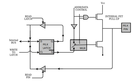
Fig 2. Port -0
When Port0 is used as input port 1 must be written to the corresponding zero latch that causes the output transistor to switch off and pin floats in high impedance state.
When configured as input port it provides two facilities:
Reads logic level on physical pin by asserting read pin signal.
Read contents of internal latch by asserting the read latch signal.
The latch is read for instruction read-modify-write type instruction.
It reads data from the port modifies and writes to the port.
When Port0 is configured as output the latch pins that are programmed to 0 will cause the lower FET to turn ON and pin is grounded.
If 1 is written to the latch pin FET will turn OFF and pin is pulled HIGH by external pull-up resistor.
Port 1:
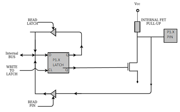
Figure 3. Port 1 circuit
When port 1 is used as in input port ‘1’ must be written to the corresponding port1 latch bit. This causes the lower FET to turn off.
The pin and the input buffer are pulled to logic HIGH by internal pull load.
This port is called quasi-bidirectional port because its output is pulled high with pull up resistor.
When port 1 is used as an output port, the latch pins that are programmed to 0, will cause the lower FET turn on the internal pull to turn off and input is logic 0.
If 1 is written onto the latch, then it will drive the input of external circuit high through pull up. The lower FET turns off.
Port 2:

Figure 4. Port 2 circuit
When Port2 is used as an input port 1 must be written to the corresponding latch bit. This cause the FET turn off. The pin and input to pin buffer are pulled to logic high by internal pull up load.
Port 2 is called as “quasi-bidirectional port” as its output is pull up resistors.
When port2 is used as output port the latch pins that are programmed to 0, will cause the lower FET to turn off and input to the circuit logic 0.
If “1” is written onto latch pin, then it will drive the input of external circuit high through pull-up. The lower FET turns off.
Port 3:

Figure 5. Port 3 circuit

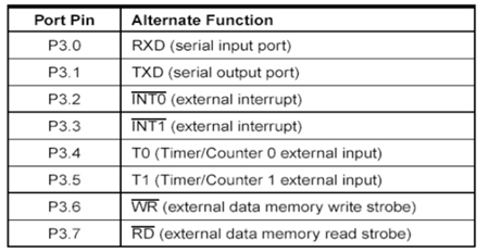
When port3 is used as input port 1 must be written to the corresponding port3 latch bit.
This causes FET to turn off.
The pin and input to the buffer are pulled to logic HIGH by internal pull up load.
When port3 is used as output port, the latched pins that are programmed to 0 will cause to lower FET to turn on and internal pull up to turn off and input to circuit is logic 0.
If 1 is written onto latch pin it will drive the input external circuit high through pull up. The lower FET turns off.
Q15) Explain the Data memory of 8051 microcontroller?
A15)
Data Memory or RAM stores temporary data and intermediate results generated during the normal operation of the microcontroller.
Currently, 8051 Microcontroller has 256B of RAM. The first 128B memory addresses from 00H to 7FH is divided in to Working Registers. They are organized as Register Banks, Bit – Addressable Area and General-Purpose RAM known as Scratchpad area.
The first 128B of RAM (from 00H to 7FH), the first 32B of memory from addresses 00H to 1FH consists of 32 Working Registers organized into four banks with 8 Registers in each Bank.

Fig 6. (Direct and Indirect Addressing) (Direct Addressing) (Indirect Addressing)
The 4 banks are named as Bank0, Bank1, Bank2 and Bank3. Each Bank consists of 8 registers R0 – R7. Each Register can be addressed either by name or by address.
To address the register by name, first the corresponding bank is selected. In order to select the bank, RS0 and RS1 bits of the Program Status Word (PSW) and Register (RS0 and RS1 are 3rd and 4th bits in the PSW Register) are used.
When addressing these Register for example 12H the corresponding bank may or may not be selected. (12H corresponds to R2 in Bank2).
The next 16B of the RAM that is from 20H to 2FH are Bit – Addressable memory locations. A total of 128 bits can be addressed individually using 00H to 7FH or an entire byte can be addressed as 20H to 2FH.
The final 80B of the internal RAM addresses are from 30H to 7FH which is the general-purpose RAM area are byte addressable.
These lower 128B of RAM can be addressed directly or indirectly.
Q16) Explain the ROM (Program Memory) of 8051?
A16)
The code or instructions which are to be executed are stored in the Program Memory, also called as the ROM of the Microcontroller.

Figure 7. Program Memory
In 4KB Internal ROM, the address space is 0000H to 0FFFH. If the program addresses exceed this value, CPU will automatically fetch the code from the external Program Memory.
For External Access (EA Pin) must be pulled HIGH at this condition the CPU first fetches instructions from the Internal Program Memory in the address range of 0000H to 0FFFFH. If it exceeds the memory addresses limit, instructions are fetched from external ROM in address range of 1000H to FFFFH.
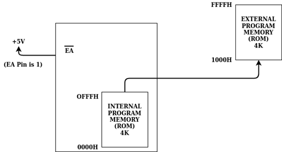
Figure 8. External access
There is also an alternative method to fetch the instructions where the Internal ROM is ignored and instructions are fetched only from External Program Memory (External ROM).
For this purpose, EA pin must be connected to GND. The memory addresses of external ROM will be from 0000H to FFFFH.
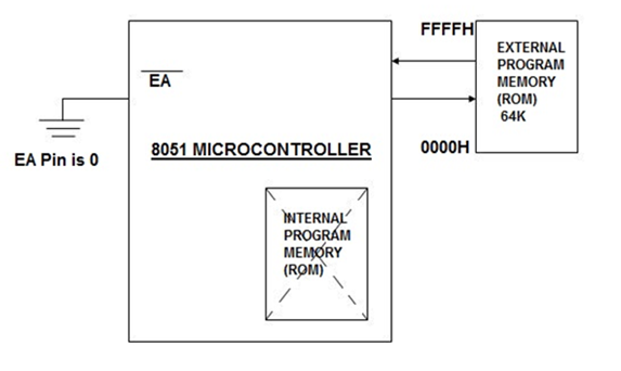
Figure 9. External Program Memory
Q17) With help of block diagram explain all blocks of 8051?
A17)
Block Diagram

Figure 10. Block Diagram of 8051
ALU
ALU performs all arithmetic and logical functions.
Addition, subtraction with carry, and multiplication are categorized as arithmetic operations.
Logical AND, OR and exclusive OR (XOR) as logical operations.
Program Counter (PC)
A program counter is a 16-bit register that has no internal address. The program counter fetches the address of the next instruction to be executed from memory. The PC holds the address of next instruction residing in memory. When a command is encountered, it executes that instruction. PC increments and holds the address of the next instruction.
Registers
Registers are known as data storage devices. There are two registers namely Register A and Register B. Register A is used as an accumulator and Register B as general -purpose register. The output of mathematical and logical instructions are stored in these registers.
The operations of addition, subtraction, multiplication and division are performed by Register A. Register B is for multiplication and division which are carried by Register A. For data transfers between microcontroller and external memory Register A is involved.
8051 microcontrollers also has 7 Special Function Registers (SFRs). They are:
1. Serial Port Data Buffer (SBUF)
2. Timer/Counter Control (TCON)
3. Timer/Counter Mode Control (TMOD)
4. Serial Port Control (SCON)
5. Power Control (PCON)
6. Interrupt Priority (IP)
7. Interrupt Enable Control (IE)
4. Timers and Counters
In internal operations synchronization is achieved by clock circuits for generating clock pulses. During each clock pulse operations assure synchronization.
For oscillator formation XTAL1 and XTAL2 are used to form resonant network. It consists of four more pins.
1. EA: External enable
2. ALE: Address latch enable
3. PSEN: Program store enable and
4. RST: Reset.
Quartz crystal is used for generating periodic clock pulses.
5. Internal RAM and ROM
ROM
In 8051 a code of 4K memory is incorporated as on-chip ROM. ROM is a non-volatile memory that is its contents cannot be altered. They can address program memory and data memory which is a separate block of 64KB.
RAM
The internal RAM of 8051 microcontroller is composed of 128 bytes. It is a volatile memory because its contents is lost if power is switched off.
In internal RAM 128 bytes is divided into 32 working registers which constitute of 4 register banks (Bank 0-Bank 3) , each bank consisting of 8 registers (R0 - R7). Internal RAM consists of 128 addressable bits.

6. Four General Purpose Parallel Input/Output Ports
It consists of four 8-bit input/output ports. These are:
PORT P0: In absence of external memory present, this port acts as a general-purpose input/output port. In the presence of external memory, it operates as multiplexed address and data bus performing dual role.
PORT P1: This port is used for different interfacing activities. This 8-bit port is a normal I/O port and does not perform dual functions.
PORT P2: Port 2 is like PORT P0 which is used as general- purpose port if no external memory is present. However, in presence of external memory, it works in conjunction with PORT PO as an address bus. This is an 8-bit port which performs dual functions.
PORT P3: PORT P3 behaves as dedicated I/O port.
7. Interrupt Control
An interrupt is either an internal or external event where the microcontroller suspends for a certain time by obstructing the sequential flow of a program.
There are two ways of giving interrupts to a microcontroller
- Sending software instructions
- Sending hardware signals.
In interrupt mechanism 8051 keeps the normal program execution in “put on hold" mode and executes a subroutine program. After execution of subroutine it returns to normal program execution. This subroutine program is called an interrupt handler. A subroutine is executed when certain event occurs.
8051 is provided with 5 sources of interrupts are provided. They are:
a) Two external interrupt sources connected through INT0 and INT1
b) Three external interrupt sources- serial port interrupt, Timer Flag 0 and Timer Flag 1.
8. Serial Data Communication
In serial data communication is established among computers by transmitting and receiving data bits in a serial connection network.
For holding data SBUF (Serial Port Data Buffer) register;
Manage data communication SCON (Serial Control) register
Managing data transfer rate PCON (Power Control) register
RXD and TXD establish serial network.
SBUF register has 2 parts
For storing the data to be transmitted use TXD pin
For receiving data from other source use RXD pin.
Serial data communication operate in four modes. They are serial data
1. Mode 0 (shift register mode)
2. Mode 1 (standard UART)
3. Mode 2 (multiprocessor mode)
4. Mode 3
9. PSW (Program Status Word)
Program Status Word or PSW is a hardware register a memory location which holds a program's information and monitors the status of the program this is currently being executed. It has a pointer which points towards the address of the next instruction to be executed.
The register has 3 fields namely instruction address field, condition code field and error status field. PSW is an internal register which keeps track of the computer at every instant.
There are7 flags in PSW. 4 are math flags and 3 are general purpose or user flags.
The Math flags are:
• Carry (c)
• Auxiliary carry (AC)
• Overflow (OV)
• Parity (P)
The General-purpose flags or User flags are:
• FO
• GFO
• GF 1
10. Data Pointer (DPTR)
DPTR is a 16-bit register. It consists of two 8-bit registers DPH and DPL. Separate addresses are assigned to each DPH and DPL. These 8-bit registers are used for storing memory addresses which can be accessed internal and external data/code.
11. Stack Pointer (SP)
A special area of data in memory. The stack pointer is an 8-bit register whose main function is to access the stack. It can take values in the range 00 H to FF H. SP acts as a pointer to points to an address at the top of the stack.
12. Data and Address Bus
A bus consists of group of wires to transfer data from one location to another within the system. Buses reduce the number of paths or cables needed to set up connection between components.
There are two kinds of buses - Data Bus and Address Bus
Data Bus: The purpose of data bus is to transfer data. It acts as a channel for data to travel.
Address Bus: The purpose of address bus is to transfer information but not data. The information tells from where within the components, the data should be sent to or received from.
Q18) Explain features of 32-bit microcontroller?
A18)
Characteristics of 32-bit microcontroller
- This has high performance RISC CPU.
- 40-pin PDIP, high performance, enhanced Flash Microcontroller with CAN.
- The Operating speed ranges between 40 MHz up to 10 MIPS.
- The Operating voltage ranges 4.2 to 5.5 V
- ROM of size 2M bytes
- RAM between 256 bytes to 4096 bytes.
- On-chip program ROM in form of flash memory.
- Data EEPROM
- 8 x 8 Single cycle Hardware Multiplier
- 16-bit wide instructions, 8-bit wide data path.
- 75 instructions.
- ADC and USART PROTOCOL for PC communication.
- I/O port between 16 to 72 pins and I/O port register are bit and port accessible.
- SPI PROTOCOL and I2C PROTOCOL for memory communication.
- PIC 18F458 has two-stage pipeline.
- Interrupt capability with Priority levels.
- Linear program memory addressing upto 2 Mbytes
Unit - 1
Unit - 1
Unit - 1
Introduction to Microcontroller
Q1) Explain the main features of 8-bit microcontroller?
A1)
Characteristics 8-bit microcontroller with an integrated CAN module
1. A 32 k flash program memory,
2. A 1536-byte RAM data memory,
3. A 256-byte EEPROM memory,
4. Twenty two I/O ports,
5. Five-channel 10-bit A/D converters,
6. Three timers/counters,
7. Three external interrupt pins,
8. High current (25-mA) sink/source,
9. Capture/compare/Pulse Width Modulation (PWM) module,
10. SPI/I2C module,
11. CAN 2.0A/B module,
12. Power-on reset and power-on timer,
13. Watchdog timer,
14. Priority level interrupts,
15. DC to 40-MHz clock input,
16. An 8 × 8 hardware multiplier,
17. Wide operating voltage (2.0–5.5 V),
18. Power saving sleep mode.
Q2) Explain features of 16-bit microcontroller?
A2)
CPU16
1. 16 Bit Architecture
2. Control-Oriented Digital Signal Processing Capability
3. 16 bit Multiply and Accumulate (digital signal processing)
4. 1 Megabyte of Program Memory Space and 1 Megabyte of Data Memory Space
5. High Level Language Support
6.Fast Interrupt Response Time
7. Hardware Breakpoint Signal
8. Background Debugging Mode (BDM)
9. Fully Static Operation
10. Watchdog Timer, Clock Monitor and Bus Monitor
11. Parallel Ports Option on Address and Data Bus in Single Chip Mode
12. Two 8 bit Dual Function Input/Output Ports
13. One 7 bit Dual Function Output Port
14. Phase-Locked Loop (PLL) Clock System
15. Multichannel Communication Interface (MCCI)
17. Two channels of enhanced Serial Communication Interface (SCI) (UART)
18. One channel of Serial Peripheral Interface (SPI)
19. Configurable Timer Module Version 7 (CTM7)
20. One 16 bit modulus counters (MCSM)
21. One 16 Bit Free-Running Counter (FCSM)
22. Six single-action submodules (SASM)
Q3) Explain the architecture of 8051 microcontroller?
A3)
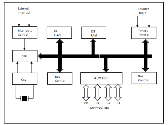
Figure 1. 8051 Architecture
Central Processor Unit (CPU)
The brain of any processing device of the microcontroller is the CPU. It monitors and controls all operations performed on these units. It reads program written in ROM memory, executes and does the expected task.
Interrupts
Interrupt is a subroutine call that interrupts the microcontrollers main operations or work and causes it to execute any other program, at the time of operation. It provides a mechanism to put on hold the ongoing operations, execute a subroutine and resume to another type of operation.
8051 has five interrupt sources:
INTO
TFO
INT1
TF1
R1/T1
(INT0) ̅ and (INT1) ̅ are external interrupts negative edge triggered or low level triggered. When these interrupts are activated, the corresponding flags are set except for serial interrupt.
When the processor branches to ISR the interrupt flags are cleared. The external interrupts are timer and serial port interrupts.
Memory
They require memory to save as well as read so that the microcontroller performs specific operations of the task.
The memory which is used to store the program known as code memory or Program memory It is also known as ROM memory.
8051 data memory is used to storing data temporarily for operation known as RAM memory. It has 4K of code memory or program memory and 128 bytes of data memory of RAM.
BUS
A collection of wires that work as communication channel or medium for transfer of data. It consists of 8, 16 or more wires of microcontroller. Thus, they carry 8 bits or 16 bits of data simultaneously. There are two types of buses which are
Address Bus
Data Bus
Address Bus:
Microcontroller 8051 has a 16-bit address bus for transferring data. It addresses memory locations to transfer address from CPU to Memory. It has four addressing modes that are:
Immediate addressing modes.
Bank address (or) Register addressing mode.
Direct Addressing mode.
Register indirect addressing mode.
Data Bus: Microcontroller 8051 has 8 bits of data bus used to carry data for applications.
Oscillator
The 8051 microcontroller has an on-chip oscillator that acts as a clock source for CPU of microcontroller. The output pulses of the oscillator are stable. Therefore, it enables synchronized work for all the parts of Microcontroller system.
Input/output Port
To control the operation of machines microcontroller is used in embedded systems. To connect to other machines, devices or peripherals I/O interfacing ports is required. Microcontroller 8051 has 4 input and output ports to connect to other peripherals
Timers/Counters
8051 microcontroller has two 16-bit timers and counters. The counters are again divided into 8-bit register. Timers are used for measurement of time intervals to determine pulse width.
Q4) What are Special function registers, explain SRF map?
A4)
Registers are known as data storage devices. There are two registers namely Register A and Register B. Register A is used as an accumulator and Register B as general -purpose register. The output of mathematical and logical instructions is stored in these registers.
The operations of addition, subtraction, multiplication and division are performed by Register A. Register B is for multiplication and division which are carried by Register A. For data transfers between microcontroller and external memory Register A is involved.
8051 microcontrollers also has 7 Special Function Registers (SFRs). They are:
1. Serial Port Data Buffer (SBUF)
2. Timer/Counter Control (TCON)
3. Timer/Counter Mode Control (TMOD)
4. Serial Port Control (SCON)
5. Power Control (PCON)
6. Interrupt Priority (IP)
7. Interrupt Enable Control (IE)
Internal Data Memory and Special Function Register (SFR) Map
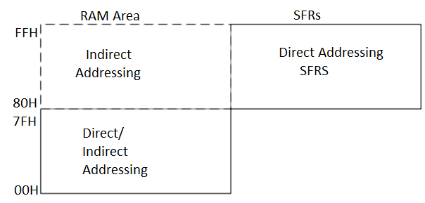
The special function registers (SFRs) are mapped in the upper 128 bytes of internal data memory address. Hence there is an address overlap between the upper 128 bytes of data RAM and SFRs. Please note that the upper 128 bytes of data RAM are present only in the 8052 family. The lower128 bytes of RAM (00H - 7FH) can be accessed both by direct or indirect addressing while the upper 128 bytes of RAM (80H - FFH) are accessed by indirect addressing. The SFRs (80H - FFH) are accessed by direct addressing only. This feature distinguishes the upper 128 bytes of memory from the SFRs, as shown in figure above.
SFR Map
The set of Special Function Registers (SFRs) contains important registers such as Accumulator, Register B, I/O Port latch registers, Stack pointer, Data Pointer, Processor Status Word (PSW) and various control registers. Some of these registers are bit addressable (they are marked with a * in the diagram below). The detailed map of various registers is shown in the following figure.

Q5) Explain the PCON and SCON register with all its bits?
A5)
Peripheral Control Registers PCON (Power Control)
The PCON or Power Control register, as the name suggests is used to control the 8051 Microcontroller’s Power Modes and is located at 87H of the SFR Memory Space. Using two bits in the PCON Register, the microcontroller can be set to Idle Mode and Power Down Mode. During Idle Mode, the Microcontroller will stop the Clock Signal to the ALU (CPU) but it is given to other peripherals like Timer, Serial, Interrupts, etc. In order to terminate the Idle Mode, you have to use an Interrupt or Hardware Reset. In the Power Down Mode, the oscillator will be stopped and the power will be reduced to 2V. To terminate the Power Down Mode, you have to use the Hardware Reset. Apart from these two, the PCON Register can also be used for few additional purposes. The SMOD Bit in the PCON Register is used to control the Baud Rate of the Serial Port. There are two general purpose Flag Bits in the PCON Register, which can be used by the programmer during execution.
SCON (Serial Control)
The Serial Control or SCON SFR is used to control the 8051 Microcontroller’s Serial Port. It is located as an address of 98H. Using SCON, you can control the Operation Modes of the Serial Port, Baud Rate of the Serial Port and Send or Receive Data using Serial Port. SCON Register also consists of bits that are automatically SET when a byte of data is transmitted or received.

Q6) Explain TMOD and TCON registers?
A6)
TCON (Timer Control)
Timer Control or TCON Register is used to start or stop the Timers of 8051 Microcontroller. It also contains bits to indicate if the Timers has overflowed. The TCON SFR also consists of Interrupt related bits.

TMOD (Timer Mode)
The TMOD or Timer Mode register or SFR is used to set the Operating Modes of the Timers T0 and T1. The lower four bits are used to configure Timer0 and the higher four bits are used to configure Timer1.
Q7) What is IP register explain all its bits?
A7)
IP (Interrupt Priority)
The IP or Interrupt Priority Register is used to set the priority of the interrupt as High or Low. If a bit is CLEARED, the corresponding interrupt is assigned low priority and if the bit is SET, the interrupt is assigned high priority.
Peripheral Data Registers SBUF (Serial Data Buffer)
The Serial Buffer or SBUF register is used to hold the serial data while transmission or reception.
Q8) What is the clock frequency of 8051? Explain the clock and reset circuit?
A8)
RESET is an active High input when RESET is set to High, 8051 goes back to the power on state. 8051 is reset by holding the RST high for at least two machine cycles and then returning it low.
There are two methods of reset circuit:
1.Power On Reset.
- Initially charging of capacitor makes RST High
- When capacitor charges fully it blocks DC.
2.Manual Reset
- Closing the switch momentarily will make RST High.
After a reset, the program counter is loaded with 0000H but the content of on-chip RAM is not affected.
Clock Circuit
- The 8051 uses the crystal for precisely that to synchronize it’s operation. Effectively, the 8051 operates using what are called "machine cycles."
- A single machine cycle is the minimum amount of time in which a single 8051 instruction can be executed. Although many instructions take multiple cycles.
- 8051 has an on-chip oscillator. It needs an external crystal that decides the operating frequency of the 8051.

- The crystal is connected to pins 18 and 19 with stabilizing capacitors. 12 MHz (11.059MHz) crystal is often used and the capacitance ranges from 20pF to 40pF.
- The oscillator can also be a TTL clock source connected with a NOT gate as shown.
Q9) Explain the register banks of 8051 along with memory locations?
A9)
A total of 32 bytes of RAM are set aside for the register banks and stack. These 32 bytes are divided into 4 banks of registers in which each bank has 8 registers, RO - R7. RAM locations from 0 to 7 are set aside for bank 0 after RO - R7 where RO is RAM location 0, RI is RAM location I, R2 is location 2, and so on, until memory location 7, which belongs to R7 of bank O. The second bank of registers RO - R7 starts at RAM location 08 and goes to location OFH. The third bank of RO - R7 starts at memory location 10H and goes to location
17H. Finally, RAM locations 18H to 1FH arc set aside for the fourth bank of RO- R7. The following shows how the 32 bytes are allocated into 4 banks

As we see from above the bank uses the same RAM space as the stack. This IS a major problem in programming the 8051. We must either not use register bank I, or allocate another area of RAM for the stack.
Q10) Explain the concept of stack in 8051?
A10)
The stack is a section of RAM used by the CPU to store information temporarily. This information could be data or an address. The CPU needs this storage area since there are only a limited number of registers.
If the stack is a section of RAM, there must be registers inside the CPU to point to it. The register used to access the stack is called the SP (stack pointer) register. The stack pointer in the 8051 is only 8 bits wide, which means that It can take values of 00 to FFH. When the 8051 is powered up, the SP register contains value 07. This means that RAM location 08 is the first location used for the stack by the 8051. The storing of a CPU register in the stack is called a PUSH, and pulling the contents off the stack back into a CPU register is called a POP. In other words, a register is pushed onto the stack to save it and popped off the stack to retrieve it. The job of the SP is very critical when push and pop actions arc performed. To see how the stack works, let's look at the PUSH and POP instructions.
Q11) Explain the effect of PUSH instruction on stack?
A11)
In the 8051 the stack pointer (SP) points to the last used location of the stack. As we push data onto the stack, the stack pointer (SP) is incremented by one. Notice that this is different from many microprocessors, notably x86 processors in which the SP is decremented when data is pushed onto the stack. Examining Example, we see that as each PUSH is executed, the contents of the register arc saved on the stack and SP is incremented by I. Notice that for every byte of data saved on the stack, SP IS incremented only once. Notice also that to push the registers onto the stack we must use their RAM addresses. For example the instruction "PUSH1" pushes register R1 onto the stack
Show the stack and stack pointer for the following. Assume the default stack area and register 0 is selected.
MOV R6,#25H
MOV Rl,#12H
MOV R4,#OF3H
PUSH 6
PUSH 1
PUSH 4

Q12) Explain the execution of CALL instruction with help of any program?
A12)
In addition to using the stack to save registers, the CPU also uses the stack to save the address of the instruction just below the CALL instruction. This is how the CPU knows where to resume when it returns from the called subroutine.
Show the stack and stack pointer for the following instructions,
MOV SP, #5FH; make RAM location 60H
MOV R2, #25H; first stack location
MOV Rl, #12H
MOV R4, #OF3H
PUSH 2
PUSH 1
PUSH 4
Q13) What is Program Counter? Explain step by step execution of a program byte by byte?
A13)
Another important register in the 8051 is the PC (program counter). The program counter points to the address of the next instruction to be executed. As the CPU fetches the opcode from the program ROM, the program counter is incremented to point to the next instruction. The program counter in the 8051 is 16 bits wide. This means that the 8051 can access program addresses 0000 to FFFFH, a total of 64K bytes of code. However, not all members of the 8051 have the entire 64K bytes of on-chip ROM installed.
Program Counter (PC) – 16 bit PC contains the address of next instruction to be executed. On reset PC will set to 0000. After fetching every instruction PC will increment by one.
When the 8051 is powered up, the PC (program counter) has the value of 0000 in it. This means that it expects the first opcode to be stored at ROM address OOOOH. For this reason, in the 8051 system, the first opcode must be burned into memory location OOOOH of program ROM since this is where it looks for the first instruction when it is booted. We achieve. This by the ORG statement in the source program as shown earlier.
Executing a program byte by byte
Assuming that the above program is burned into the ROM of an 8051 chip (or 8751, AT895I, or DS5000), the following is a step-by-step description of the action of the 8051 upon applying power to it.
I. When the 8051 is powered up, the PC (program counter) has 0000 and starts to fetch the first opcode from location 0000 of the program ROM. In the case of the above program the first opeode is 70, which is the code for moving an operand to R5. Upon executing the opcode, the CPU fetches the value 25 and places it in R5. Now once instruction is finished. Then the program counter is incremented to point to 0002 (PC = 0002), which contains opcode 7F, the opcode for the instruction "MOV R7".
2. Upon executing the opcode 7F, the value 34H is moved into R7. Then the program counter is incremented to 0004.
3. ROM location 0004 has the opcode for the instruction "MOV A, #0". This instruction is executed and now PC = 0006. Notice that all the above instructions arc 2-byte instructions; that is, each one takes two memory locations.
4. Now PC = 0006 points to the next instruction, which is "ADD A, RS". This is a l-byte instruction. After the execution of this instruction, PC = 0007.
5. The location 0007 has the opcode 2F, which belongs to the instruction "ADD A, R7". This also is a l-byte instruction. Upon execution of this instruction PC is incremented to 0008. This process goes on until all the instructions are fetched. And executed. The fact that the program counter points at the next instruction to be executed explains why some microprocessors (notably the x86) call the program counter the ins/ruction pointer.
Q14) Explain port structure of 8051?
A14)
Port Structure
8051 has four ports P0, P1, P2, P3. They are required for I/O operations.
32 pins are set for four ports P0,P1,P2,P3. Each port takes 8 pins.
All the ports are configured as input upon Reset
When zero is written to port it becomes output. To make it input 1 needs to be sent to the port.
Port 0:

Fig 2. Port -0
When Port0 is used as input port 1 must be written to the corresponding zero latch that causes the output transistor to switch off and pin floats in high impedance state.
When configured as input port it provides two facilities:
Reads logic level on physical pin by asserting read pin signal.
Read contents of internal latch by asserting the read latch signal.
The latch is read for instruction read-modify-write type instruction.
It reads data from the port modifies and writes to the port.
When Port0 is configured as output the latch pins that are programmed to 0 will cause the lower FET to turn ON and pin is grounded.
If 1 is written to the latch pin FET will turn OFF and pin is pulled HIGH by external pull-up resistor.
Port 1:

Figure 3. Port 1 circuit
When port 1 is used as in input port ‘1’ must be written to the corresponding port1 latch bit. This causes the lower FET to turn off.
The pin and the input buffer are pulled to logic HIGH by internal pull load.
This port is called quasi-bidirectional port because its output is pulled high with pull up resistor.
When port 1 is used as an output port, the latch pins that are programmed to 0, will cause the lower FET turn on the internal pull to turn off and input is logic 0.
If 1 is written onto the latch, then it will drive the input of external circuit high through pull up. The lower FET turns off.
Port 2:
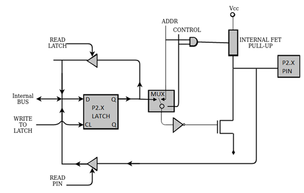
Figure 4. Port 2 circuit
When Port2 is used as an input port 1 must be written to the corresponding latch bit. This cause the FET turn off. The pin and input to pin buffer are pulled to logic high by internal pull up load.
Port 2 is called as “quasi-bidirectional port” as its output is pull up resistors.
When port2 is used as output port the latch pins that are programmed to 0, will cause the lower FET to turn off and input to the circuit logic 0.
If “1” is written onto latch pin, then it will drive the input of external circuit high through pull-up. The lower FET turns off.
Port 3:
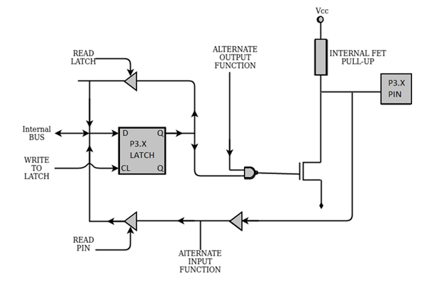
Figure 5. Port 3 circuit
When port3 is used as input port 1 must be written to the corresponding port3 latch bit.
This causes FET to turn off.
The pin and input to the buffer are pulled to logic HIGH by internal pull up load.
When port3 is used as output port, the latched pins that are programmed to 0 will cause to lower FET to turn on and internal pull up to turn off and input to circuit is logic 0.
If 1 is written onto latch pin it will drive the input external circuit high through pull up. The lower FET turns off.
Q15) Explain the Data memory of 8051 microcontroller?
A15)
Data Memory or RAM stores temporary data and intermediate results generated during the normal operation of the microcontroller.
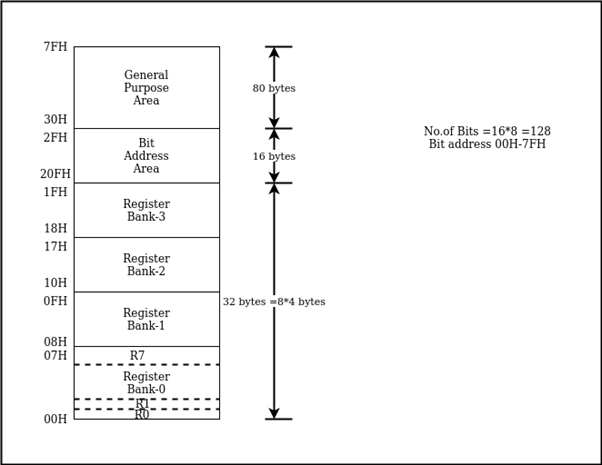
Currently, 8051 Microcontroller has 256B of RAM. The first 128B memory addresses from 00H to 7FH is divided in to Working Registers. They are organized as Register Banks, Bit – Addressable Area and General-Purpose RAM known as Scratchpad area.
The first 128B of RAM (from 00H to 7FH), the first 32B of memory from addresses 00H to 1FH consists of 32 Working Registers organized into four banks with 8 Registers in each Bank.
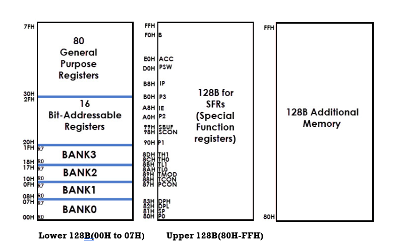
Fig 6. (Direct and Indirect Addressing) (Direct Addressing) (Indirect Addressing)
The 4 banks are named as Bank0, Bank1, Bank2 and Bank3. Each Bank consists of 8 registers R0 – R7. Each Register can be addressed either by name or by address.
To address the register by name, first the corresponding bank is selected. In order to select the bank, RS0 and RS1 bits of the Program Status Word (PSW) and Register (RS0 and RS1 are 3rd and 4th bits in the PSW Register) are used.
When addressing these Register for example 12H the corresponding bank may or may not be selected. (12H corresponds to R2 in Bank2).
The next 16B of the RAM that is from 20H to 2FH are Bit – Addressable memory locations. A total of 128 bits can be addressed individually using 00H to 7FH or an entire byte can be addressed as 20H to 2FH.
The final 80B of the internal RAM addresses are from 30H to 7FH which is the general-purpose RAM area are byte addressable.
These lower 128B of RAM can be addressed directly or indirectly.
Q16) Explain the ROM (Program Memory) of 8051?
A16)
The code or instructions which are to be executed are stored in the Program Memory, also called as the ROM of the Microcontroller.
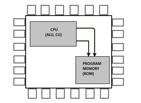
Figure 7. Program Memory
In 4KB Internal ROM, the address space is 0000H to 0FFFH. If the program addresses exceed this value, CPU will automatically fetch the code from the external Program Memory.
For External Access (EA Pin) must be pulled HIGH at this condition the CPU first fetches instructions from the Internal Program Memory in the address range of 0000H to 0FFFFH. If it exceeds the memory addresses limit, instructions are fetched from external ROM in address range of 1000H to FFFFH.

Figure 8. External access
There is also an alternative method to fetch the instructions where the Internal ROM is ignored and instructions are fetched only from External Program Memory (External ROM).
For this purpose, EA pin must be connected to GND. The memory addresses of external ROM will be from 0000H to FFFFH.

Figure 9. External Program Memory
Q17) With help of block diagram explain all blocks of 8051?
A17)
Block Diagram
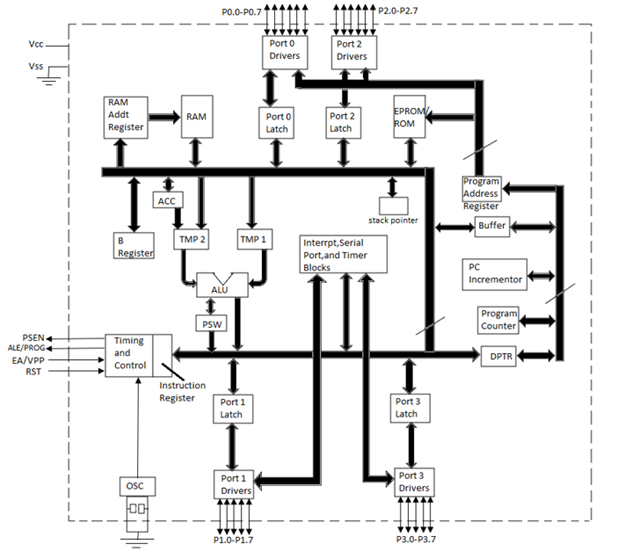
Figure 10. Block Diagram of 8051
ALU
ALU performs all arithmetic and logical functions.
Addition, subtraction with carry, and multiplication are categorized as arithmetic operations.
Logical AND, OR and exclusive OR (XOR) as logical operations.
Program Counter (PC)
A program counter is a 16-bit register that has no internal address. The program counter fetches the address of the next instruction to be executed from memory. The PC holds the address of next instruction residing in memory. When a command is encountered, it executes that instruction. PC increments and holds the address of the next instruction.
Registers
Registers are known as data storage devices. There are two registers namely Register A and Register B. Register A is used as an accumulator and Register B as general -purpose register. The output of mathematical and logical instructions are stored in these registers.
The operations of addition, subtraction, multiplication and division are performed by Register A. Register B is for multiplication and division which are carried by Register A. For data transfers between microcontroller and external memory Register A is involved.
8051 microcontrollers also has 7 Special Function Registers (SFRs). They are:
1. Serial Port Data Buffer (SBUF)
2. Timer/Counter Control (TCON)
3. Timer/Counter Mode Control (TMOD)
4. Serial Port Control (SCON)
5. Power Control (PCON)
6. Interrupt Priority (IP)
7. Interrupt Enable Control (IE)
4. Timers and Counters
In internal operations synchronization is achieved by clock circuits for generating clock pulses. During each clock pulse operations assure synchronization.
For oscillator formation XTAL1 and XTAL2 are used to form resonant network. It consists of four more pins.
1. EA: External enable
2. ALE: Address latch enable
3. PSEN: Program store enable and
4. RST: Reset.
Quartz crystal is used for generating periodic clock pulses.
5. Internal RAM and ROM
ROM
In 8051 a code of 4K memory is incorporated as on-chip ROM. ROM is a non-volatile memory that is its contents cannot be altered. They can address program memory and data memory which is a separate block of 64KB.
RAM
The internal RAM of 8051 microcontroller is composed of 128 bytes. It is a volatile memory because its contents is lost if power is switched off.
In internal RAM 128 bytes is divided into 32 working registers which constitute of 4 register banks (Bank 0-Bank 3) , each bank consisting of 8 registers (R0 - R7). Internal RAM consists of 128 addressable bits.
6. Four General Purpose Parallel Input/Output Ports
It consists of four 8-bit input/output ports. These are:
PORT P0: In absence of external memory present, this port acts as a general-purpose input/output port. In the presence of external memory, it operates as multiplexed address and data bus performing dual role.
PORT P1: This port is used for different interfacing activities. This 8-bit port is a normal I/O port and does not perform dual functions.
PORT P2: Port 2 is like PORT P0 which is used as general- purpose port if no external memory is present. However, in presence of external memory, it works in conjunction with PORT PO as an address bus. This is an 8-bit port which performs dual functions.
PORT P3: PORT P3 behaves as dedicated I/O port.
7. Interrupt Control
An interrupt is either an internal or external event where the microcontroller suspends for a certain time by obstructing the sequential flow of a program.
There are two ways of giving interrupts to a microcontroller
- Sending software instructions
- Sending hardware signals.
In interrupt mechanism 8051 keeps the normal program execution in “put on hold" mode and executes a subroutine program. After execution of subroutine it returns to normal program execution. This subroutine program is called an interrupt handler. A subroutine is executed when certain event occurs.
8051 is provided with 5 sources of interrupts are provided. They are:
a) Two external interrupt sources connected through INT0 and INT1
b) Three external interrupt sources- serial port interrupt, Timer Flag 0 and Timer Flag 1.
8. Serial Data Communication
In serial data communication is established among computers by transmitting and receiving data bits in a serial connection network.
For holding data SBUF (Serial Port Data Buffer) register;
Manage data communication SCON (Serial Control) register
Managing data transfer rate PCON (Power Control) register
RXD and TXD establish serial network.
SBUF register has 2 parts
For storing the data to be transmitted use TXD pin
For receiving data from other source use RXD pin.
Serial data communication operate in four modes. They are serial data
1. Mode 0 (shift register mode)
2. Mode 1 (standard UART)
3. Mode 2 (multiprocessor mode)
4. Mode 3
9. PSW (Program Status Word)
Program Status Word or PSW is a hardware register a memory location which holds a program's information and monitors the status of the program this is currently being executed. It has a pointer which points towards the address of the next instruction to be executed.
The register has 3 fields namely instruction address field, condition code field and error status field. PSW is an internal register which keeps track of the computer at every instant.
There are7 flags in PSW. 4 are math flags and 3 are general purpose or user flags.
The Math flags are:
• Carry (c)
• Auxiliary carry (AC)
• Overflow (OV)
• Parity (P)
The General-purpose flags or User flags are:
• FO
• GFO
• GF 1
10. Data Pointer (DPTR)
DPTR is a 16-bit register. It consists of two 8-bit registers DPH and DPL. Separate addresses are assigned to each DPH and DPL. These 8-bit registers are used for storing memory addresses which can be accessed internal and external data/code.
11. Stack Pointer (SP)
A special area of data in memory. The stack pointer is an 8-bit register whose main function is to access the stack. It can take values in the range 00 H to FF H. SP acts as a pointer to points to an address at the top of the stack.
12. Data and Address Bus
A bus consists of group of wires to transfer data from one location to another within the system. Buses reduce the number of paths or cables needed to set up connection between components.
There are two kinds of buses - Data Bus and Address Bus
Data Bus: The purpose of data bus is to transfer data. It acts as a channel for data to travel.
Address Bus: The purpose of address bus is to transfer information but not data. The information tells from where within the components, the data should be sent to or received from.
Q18) Explain features of 32-bit microcontroller?
A18)
Characteristics of 32-bit microcontroller
- This has high performance RISC CPU.
- 40-pin PDIP, high performance, enhanced Flash Microcontroller with CAN.
- The Operating speed ranges between 40 MHz up to 10 MIPS.
- The Operating voltage ranges 4.2 to 5.5 V
- ROM of size 2M bytes
- RAM between 256 bytes to 4096 bytes.
- On-chip program ROM in form of flash memory.
- Data EEPROM
- 8 x 8 Single cycle Hardware Multiplier
- 16-bit wide instructions, 8-bit wide data path.
- 75 instructions.
- ADC and USART PROTOCOL for PC communication.
- I/O port between 16 to 72 pins and I/O port register are bit and port accessible.
- SPI PROTOCOL and I2C PROTOCOL for memory communication.
- PIC 18F458 has two-stage pipeline.
- Interrupt capability with Priority levels.
- Linear program memory addressing upto 2 Mbytes