Unit - 4
A/D and D/A Converters
Q1) Explain weighted resistor A/D converter.
A1)
In the weighted resistor type DAC, each digital level is converted into an equivalent analog voltage or current.
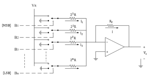
The following figure is the binary weighted resistor type DAC.
Here 
It consists of parallel binary weighted resistor bank and a feedback resistor Rf.
The switch positions decide the binary word (i.e.B1B2B3…Bn).
Here, op-amp is used as current to voltage converter.
Disadvantages:
1) When number of binary input increases, it is not easy to maintain the resistance ratio.
2) Very wide ranges of different values of resistors are required.
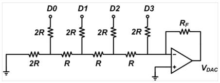
Q2) Find the output voltage of R-2R ladder D/A Converter.
A2)
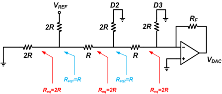
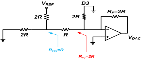
Circuit Operation
Assume that D0 is connected to VREF and the other bits are logic low
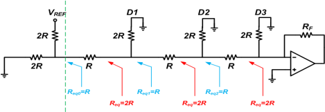
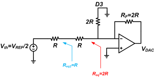
Applying the Thevenin theorem

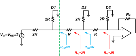

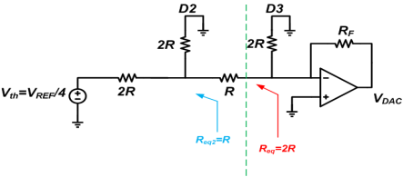
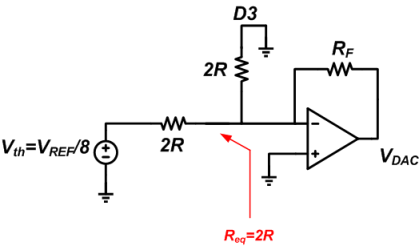
Assuming RF=2R, the output voltage will be VDAC = -2R ✖ (VREF/8)/2R = -VREF/8.
This output voltage corresponds to the DAC LSB.
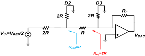
This is the same as Figure except that the input is VREF/2 instead of VREF/4. Considering the result of the case D3D2D1D0 = 0001, if RF = 2R we obtain VDAC = -VREF/4.
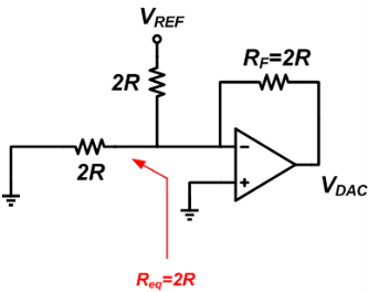
The output voltage will be VDAC = -(VREF/2R)✕2R = -VREF.
Q3) Explain Sample and Hold Circuit with suitable diagram.
A3)
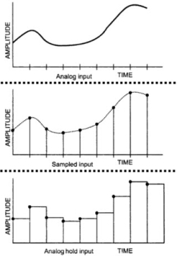
A Sample and Hold Circuit, sometimes represented as S/H Circuit or S & H Circuit, is usually used with an Analog to Digital Converter to sample the input analog signal and hold the sampled signal.
In the S/H Circuit, the analog signal is sampled for a short interval of time, usually in the range of 10µS to 1µS. After this, the sampled value is hold until the arrival of next input signal to be sampled. The duration for holding the sample will be usually between few milliseconds to few seconds.
The following image shows a simple block diagram of a typical Sample and Hold Circuit.
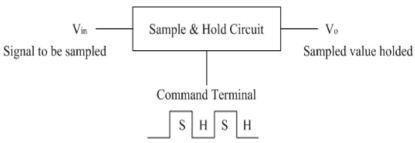
This sample and hold circuit consist of two basic components:
- Analog Switch
- Holding Capacitor
The following image shows the basic S/H Circuit.

This circuit tracks the input analog signal until the sample command is changed to hold command. After the hold command, the capacitor holds the analog voltage during the analog to digital conversion.
The following image shows the input and output of a typical Sample and Hold Circuit.
Q4) What is an Analog Switch? Explain its types.
A4)
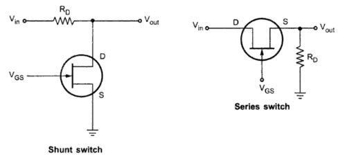
Any FET like JFET or MOSFET can be used as an Analog Switch. In this discussion, we will concentrate on JFET. The Gate-Source voltage VGS is responsible for switching the JFET.
When VGS is equal to 0V, the JFET acts as a closed switch as it operates in its Ohmic region. When VGS is a large negative voltage (i.e. more negative than VGS(OFF)), the JFET acts as an open switch as it is cut-off.
The switch can be either a Shunt Switch or a Series Switch, depending on its position with respect to input and output. The following image shows a JFET configured as both a Shunt Switch and as a Series Switch.
Q5) Explain successive approximation A to D converter with suitable example.
A5)
- Successive Approximation type ADC is the most widely used and popular ADC method.
- The conversion time is maintained constant in successive approximation type ADC, and is proportional to the number of bits in the digital output, unlike the counter1and continuous type A/D converters.
- The basic principle is that the unknown analog input voltage is approximated against an n-bit digital value by trying one bit at a time, starting with the MSB.
- It operates by successively dividing the voltage range by half.
(1) The MSB is initially set to 1 with the remaining three bits set as 000. The digital equivalent voltage is compared with the unknown analog input voltage.
(2) If the analog input voltage is higher than the digital equivalent voltage, the MSB is retained as 1 and the second MSB is set to 1
Example:
Let us assume that the 4-bit ADC is used and the analog input voltage is VA = 10V. When the conversion starts, the MSB bit is set to 1.
Now VA = 10V > VD = 8V = [1000]2
Since the unknown analog input voltage VA is higher than the equivalent digital voltage VD, as discussed in step (2), the MSB is retained as 1 and the next MSB bit is set to 1 as follows
VD = 12V = [1100]2
Now VA = 11V < VD = 12V = [1100]2
Here now, the unknown analog input voltage VA is lower than the equivalent digital voltage VD. As discussed in step (2), the second MSB is set to 0 and next MSB set to 1 as
VD = 10V = [1010]2
Now again VA = 9V > VD = 9V = [1001]2
Again as discussed in step (2) VA>VD, hence the third MSB is retained to 1 and the last bit is set to 1.
The new code word is
VD = 10V = [1010]2
Now finally VA = VD , and the conversion stops.
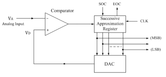
It consists of a successive approximation register (SAR), DAC and comparator. The output of SAR is given to n-bit DAC. The equivalent analog output voltage of DAC, VD is applied to the non-inverting input of the comparator. The second input to the comparator is the unknown analog input voltage VA. The output of the comparator is used to activate the successive approximation logic of SAR.
When the start command is applied, the SAR sets the MSB to logic 1 and other bits are made logic 0, so that the trial code becomes 1000.
Q6) Write the operation and working of Counting A/D Converter.
A6)
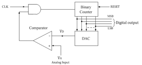
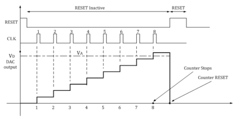
The counter type ADC is made using a binary counter, DAC and a comparator. The output voltage of a DAC is equivalent to corresponding digital input to DAC.
Operation:
- The n-bit binary counter is initially set to 0 by using reset command.
- Therefore the digital output is zero and the equivalent voltage is also 0V.
- When the reset command is removed, the clock pulses go through AND gate and are counted with the binary counter.
- DAC converts the digital output to an analog voltage and applies as an inverting input to the comparator.
- The output enables the AND gate to pass the clock.
- The number of clock pulses increases with the increase in time and the analog input voltage is a rising staircase waveform.
- The counting continues until the DAC output equals and just rises more than unknown analog input voltage.
- Then the comparator output becomes low and this disables the AND gate from passing the clock.
- The counting stops when VA< VD.
Q7) Write the operation and working of dual slope type ADC.
A7)
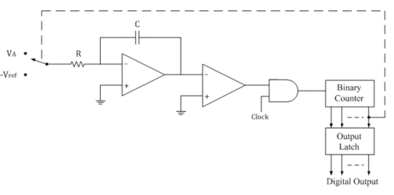
In dual slope type ADC, the integrator generates two different ramps, one with the known analog input voltage VA and another with a known reference voltage –Vref. Hence it is called a s dual slope A to D converter. The logic diagram for the same is shown below.
Operation:
The binary counter is initially reset to 0000; the output of integrator reset to 0V and the input to the ramp generator or integrator is switched to the unknown analog input voltage VA.
The analog input voltage VA is integrated by the inverting integrator and generates a negative ramp output. The output of comparator is positive and the clock is passed through the AND gate. This results in counting up of the binary counter.
The negative ramp continues for a fixed time period t1, which is determined by a count detector for the time period t1. At the end of the fixed time period t1, the ramp output of integrator is given by
∴VS=-VA/RC×t1
When the counter reaches the fixed count at time period t1, the binary counter resets to 0000 and switches the integrator input to a negative reference voltage –Vref.
Now the ramp generator starts with the initial value –Vs and increases in positive direction until it reaches 0V and the counter gets advanced. When Vs reaches 0V, comparator output becomes negative (i.e. logic 0) and the AND gate is deactivated. Hence no further clock is applied through AND gate. Now, the conversion cycle is said to be completed and the positive ramp voltage is given by
∴VS=Vref/RC×t2
Where Vref & RC are constants and time period t2 is variable.
The dual ramp output waveform is shown below.
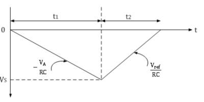
Since ramp generator voltage starts at 0V, decreasing down to –Vs and then increasing up to 0V, the amplitude of negative and positive ramp voltages can be equated as follows.
∴Vref/RC×t2=-VA/RC×t1
∴t2=-t1×VA/Vref
∴VA=-Vref×t1/t2
Thus the unknown analog input voltage VA is proportional to the time period t2, because Vref is a known reference voltage and t1 is the predetermined time period.
The actual conversion of analog voltage VA into a digital count occurs during time t2. The binary counter gives corresponding digital value for time period t2. The clock is connected to the counter at the beginning of t2 and is disconnected at the end of t2.
Thus the counter counts digital output as
Digital Output=(counts/sec) t2
∴Digital output=(counts/sec)[t1×VA/Vref ]
For example, consider the clock frequency is 1 MHz, the reference voltage is -1V, the fixed time period t1 is 1ms and the RC time constant is also 1 ms. Assuming the unknown analog input voltage amplitude as VA = 5V, during the fixed time period t1, the integrator output Vs is
∴VS=-VA/RC×t1=(-5)/1ms×1ms=-5V
During the time period t2, ramp generator will integrate all the way back to 0V.
∴t2=VS/Vref ×RC=(-5)/(-1)×1ms=5ms=5000μs
Hence the 4-bit counter value is 5000, and by activating the decimal point of MSD seven segment displays, the display can directly read as 5V.
Q8) Explain voltage to frequency time conversion.
A8)
Since an analog to digital converter ends up producing a number, wouldn't it be convenient if we could simply count something and have that something proportional to the potential being measured? A voltage to frequency converter ADC does just that. A voltage is integrated until it reaches some pre-set threshold, at which point a comparator trips, doing 2 things:
1) Short circuit the capacitor, resetting the integrator to zero.
2) Produce a pulse that is counted.
Here' the circuit.
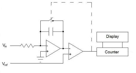
V to F converters integrate noise, and so are useful under circumstances similar to dual slope units. V to F ADCs are precise, accurate, simple, and inexpensive. The precision is directly proportional to the time over which counting occurs, and inversely proportional to the time required to integrate a single count.
If we count pulses for a fixed period of time, then we know how often the comparator tripped during that time. Suppose we want to display 1.000 for a 1 V input, and suppose we look at the input for 1.000 s. Then we'd want the comparator to trip 1000 times per second. Further, suppose the comparator is set up to trip at a potential of 5 V (chosen just so it's not the same as the input potential; in fact, this potential can be anything we like as long as we know it in advance). Then a 1 V input should integrate to 5 V in 1 ms. In the dual slope module, we explained how integrators work. From the argument there, the RC time constant of the integrator is set by Vout = - VinT/(RC).
Ignoring sign, 5 V = 1 V * 1 ms/RC.
RC = 1 ms/5 = 200 μs. For R = 1 kΩ, C = 0.2 μF. Changing the expected magnitude of the input voltage or the number of significant figures desired may mean a different integration time, R, or C value, but for a wide range of inputs the integrate, short, count, repeat cycle works well. The first very high resolution (up to 6 digits or ~ 20 bits) ADCs worked on this principle.
The non-idealities of a V to F converter are dependent on the design strategy. Let's start the simplest approach. Here, we do nothing to compensate for the time required to fully discharge the capacitor; the time while the capacitor is discharging called "dead time." The bigger the resistance of the switch used to short the capacitor, the longer the switch must be closed. Alternatively, if the switch isn't closed for long enough, there will be residual potential on the integrator, and the time to integrate to threshold will be reduced. In practice, if one knows how long the switch is closed, one knows how long the dead time is, and a correction factor may be computed.
Q9) Define Resolution and Accuracy of ADC.
A9)
Resolution
The resolution of the converter indicates the number of discrete values it can produce. It is usually expressed in bits. For example, an ADC that encodes an analogue input to one of 256 discrete values has a resolution of eight bits, since
28 = 256.
Resolution can also be defined electrically, and expressed in volts. The voltage resolution of an ADC is equal to its overall voltage measurement range divided by the number of discrete values.
Accuracy
Accuracy depends on the error in the conversion. If the ADC is not broken, this error has two components: quantization error and (assuming the ADC is intended to be linear) non-linearity. These errors are measured in a unit called the LSB, which is an abbreviation for least significant bit. In the above example of an eight-bit ADC, an error of one LSB is 1/256 of the full signal range, or about 0.4%.
Q10) If Full scale measurement range = 0 to 10 volts then find ADC voltage resolution for 12 bit ADC.
A10)
ADC resolution is 12 bits: 212 = 4096 quantization levels
ADC voltage resolution is: (10-0)/4096 = 0.00244 volts = 2.44 mV
Q11) If Full scale measurement range = -10 to +10 volts then find ADC voltage resolution for 14 bit ADC.
A11)
ADC resolution is 14 bits: 214 = 16384 quantization levels
ADC voltage resolution is: (10-(-10))/16384 = 20/16384 = 0.00122 volts = 1.22 mV