UNIT 4
Question bank
Q1)What do you understand by a semi-conductor? Discuss some important properties of semiconductor
Answer:
A semiconductor is a substance which has resistivity (10−4 to 0.5 Ωm) in-between conductors and insulators e.g. Germanium, silicon, selenium, carbon etc.
Nichrome, which is one of the highest resistance materials, has resistivity much lower than germanium. This shows that electrically germanium cannot be regarded as a conductor or insulator or a resistance material. This gave such substances like germanium the name of semiconductors. It is interesting to note that it is not the resistivity alone that decides whether a substance is semiconductor or not. For example, it is just possible to prepare an alloy whose resistivity falls within the range of semiconductors but the alloy cannot be regarded as a semiconductor. In fact, semiconductors have a number of peculiar properties which distinguish them from conductors, insulators and resistance materials.
Properties of Semiconductors
(i) The resistivity of a semiconductor is less than an insulator but more than a conductor.
(ii) (ii) Semiconductors have negative temperature co-efficient of resistance i.e. the resistance of a semiconductor decreases with the increase in temperature and vice-versa. For example, germanium is actually an insulator at low temperatures but it becomes a good conductor at high temperatures.
(iii) (iii) When a suitable metallic impurity (e.g. Arsenic, gallium etc.) is added to a semiconductor, its current conducting properties change appreciably.
Q2)Which are the most commonly used semiconductors and why?
Answer:
The two most frequently used materials are germanium (Ge) and silicon (Si). It is because the energy required to break their co-valent bonds (i.e. energy required to release an electron from their valence bands) is very small; being about 0.7 eV for germanium and about 1.1 eV for silicon
Germanium. Germanium has become the model substance among the semiconductors; the main reason being that it can be purified relatively well and crystallised easily. Germanium is an earth element and was discovered in 1886. It is recovered from the ash of certain coals or from the flue dust of zinc smelters. Generally, recovered germanium is in the form of germanium dioxide powder which is then reduced to pure germanium.
The atomic number of germaniums is 32. Therefore, it has 32 protons and 32 electrons. Two electrons are in the first orbit, eight electrons in the second, eighteen electrons in the third and four electrons in the outer or valence orbit [See Fig. 5.2 (i)]. It is clear that germanium atom has four valence electrons i.e., it is a tetravalent element. Fig. 5.2 (ii) shows how the various germanium atoms are held through co-valent bonds. As the atoms are arranged in an orderly pattern, therefore, germanium has crystalline structure.
Silicon. Silicon is an element in most of the common rocks. Actually, sand is silicon dioxide. The silicon compounds are chemically reduced to silicon which is 100% pure for use as a semiconductor.
The atomic number of silicon is 14. Therefore, it has 14 protons and 14 electrons. Two electrons are in the first orbit, eight electrons in the second orbit and four electrons in the third orbit [See Fig. 5.3 (i)]. It is clear that silicon atom has four valence electrons i.e. it is a tetravalent element. Fig. 5.3 (ii) shows how various silicon atoms are held through co-valent bonds. Like germanium, silicon atoms are also arranged in an orderly manner. Therefore, silicon has crystalline structure.
Q3)Give the energy band description of semiconductors.
Answer:
In a semiconductor is a substance whose resistivity lies between conductors and insulators. The resistivity is of the order of 10−4 to 0.5-ohm meter. However, a semiconductor can be defined much more comprehensively on the basis of energy bands
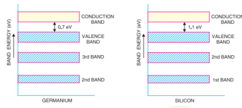
It may be seen that forbidden energy gap is very small; being 1.1 eV for silicon and 0.7 eV for germanium. Therefore, relatively small energy is needed by their valence electrons to cross over to the conduction band. Even at room temperature, some of the valence electrons may acquire sufficient energy to enter into the conduction band and thus become free electrons. However, at this temperature, the number of free electrons available is very small. Therefore, at room temperature, a piece of germanium or silicon is neither a good conductor nor an insulator. For this reason, such substances are called semiconductors. The energy band description is extremely helpful in understanding the current flow through a semiconductor.
Q4) Discuss the effect of temperature on semiconductors?
Answer:
The electrical conductivity of a semiconductor changes appreciably with temperature variations. This is a very important point to keep in mind.
(i) At absolute zero.
At absolute zero temperature, all the electrons are tightly held by the semiconductor atoms. The inner orbit electrons are bound whereas the valence electrons are engaged in co-valent bonding. At this temperature, the co-valent bonds are very strong and there are no free electrons. Therefore, the semiconductor crystal behaves as a perfect insulator .In terms of energy band description, the valence band is filled and there is a large energy gap between valence band and conduction band. Therefore, no valence electron can reach the conduction band to become free electron. It is due to the non-availability of free electrons that a semiconductor behaves as an insulator.
(ii) Above absolute zero.
When the temperature is raised, some of the covalent bonds in the semiconductor break due to the thermal energy supplied. The breaking of bonds sets those electrons free which are engaged in the formation of these bonds. The result is that a few free electrons exist in the semiconductor. These free electrons can constitute a tiny electric current if potential difference is
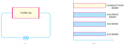
Applied across the semiconductor crystal. This shows that the resistance of a semiconductor decreases with the rise in temperature i.e. it has negative temperature coefficient of resistance. It may be added that at room temperature, current through a semiconductor is too small to be of any practical value.
Q.5 Define Fermi energy level. Explain Fermi Dirac distribution function ?
Answer:
When the material is at a temperature higher than OK, it receives thermal energy from surroundings i.e. electrons are thermally excited. As a result, they move into the higher energy levels which are unoccupied at OK. The occupation obeys a statistical distribution called Fermi – Dirac distribution law.
According to this distribution law, the probability F(E) that a given energy state E is occupied at a temperature T is given by

Here F(E) is called Fermi – Dirac probability function. It indicates that the fraction of all energy state (E) occupied under thermal equilibrium ‘K’ is Boltzmann constant.
Fermi Dirac distribution function:
Mathematically the probability of finding an electron in the energy state E at the temperature T is expressed as
Where, is the Boltzmann constant
T is the absolute temperature
Ef is the Fermi level or the Fermi energy
Now, let us try to understand the meaning of Fermi level. In order to accomplish this, put
in equation (1). By doing so, we get,
This means the Fermi level is the level at which one can expect the electron to be present exactly 50% of the time.
Q5) What do you understand by intrinsic and extrinsic semiconductors?
Answer:
Intrinsic semiconductor
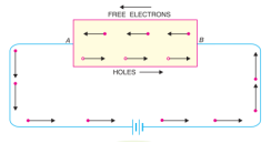
In an intrinsic semiconductor, even at room temperature, hole-electron pairs are created. When electric field is applied across an intrinsic semiconductor, the current conduction takes place by two processes, namely; by free electrons and holes. The free electrons are produced due to the breaking up of some covalent bonds by thermal energy. At the same time, holes are created in the covalent bonds. Under the influence of electric field, conduction through the semiconductor is by both free electrons and holes. Therefore, the total current inside the semiconductor is the sum of currents due to free electrons and holes.

Extrinsic semiconductor
The amount and type of such impurities have to be closely controlled during the preparation of extrinsic semiconductor.
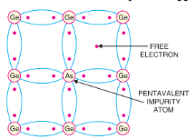
Generally, for 108 atoms of semiconductor, one impurity atom is added. The purpose of adding impurity is to increase either the number of free electrons or holes in the semiconductor crystal. As we shall see, if a pentavalent impurity (having 5 valence electrons) is added to the semiconductor, a large number of free electrons are produced in the semiconductor. On the other hand, addition of trivalent impurity (having 3 valence electrons) creates a large number of holes in the semiconductor crystal. Depending upon the type of impurity added,
Extrinsic semiconductors are classified into:
(i) n-type semiconductor
(ii) p-type semiconductor
Q6) What is a pn junction? Explain the formation of potential barrier in a pn junction.
Answer:
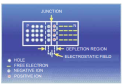
When a p-type semiconductor is suitably joined to n-type semiconductor, the contact surface is called pn junction.
Formation of pn junction. In actual practice, the characteristic properties of pn junction will not be apparent if a p-type block is just brought in contact with n-type block. In fact, pn junction is fabricated by special techniques. One common method of making pn junction is called alloying. In this method, a small block of indium (trivalent impurity) is placed on an n-type germanium slab
(i). The system is then heated to a temperature of about 500ºC. The indium and some of the germanium melt to form a small puddle of molten germanium-indium mixture
(ii). The temperature is then lowered and puddle begins to solidify. Under proper conditions, the atoms of indium impurity will be suitably adjusted in the germanium slab to form a single crystal. The addition of indium overcomes the excess of electrons in the n-type germanium to such an extent that it creates a p-type region.
Q. 8. Discuss the behavior of a pn junction under forward and reverse biasing.
Answer:
Forward biasing.
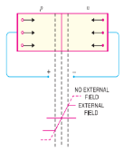
When external d.c. Voltage applied to the junction is in such a direction that it cancels the potential barrier, thus permitting current flow, it is called forward biasing. To apply forward bias, connect positive terminal of the battery to p-type and negative terminal to n-type. The applied forward potential establishes an electric field which acts against the field due to potential barrier. Therefore, the resultant field is weakened and the barrier height is reduced at the junction. As potential barrier voltage is very small (0.1 to 0.3 V), therefore, a small forward voltage is sufficient to completely eliminate the barrier. Once the potential barrier is eliminated by the forward voltage, junction resistance becomes almost zero and a low resistance path is established for the entire circuit. Therefore, current flows in the circuit. This is called forward current. With forward bias to pn junction, the following points are worth nothing:
(i) The potential barrier is reduced and at some forward voltage (0.1 to 0.3 V), it is eliminated altogether.
(ii) The junction offers low resistance (called forward resistance, Rf ) to current flow.
(iii) Current flows in the circuit due to the establishment of low resistance path. The magnitude of current depends upon the applied forward voltage.
Reverse biasing.

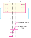
When the external d.c. Voltage applied to the junction is in such a direction that potential barrier is increased, it is called reverse biasing. To apply reverse bias, connect negative terminal of the battery to p-type and positive terminal to n-type as shown in Fig. 5.22. It is clear that applied reverse voltage establishes an electric field which acts in the same direction as the field due to potential barrier. Therefore, the resultant field at the junction is strengthened and the barrier height is increased. The increased potential barrier prevents the flow of charge carriers across the junction. Thus, a high resistance path is established for the entire circuit and hence the current does not flow. With reverse bias to pn junction, the following points are worth nothing:
(i) The potential barrier is increased.
(ii) The junction offers very high resistance (called reverse resistance, Rr ) to current flow.
(iii) No current flows in the circuit due to the establishment of high resistance path.
Q7) Draw and explain the V-I characteristics of a pn junction.
Answer:
Volt-ampere or V-I characteristic of a pn junction (also called a crystal or semiconductor diode) is the curve between voltage across the junction and the circuit current. Usually, voltage is taken along x axis and current along y-axis. Fig. 5.24 shows the *circuit arrangement for determining the V-I characteristics of a pn junction. The characteristics can be studied under three heads, namely; zero external voltage, forward bias and reverse bias.

(i) Zero external voltage. When the external voltage is zero, i.e. circuit is open at K, the potential barrier at the junction does not permit current flow. Therefore, the circuit current is zero as indicated by point O.

(ii) Forward bias- With forward bias to the pn junction i.e. p-type connected to positive terminal and n-type connected to negative terminal, the potential barrier is reduced. At some forward voltage (0.7 V for Si and 0.3 V for Ge), the potential barrier is altogether eliminated and current starts flowing in the circuit. From now onwards, the current increases with the increase in forward voltage. Thus, a rising curve OB is obtained with forward bias. From the forward characteristic, it is seen that at first (region OA),the current increases very slowly and the curve is non-linear. It is because the external applied voltage is used up in overcoming the potential barrier. However, once the external voltage exceeds the potential barrier voltage, the pn junction behaves like an ordinary conductor. Therefore, the current rises very sharply with increase in external voltage (region AB on the curve). The curve is almost linear.
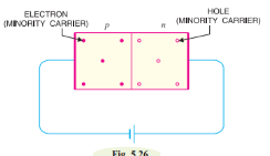
(iii) Reverse bias- With reverse bias to the pn junction i.e. p-type connected to negative terminal and n-type connected to positive terminal, potential barrier at the junction is increased. Therefore, the junction resistance becomes very high and practically no current flows through the circuit. However, in practice, a very small current (of the order of µA) flows in the circuit with reverse bias as shown in the reverse characteristic. This is called reverse *saturation current (Is ) and is due to the minority carriers. It may be recalled that there are a few free electrons in p-type material and a few holes in n-type material. These undesirable free electrons in p-type and holes in n-type are called minority carriers. These minority carriers, the applied reverse bias appears as forward bias.
If reverse voltage is increased continuously, the kinetic energy of electrons (minority carriers) may become high enough to knock out electrons from the semiconductor atoms. At this stage breakdown of the junction occurs, characterized by a sudden rise of reverse current and a sudden fall of the resistance of barrier region. This may destroy the junction permanently
.
Q .10. Explain Hall Effect in detail?
Answer:
When a material carrying current is subjected to a magnetic field in a direction perpendicular to direction of current, an electric field is developed across the material in a direction perpendicular to both the direction of magnetic field and current direction. This phenomenon is called “Hall-effect”.
Explanation:
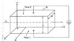
* Consider a semi-conductor, and current passes along the X-axis and a magnetic field Bz is applied along the Z-direction, a field Ey is called the Hall field which is developed in the Y-direction.
* In P- type semi-conductor, holes move with the velocity “V” in the “+”ve X-direction. As they move across the semiconductor the holes experience a transverse force ‘Bev’ due to the magnetic field.
* This force drives the holes down to the lower face. As a result, the lower face becomes +vely charged and –ve charge on the upper surface creating the hall field in the Y-direction. The Hall field exerts an upward force on holes equal to Ee.
* In the steady sate, two forces just balance and as a result, no further increase of + ve charge occurs on Face1.
* In N type semiconductor, the majority charge carriers are electrons experiences a force in the downward direction and lower face gets – vely charged. As a result, Hall field will be in the Y – direction.
Hall Coefficient:
Hall field𝐸𝐻, for a given material depends on the current density J and the applied magnetic field B.
i.e. 𝐸𝐻α JB
𝐸𝐻 = 𝑅𝐻 α JB
Since,

This is called hall coefficient.
UNIT 4
Question bank
Q1)What do you understand by a semi-conductor? Discuss some important properties of semiconductor
Answer:
A semiconductor is a substance which has resistivity (10−4 to 0.5 Ωm) in-between conductors and insulators e.g. Germanium, silicon, selenium, carbon etc.
Nichrome, which is one of the highest resistance materials, has resistivity much lower than germanium. This shows that electrically germanium cannot be regarded as a conductor or insulator or a resistance material. This gave such substances like germanium the name of semiconductors. It is interesting to note that it is not the resistivity alone that decides whether a substance is semiconductor or not. For example, it is just possible to prepare an alloy whose resistivity falls within the range of semiconductors but the alloy cannot be regarded as a semiconductor. In fact, semiconductors have a number of peculiar properties which distinguish them from conductors, insulators and resistance materials.
Properties of Semiconductors
(i) The resistivity of a semiconductor is less than an insulator but more than a conductor.
(ii) (ii) Semiconductors have negative temperature co-efficient of resistance i.e. the resistance of a semiconductor decreases with the increase in temperature and vice-versa. For example, germanium is actually an insulator at low temperatures but it becomes a good conductor at high temperatures.
(iii) (iii) When a suitable metallic impurity (e.g. Arsenic, gallium etc.) is added to a semiconductor, its current conducting properties change appreciably.
Q2)Which are the most commonly used semiconductors and why?
Answer:
The two most frequently used materials are germanium (Ge) and silicon (Si). It is because the energy required to break their co-valent bonds (i.e. energy required to release an electron from their valence bands) is very small; being about 0.7 eV for germanium and about 1.1 eV for silicon
Germanium. Germanium has become the model substance among the semiconductors; the main reason being that it can be purified relatively well and crystallised easily. Germanium is an earth element and was discovered in 1886. It is recovered from the ash of certain coals or from the flue dust of zinc smelters. Generally, recovered germanium is in the form of germanium dioxide powder which is then reduced to pure germanium.
The atomic number of germaniums is 32. Therefore, it has 32 protons and 32 electrons. Two electrons are in the first orbit, eight electrons in the second, eighteen electrons in the third and four electrons in the outer or valence orbit [See Fig. 5.2 (i)]. It is clear that germanium atom has four valence electrons i.e., it is a tetravalent element. Fig. 5.2 (ii) shows how the various germanium atoms are held through co-valent bonds. As the atoms are arranged in an orderly pattern, therefore, germanium has crystalline structure.
Silicon. Silicon is an element in most of the common rocks. Actually, sand is silicon dioxide. The silicon compounds are chemically reduced to silicon which is 100% pure for use as a semiconductor.
The atomic number of silicon is 14. Therefore, it has 14 protons and 14 electrons. Two electrons are in the first orbit, eight electrons in the second orbit and four electrons in the third orbit [See Fig. 5.3 (i)]. It is clear that silicon atom has four valence electrons i.e. it is a tetravalent element. Fig. 5.3 (ii) shows how various silicon atoms are held through co-valent bonds. Like germanium, silicon atoms are also arranged in an orderly manner. Therefore, silicon has crystalline structure.
Q3)Give the energy band description of semiconductors.
Answer:
In a semiconductor is a substance whose resistivity lies between conductors and insulators. The resistivity is of the order of 10−4 to 0.5-ohm meter. However, a semiconductor can be defined much more comprehensively on the basis of energy bands

It may be seen that forbidden energy gap is very small; being 1.1 eV for silicon and 0.7 eV for germanium. Therefore, relatively small energy is needed by their valence electrons to cross over to the conduction band. Even at room temperature, some of the valence electrons may acquire sufficient energy to enter into the conduction band and thus become free electrons. However, at this temperature, the number of free electrons available is very small. Therefore, at room temperature, a piece of germanium or silicon is neither a good conductor nor an insulator. For this reason, such substances are called semiconductors. The energy band description is extremely helpful in understanding the current flow through a semiconductor.
Q4) Discuss the effect of temperature on semiconductors?
Answer:
The electrical conductivity of a semiconductor changes appreciably with temperature variations. This is a very important point to keep in mind.
(i) At absolute zero.
At absolute zero temperature, all the electrons are tightly held by the semiconductor atoms. The inner orbit electrons are bound whereas the valence electrons are engaged in co-valent bonding. At this temperature, the co-valent bonds are very strong and there are no free electrons. Therefore, the semiconductor crystal behaves as a perfect insulator .In terms of energy band description, the valence band is filled and there is a large energy gap between valence band and conduction band. Therefore, no valence electron can reach the conduction band to become free electron. It is due to the non-availability of free electrons that a semiconductor behaves as an insulator.
(ii) Above absolute zero.
When the temperature is raised, some of the covalent bonds in the semiconductor break due to the thermal energy supplied. The breaking of bonds sets those electrons free which are engaged in the formation of these bonds. The result is that a few free electrons exist in the semiconductor. These free electrons can constitute a tiny electric current if potential difference is

Applied across the semiconductor crystal. This shows that the resistance of a semiconductor decreases with the rise in temperature i.e. it has negative temperature coefficient of resistance. It may be added that at room temperature, current through a semiconductor is too small to be of any practical value.
Q.5 Define Fermi energy level. Explain Fermi Dirac distribution function ?
Answer:
When the material is at a temperature higher than OK, it receives thermal energy from surroundings i.e. electrons are thermally excited. As a result, they move into the higher energy levels which are unoccupied at OK. The occupation obeys a statistical distribution called Fermi – Dirac distribution law.
According to this distribution law, the probability F(E) that a given energy state E is occupied at a temperature T is given by

Here F(E) is called Fermi – Dirac probability function. It indicates that the fraction of all energy state (E) occupied under thermal equilibrium ‘K’ is Boltzmann constant.
Fermi Dirac distribution function:
Mathematically the probability of finding an electron in the energy state E at the temperature T is expressed as
Where, is the Boltzmann constant
T is the absolute temperature
Ef is the Fermi level or the Fermi energy
Now, let us try to understand the meaning of Fermi level. In order to accomplish this, put
in equation (1). By doing so, we get,
This means the Fermi level is the level at which one can expect the electron to be present exactly 50% of the time.
Q5) What do you understand by intrinsic and extrinsic semiconductors?
Answer:
Intrinsic semiconductor
In an intrinsic semiconductor, even at room temperature, hole-electron pairs are created. When electric field is applied across an intrinsic semiconductor, the current conduction takes place by two processes, namely; by free electrons and holes. The free electrons are produced due to the breaking up of some covalent bonds by thermal energy. At the same time, holes are created in the covalent bonds. Under the influence of electric field, conduction through the semiconductor is by both free electrons and holes. Therefore, the total current inside the semiconductor is the sum of currents due to free electrons and holes.
Extrinsic semiconductor
The amount and type of such impurities have to be closely controlled during the preparation of extrinsic semiconductor.
Generally, for 108 atoms of semiconductor, one impurity atom is added. The purpose of adding impurity is to increase either the number of free electrons or holes in the semiconductor crystal. As we shall see, if a pentavalent impurity (having 5 valence electrons) is added to the semiconductor, a large number of free electrons are produced in the semiconductor. On the other hand, addition of trivalent impurity (having 3 valence electrons) creates a large number of holes in the semiconductor crystal. Depending upon the type of impurity added,
Extrinsic semiconductors are classified into:
(i) n-type semiconductor
(ii) p-type semiconductor

Q6) What is a pn junction? Explain the formation of potential barrier in a pn junction.
Answer:
When a p-type semiconductor is suitably joined to n-type semiconductor, the contact surface is called pn junction.
Formation of pn junction. In actual practice, the characteristic properties of pn junction will not be apparent if a p-type block is just brought in contact with n-type block. In fact, pn junction is fabricated by special techniques. One common method of making pn junction is called alloying. In this method, a small block of indium (trivalent impurity) is placed on an n-type germanium slab
(i). The system is then heated to a temperature of about 500ºC. The indium and some of the germanium melt to form a small puddle of molten germanium-indium mixture
(ii). The temperature is then lowered and puddle begins to solidify. Under proper conditions, the atoms of indium impurity will be suitably adjusted in the germanium slab to form a single crystal. The addition of indium overcomes the excess of electrons in the n-type germanium to such an extent that it creates a p-type region.

Q. 8. Discuss the behavior of a pn junction under forward and reverse biasing.
Answer:
Forward biasing.


When external d.c. Voltage applied to the junction is in such a direction that it cancels the potential barrier, thus permitting current flow, it is called forward biasing. To apply forward bias, connect positive terminal of the battery to p-type and negative terminal to n-type. The applied forward potential establishes an electric field which acts against the field due to potential barrier. Therefore, the resultant field is weakened and the barrier height is reduced at the junction. As potential barrier voltage is very small (0.1 to 0.3 V), therefore, a small forward voltage is sufficient to completely eliminate the barrier. Once the potential barrier is eliminated by the forward voltage, junction resistance becomes almost zero and a low resistance path is established for the entire circuit. Therefore, current flows in the circuit. This is called forward current. With forward bias to pn junction, the following points are worth nothing:
(i) The potential barrier is reduced and at some forward voltage (0.1 to 0.3 V), it is eliminated altogether.
(ii) The junction offers low resistance (called forward resistance, Rf ) to current flow.
(iii) Current flows in the circuit due to the establishment of low resistance path. The magnitude of current depends upon the applied forward voltage.
Reverse biasing.
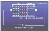
When the external d.c. Voltage applied to the junction is in such a direction that potential barrier is increased, it is called reverse biasing. To apply reverse bias, connect negative terminal of the battery to p-type and positive terminal to n-type as shown in Fig. 5.22. It is clear that applied reverse voltage establishes an electric field which acts in the same direction as the field due to potential barrier. Therefore, the resultant field at the junction is strengthened and the barrier height is increased. The increased potential barrier prevents the flow of charge carriers across the junction. Thus, a high resistance path is established for the entire circuit and hence the current does not flow. With reverse bias to pn junction, the following points are worth nothing:
(i) The potential barrier is increased.
(ii) The junction offers very high resistance (called reverse resistance, Rr ) to current flow.
(iii) No current flows in the circuit due to the establishment of high resistance path.
Q7) Draw and explain the V-I characteristics of a pn junction.
Answer:
Volt-ampere or V-I characteristic of a pn junction (also called a crystal or semiconductor diode) is the curve between voltage across the junction and the circuit current. Usually, voltage is taken along x axis and current along y-axis. Fig. 5.24 shows the *circuit arrangement for determining the V-I characteristics of a pn junction. The characteristics can be studied under three heads, namely; zero external voltage, forward bias and reverse bias.

(i) Zero external voltage. When the external voltage is zero, i.e. circuit is open at K, the potential barrier at the junction does not permit current flow. Therefore, the circuit current is zero as indicated by point O.
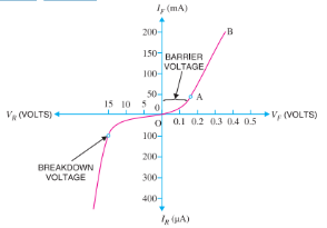
(ii) Forward bias- With forward bias to the pn junction i.e. p-type connected to positive terminal and n-type connected to negative terminal, the potential barrier is reduced. At some forward voltage (0.7 V for Si and 0.3 V for Ge), the potential barrier is altogether eliminated and current starts flowing in the circuit. From now onwards, the current increases with the increase in forward voltage. Thus, a rising curve OB is obtained with forward bias. From the forward characteristic, it is seen that at first (region OA),the current increases very slowly and the curve is non-linear. It is because the external applied voltage is used up in overcoming the potential barrier. However, once the external voltage exceeds the potential barrier voltage, the pn junction behaves like an ordinary conductor. Therefore, the current rises very sharply with increase in external voltage (region AB on the curve). The curve is almost linear.
(iii) Reverse bias- With reverse bias to the pn junction i.e. p-type connected to negative terminal and n-type connected to positive terminal, potential barrier at the junction is increased. Therefore, the junction resistance becomes very high and practically no current flows through the circuit. However, in practice, a very small current (of the order of µA) flows in the circuit with reverse bias as shown in the reverse characteristic. This is called reverse *saturation current (Is ) and is due to the minority carriers. It may be recalled that there are a few free electrons in p-type material and a few holes in n-type material. These undesirable free electrons in p-type and holes in n-type are called minority carriers. These minority carriers, the applied reverse bias appears as forward bias.
If reverse voltage is increased continuously, the kinetic energy of electrons (minority carriers) may become high enough to knock out electrons from the semiconductor atoms. At this stage breakdown of the junction occurs, characterized by a sudden rise of reverse current and a sudden fall of the resistance of barrier region. This may destroy the junction permanently
.
Q .10. Explain Hall Effect in detail?
Answer:
When a material carrying current is subjected to a magnetic field in a direction perpendicular to direction of current, an electric field is developed across the material in a direction perpendicular to both the direction of magnetic field and current direction. This phenomenon is called “Hall-effect”.
Explanation:
* Consider a semi-conductor, and current passes along the X-axis and a magnetic field Bz is applied along the Z-direction, a field Ey is called the Hall field which is developed in the Y-direction.
* In P- type semi-conductor, holes move with the velocity “V” in the “+”ve X-direction. As they move across the semiconductor the holes experience a transverse force ‘Bev’ due to the magnetic field.
* This force drives the holes down to the lower face. As a result, the lower face becomes +vely charged and –ve charge on the upper surface creating the hall field in the Y-direction. The Hall field exerts an upward force on holes equal to Ee.
* In the steady sate, two forces just balance and as a result, no further increase of + ve charge occurs on Face1.
* In N type semiconductor, the majority charge carriers are electrons experiences a force in the downward direction and lower face gets – vely charged. As a result, Hall field will be in the Y – direction.

Hall Coefficient:
Hall field𝐸𝐻, for a given material depends on the current density J and the applied magnetic field B.
i.e. 𝐸𝐻α JB
𝐸𝐻 = 𝑅𝐻 α JB
Since,
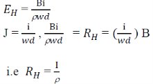
This is called hall coefficient.