Unit - 2
Combinational Circuit
Q1) Convert the Boolean function into Standard SoP form.
f = p’qr + pq’r + pqr’ + pqr
A1)
Step 1 – By using the Boolean postulate, x + x = x and also writing the last term pqr two more times we get
⇒ f = p’qr + pq’r + pqr’ + pqr + pqr + pqr
Step 2 – By Using Distributive law for 1st and 4th terms, 2nd and 5th terms, 3rdand 6th terms.
⇒ f = qr(p’ + p) + pr(q’ + q) + pq(r’ + r)
Step 3 – Then Using Boolean postulate, x + x’ = 1 we get
⇒ f = qr(1) + pr(1) + pq(1)
Step 4 – hence using Boolean postulate, x.1 = x we get
⇒ f = qr + pr + pq
⇒ f = pq + qr + pr
This is the required Boolean function.
Q2) Convert the Boolean function into Standard PoS form.
f = (p + q + r).(p + q + r’).(p + q’ + r).(p’ + q + r)
A2)
Step 1 – By using the Boolean postulate, x.x = x and writing the first term p+q+r two more times we get
⇒ f = (p + q + r).(p + q + r).(p + q + r).(p + q + r’).(p +q’ + r).(p’ + q + r)
Step 2 – Now by using Distributive law, x + (y.z) = (x + y).(x + z) for 1st and 4thparenthesis, 2nd and 5th parenthesis, 3rd and 6th parenthesis.
⇒ f = (p + q + rr’).(p + r + qq’).(q + r + pp’)
Step 3 − Applying Boolean postulate, x.x’=0 for simplifying of the terms present in each parenthesis.
⇒ f = (p + q + 0).(p + r + 0).(q + r + 0)
Step 4 − Using Boolean postulate, x + 0 = x we get
⇒ f = (p + q).(p + r).(q + r)
⇒ f = (p + q).(q + r).(p + r)
This is the simplified Boolean function.
Hence, both Standard SoP and Standard PoS forms are Dual to one another.
Q3) What is a combinational circuit?
A3) A Combinational circuit is a circuit in which we combine the different gates. For example encoder, decoder, multiplexer, demultiplexer etc. Some of the characteristics are as follows −
- The output of combinational circuit depends only on the levels present at input terminals at any instant of time.
- It does not use any memory element. Therefore, the previous state of input does not have any effect on the present state of the circuit.
- It can have n number of inputs and m number of outputs.
Block diagram
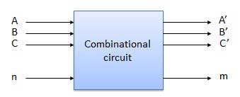
Fig. 1: Combinational circuit (ref.2)
Q4) Simplify f(X,Y,Z)=∏M(0,1,2,4)f(X,Y,Z)=∏M(0,1,2,4)using K-map.

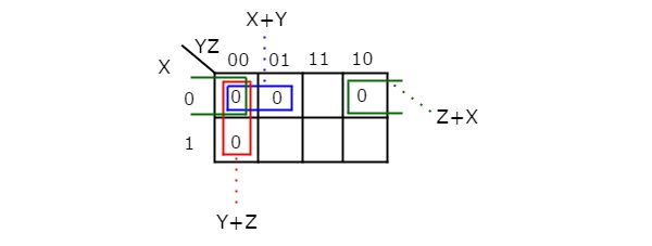
Therefore, the simplified Boolean function is
f = (X + Y).(Y + Z).(Z + X)
Q5) Simplify: F(P,Q,R,S)=∑(0,2,5,7,8,10,13,15)
A5)
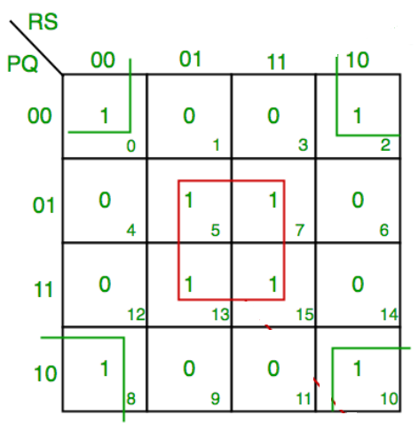
F = P’Q’R’S’ + PQ’R’S’ + P’Q’RS’ +PQ’RS’ + QS
F = P’Q’S’ + PQ’S’ + QS
F = Q’S’ +QS
Q6) Simplify: F(A,B,C)=π(0,3,6,7)
A6)
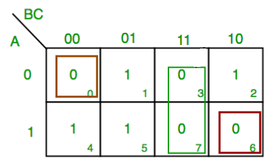
F = A’BC +ABC +A’B’C’ +ABC’
F = BC + C’ (A’B’ + AB)
Q7) Explain half adder with truth table and logic diagram?
A7)
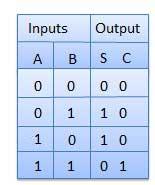
It is a combinational circuit which has two inputs and two outputs.
It is designed to add two single bit binary number A and B.
It has two outputs carry and sum.
Block diagram
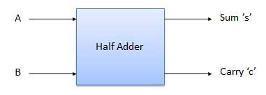
Fig.2: Half adder (ref. 2)
Truth Table
Circuit Diagram
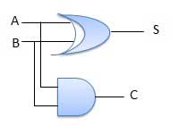
Fig.3: Half adder
Q8) Explain 4-bit parallel adder?
A8)
Here, A0 and B0 represent the LSB of the four bit words A and B.
Hence Adder-0 is the lowest stage.
Cin is considered 0.
The rest of the connections are same as that of n-bit parallel adder.
It is a very common logic circuit.
Block diagram
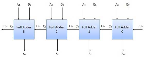
Fig.4: 4 bit parallel adder
Q9) Explain the internal diagram of look ahead carry adder?
A9)
- In this, for each adder block, the two bits that are to be added are available instantly.
- However, each of them waits for the carry to arrive from the previous one.
- So, it is impossible to generate the sum and carry of any block until the input carry is known.
- The block waits for the previous block to produce its carry. So there will be a considerable time delay which is known as carry propagation delay.

Fig 5: Look ahead Carry adder (ref. 2)
- Here, the sum is produced by the corresponding full adder as soon as the input signals are applied to it. The carry must propagate to all the stages so that output and carry settle their final steady-state value.
- The propagation time is equal to the propagation delay of each adder block, multiplied by the number of adder blocks in the circuit.
- It reduces the propagation delay by introducing more complex hardware.
- The ripple carry design is suitably transformed in such a way that the carry logic over fixed groups of bits is reduced to two-level logic.
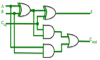
Fig.6: Look ahead Carry adder (ref. 2)

Q10) What are line decoders explain?
A10)
- It works as an inverse of an encoder.
- It is a combinational circuit which converts n input lines into 2n output lines.
- Taking an example of 3-to-8 line decoder.
Truth Table –
X | Y | Z | D0 | D1 | D2 | D3 | D4 | D5 | D6 | D7 |
0 | 0 | 0 | 1 | 0 | 0 | 0 | 0 | 0 | 0 | 0 |
0 | 0 | 1 | 0 | 1 | 0 | 0 | 0 | 0 | 0 | 0 |
0 | 1 | 0 | 0 | 0 | 1 | 0 | 0 | 0 | 0 | 0 |
0 | 1 | 1 | 0 | 0 | 0 | 1 | 0 | 0 | 0 | 0 |
1 | 0 | 0 | 0 | 0 | 0 | 0 | 1 | 0 | 0 | 0 |
1 | 0 | 1 | 0 | 0 | 0 | 0 | 0 | 1 | 0 | 0 |
1 | 1 | 0 | 0 | 0 | 0 | 0 | 0 | 0 | 1 | 0 |
1 | 1 | 1 | 0 | 0 | 0 | 0 | 0 | 0 | 0 | 1 |
Implementation
D0 is high when X = 0, Y = 0 and Z = 0. Hence,
D0 = X’ Y’ Z’
Similarly,
D1 = X’ Y’ Z
D2 = X’ Y Z’
D3 = X’ Y Z
D4 = X Y’ Z’
D5 = X Y’ Z
D6 = X Y Z’
D7 = X Y Z
Hence,
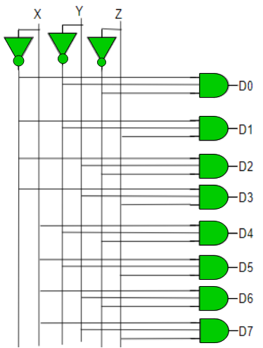
Fig 7. Decoder
Q11) Explain the implementation of encoder?
A11)
- It is a combinational circuit that converts binary information in the form of a 2N input lines into N output lines, which represent N bit code for the input.
- For simple encoders, only one input line is active at a time.
- For example: Octal to Binary encoder takes 8 input lines and generates 3 output lines.
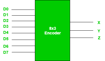
Fig.8: 8X3 Encoder (ref. 2)
Truth Table –
D7 | D6 | D5 | D4 | D3 | D2 | D1 | D0 | X | Y | Z |
0 | 0 | 0 | 0 | 0 | 0 | 0 | 1 | 0 | 0 | 0 |
0 | 0 | 0 | 0 | 0 | 0 | 1 | 0 | 0 | 0 | 1 |
0 | 0 | 0 | 0 | 0 | 1 | 0 | 0 | 0 | 1 | 0 |
0 | 0 | 0 | 0 | 1 | 0 | 0 | 0 | 0 | 1 | 1 |
0 | 0 | 0 | 1 | 0 | 0 | 0 | 0 | 1 | 0 | 0 |
0 | 0 | 1 | 0 | 0 | 0 | 0 | 0 | 1 | 0 | 1 |
0 | 1 | 0 | 0 | 0 | 0 | 0 | 0 | 1 | 1 | 0 |
1 | 0 | 0 | 0 | 0 | 0 | 0 | 0 | 1 | 1 | 1 |
- From the above truth table it is seen that the output is 000 when D0 is active; 001 when D1 is active; 010 when D2 is active and so on.
Implementation –
- From the above truth table, the output Z is active when the input octal digit is 1, 3, 5 or 7.
- Y is active when input octal digit is 2, 3, 6 or 7 and X is active when input octal digits 4, 5, 6 or 7.
- Hence, the Boolean functions would be:
X = D4 + D5 + D6 + D7
Y = D2 +D3 + D6 + D7
Z = D1 + D3 + D5 + D7
- Hence, the encoder is realised with OR gates as follows:
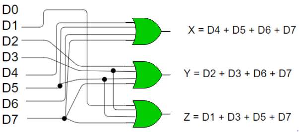
Fig 9: 8:3 encoder
Limitation of the encoder is that only one input is active at a time.
- If more than one input are active, then the output of encoder is undefined.
- For example, if D6 and D3 are both active, then, our output would be 111 which is the output for D7.
- Problem arises when all inputs are 0.
- The encoder gives output 000 which actually is the output for D0. To avoid this, an extra bit is added to the output which is called the valid bit whose value is 0 when all inputs are 0 or 1.
Q12) Explain the logic diagram of multiplexer?
A12)
- It is a special type of combinational circuit.
- It has n-data inputs, one output and m inputs select lines with 2m = n.
- It selects one of the n data inputs and routes it to the output.
- The selection of one of the inputs is done by the select lines.
- Depending on the code applied at the inputs, one of the n data sources is selected and transmitted to the single output Y.
- E is the enable input which is useful for cascading purpose.
- It is an active low terminal hence performs the required operation when it is low.

Fig 10: Block diagram of multiplexer (ref. 2)
Multiplexers come in multiple variations
- 2 : 1 multiplexer
- 4 : 1 multiplexer
- 16 : 1 multiplexer
- 32 : 1 multiplexer
Block Diagram of 2:1 MUX
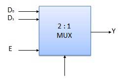
Truth Table of 2:1 MUX
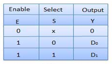
Where x is don’t care.
Q13) What are demultiplexers?
A13)
- It performs the inverse operation of a multiplexer as it receives one input and distributes it across its outputs.
- It has only one input and n outputs with m select input.
- At a time only one output line is selected by the select lines and that input is transmitted through the output line.
- It is equivalent to a single pole multiple way switch.
Various Demultiplexers are used as:
- 1: 2 demultiplexer
- 1: 4 demultiplexer
- 1: 16 demultiplexer
- 1: 32 demultiplexer
Block diagram
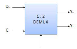
Truth Table
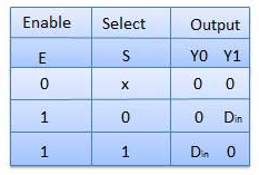
Where x is don’t care.
Q14) Realize all the logic gates using NAND gate?
A14)
Implementing an inverter using NAND gate
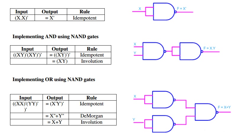

Fig 11: Implementation of basic gates using NAND gate
Q15) Realize logic gates using NOR gate?
A15)
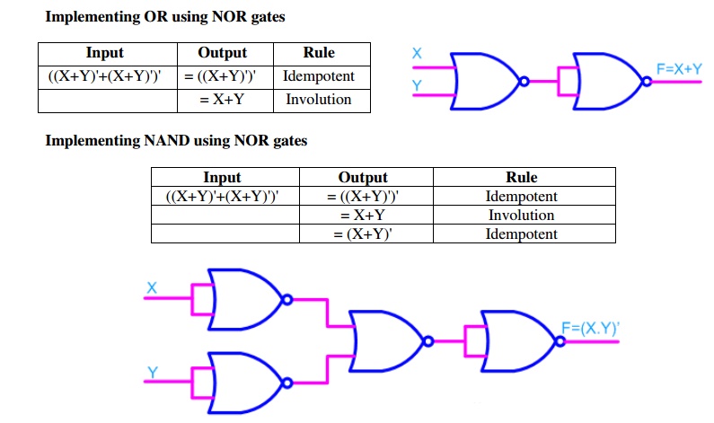
Fig 12: Implementation of Or and NAND gate using NOR gate
Q16) Explain Parity checker with truth table and logic diagram?
Parity Checker
- They are of two types:
- Even parity checker: It checks error in the transmitted data, which contains message bits along with even parity.
- Odd parity checker: It checks error in the transmitted data, which contains message bits along with odd parity.
Even parity checker
Assume a 3-bit binary input, W, X and Y is transmitted along with an even parity bit, P. So, the resultant data contains 4 bits, that is received as the input of even parity checker.
It generates an even parity bit, E. This bit is zero, if the received data contains an even number of ones, which indicates that there is no error in the received data and vice versa.
The Truth table of an even parity checker is:
4-bit Received Data WXYP | Even Parity Check bit E |
0000 | 0 |
0001 | 1 |
0010 | 1 |
0011 | 0 |
0100 | 1 |
0101 | 0 |
0110 | 0 |
0111 | 1 |
1000 | 1 |
1001 | 0 |
1010 | 0 |
1011 | 1 |
1100 | 0 |
1101 | 1 |
1110 | 1 |
1111 | 0 |
The Boolean function of even parity check bit as
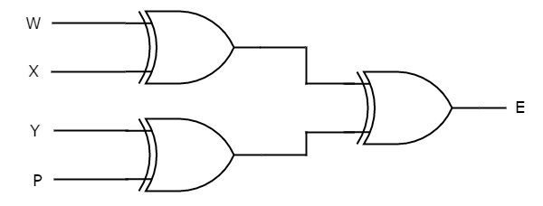
E = W xor X xor Y xor P
The following figure shows the circuit diagram of even parity checker.
Odd Parity Checker
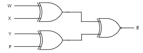
Assume a 3-bit binary input, W, X and Y is transmitted along with an odd parity bit, P. So, the resultant data contains 4 bits, that is received as the input of odd parity checker.
It generates an odd parity bit, E. This bit is zero, if the received data contains an odd number of ones, which indicates there is no error in the received data.
Q17) What are Tree Mux. Explain with logic diagrams?
A Tree MUX connects a common to a set of output (or input) connections using SPDT relays. The signal is switched using a tree structure to expand the number of output connections supported. Since the relay is used to select which of two paths is closed the MUX only permits one overall path to be selected, and there is no possibility of unintentionally connecting output connections together.
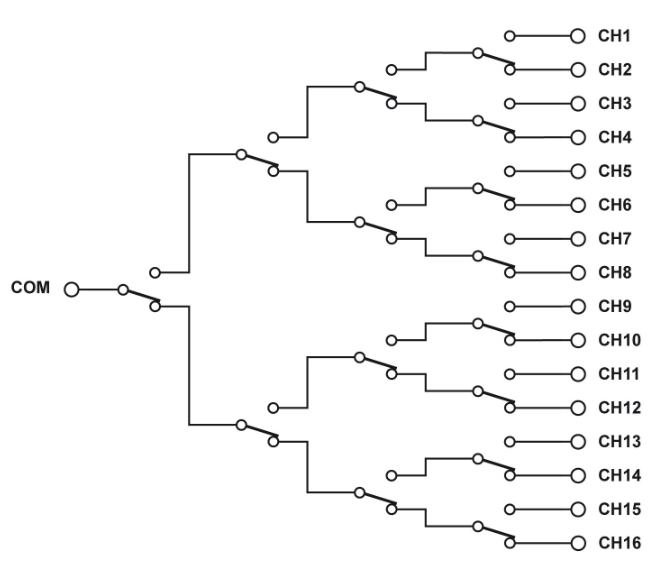
The path uses a number of relays in series so DC resistance of the thru path is higher than in a conventional MUX.
The number of relays required in the MUX is higher than a conventional MUX. Unless additional relays are added Tree MUX's always have a default path between the common and one output.
However, the MUX BW is considerably higher since the paths do not have open circuit traces or other relays connected to them that create transmission line stubs, so they have the best possible BW that the relays can provide.
Tree MUX's are often used as part of RF matrices in order to provide wide RF BW Tree and Crosspoint Matrices, at no point are there excess tracks connected to the RF path which minimises excess capacitive. A second use is in power systems where the input is to only be connected to one output, even in the event of a relay weld. As the MUX is created from changeover switches a welded relay inherently prevents an additional path from being connected.
Q18) Explain BCD to 7 segment decoders?
A18)
In most practical applications, seven segment displays are used to give a visual indication of the output states of digital IC’s such a decade counters, latches etc. For using this display device, the data has to be converted from some binary code to the code required for the display. Usually, the binary code used is natural BCD.
The following figure shows the display device and the segments which must be illuminated for each of the numerals.

The display system can be connected as follows:
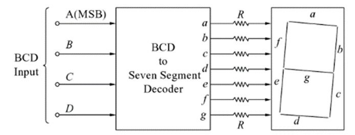
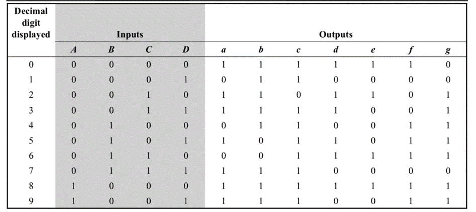
Here, ABCD is the natural BCD code for numerals 0 through 9. Following is the truth table of BCD to 7-segment decoder
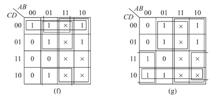
The K-Maps for each of the outputs A through G are given below:
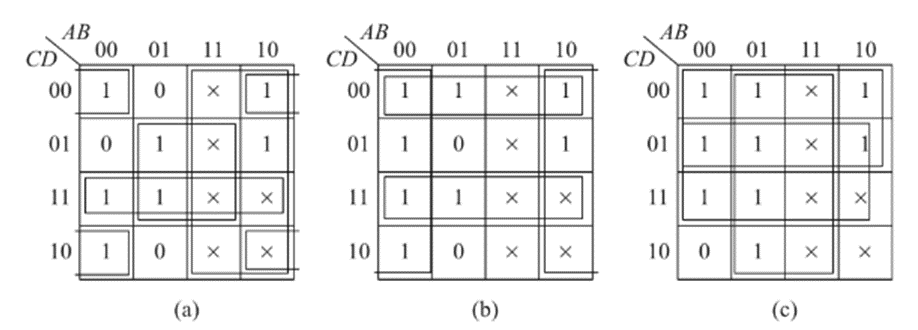

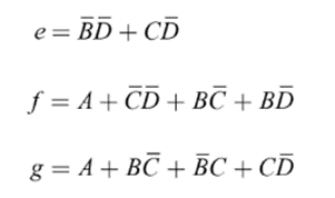
The simplified expressions obtained from the k-maps are:

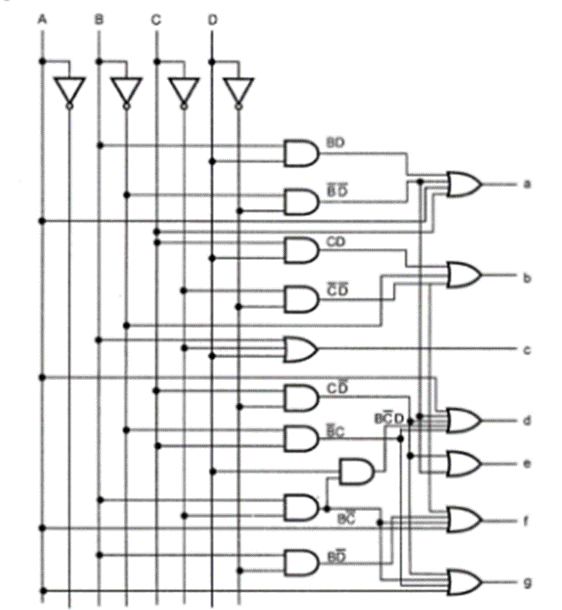
Logic diagram:
Q19) What are digital comparators?
A19)
- It performs comparison operation with more than four bits by cascading two or more 4-bit comparators.
- When two comparators are to be cascaded, the outputs of the lower-order comparator is connected to corresponding input of the higher-order comparator.
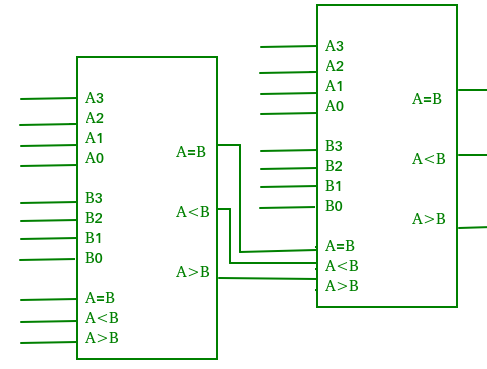
Fig 13. Digital comparator
Applications of Comparators –
- They are used in central processing units (CPUs) and microcontrollers (MCUs).
- They are used in control applications where the binary numbers represent physical variables such as temperature, position, etc. and are compared with a reference value.
- They are also used as process controllers and Servo motor controllers.
- They are used in password verification and biometric applications too.