Unit - 3
Sequential Logic Design
Q1) What are sequential circuits?
A1)
- A Sequential circuit consists of inputs variable (X), logic gates and output variable (Z).
- Combinational circuit generates an output on the basis of input variable only but Sequential circuit produces an output based on current input and previous output variables.
- This means that it includes memory elements which are capable of storing binary information.
- This binary information is nothing but the state of the sequential circuit at any given time. A latch capable of storing one bit information.

Fig. Combinational circuit
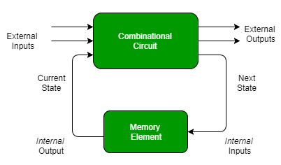
Fig. Sequential circuit
There are two types of input to the combinational logic in fig 2:
- External inputs which are not controlled by the circuit.
- Internal inputs which are function of previous output states.
Secondary inputs are state variables that are produced by the storage elements whereas secondary outputs are excitations for those storage elements.
Q2) What are the types of sequential circuits?
A2) There are two types of sequential circuit:
Asynchronous sequential circuit –
- They do not use a clock signal but instead uses the pulses as inputs.
- These circuits are faster because there is clock pulse and can change their state immediately when there is a change in the input signal.
- It is used when speed of operation is important and is independent of internal clock pulse.

Fig. Asynchronous Sequential circuit
But they are more difficult to design and their output is also uncertain.
Synchronous sequential circuit –
- These circuit uses clock signal and level inputs.
- The output pulse is received in the same duration as the clock pulse for the clocked sequential circuits.
- They wait for the next clock pulse to arrive to perform the next operation, these circuits are bit slower as compared to asynchronous circuits.
- Level output changes state at the start of an input pulse and remains in that state until the next input or clock pulse arrives.
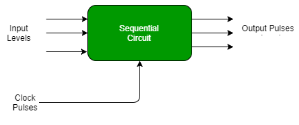
Fig. Synchronous Sequential circuit
- It is used in synchronous counters, flip flops, and in MOORE-MEALY machines.
- It is also used to design Counters, Registers, RAM, etc
Q3) Write truth table for SR latch?
A3) SR Latch is a circuit which has:
(i) 2 cross-coupled NOR gate or NAND gate.
(ii) 2 input S for SET and R for RESET.
(iii) 2 output Q and Q’.
Q | Q’ | STATE |
1 | 0 | Set |
0 | 1 | Reset |
Under normal conditions, both the input remains 0.
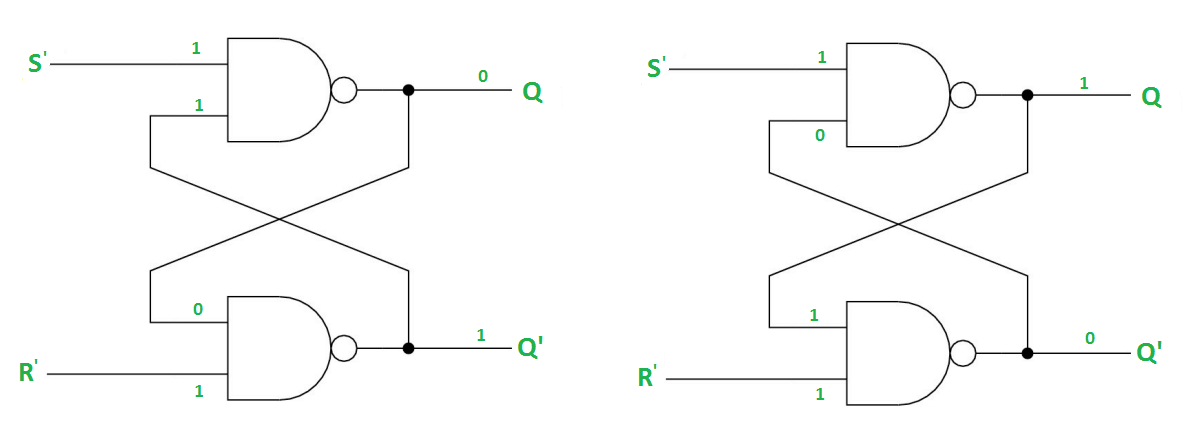
RS Latch with NAND gates:
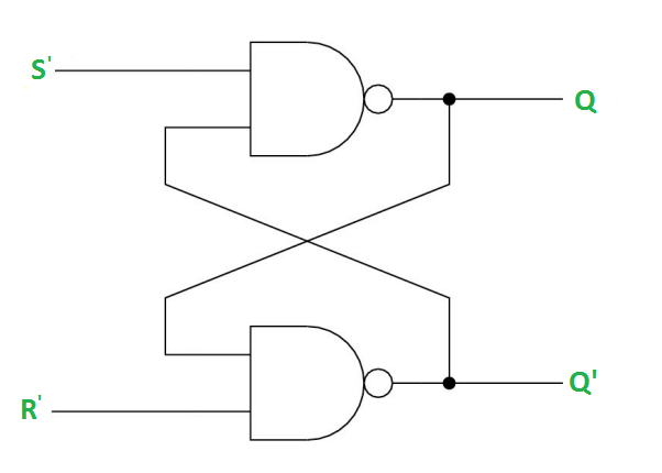
Case-1: When S’=R’=1 or S=R=0 then
If Q = 1, Q = R’ = 1.
If Q = 0, Q = 0 and R’ = 1 respectively.
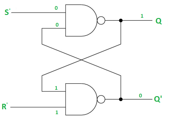
Case-2: S’=0, R’=1 (S=1, R=0)
As S’=0, Q = 1(SET state).
In 2nd NAND gate, as Q = R’ = 1, Q’=0.
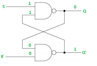
Case-3: S’= 1, R’= 0 (S=0, R=1)
As R’=0, Q’ = 1.
In 1st NAND gate, as Q =S’ = 1, Q=0 (RESET state).
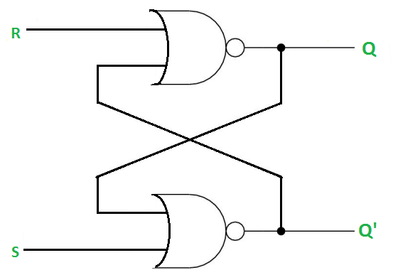
Case-4: S’= R’= 0 (S=R=1)
When S=R=1, both Q = Q’ = 1 which is not allowed.
So, this input condition is prohibited.
The SR Latch using NOR gate is:
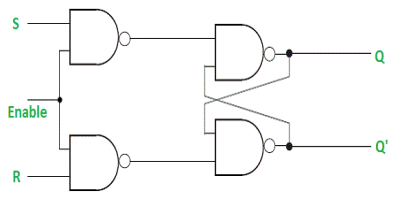
Q4) Explain the gated SR latch with circuit diagram?
A4) It is a latch which enable input that works when enable = 1 and retain the previous state when enable = 0.
Q5) Using NAND gates explain the gated D latch?
A5) It is similar to SR latch with little modifications. Here, the inputs are complements of one another. The design of D latch with Enable signal is given below:

The truth table is shown below:
ENABLE | D | Q(N) | Q(N+1) | STATE |
1 | 0 | x | 0 | RESET |
1 | 1 | x | 1 | SET |
0 | x | x | Q(n) | No Change |
As the output is same as input, it is also known as Transparent Latch.
The characteristic equation for D latch with enables input is given as:
Q(n+1) = EN.D + EN'.Q(n)
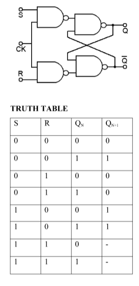
Q6) Explain SR flip flop with logic diagram and truth table?
A6) S-R Flip Flop:
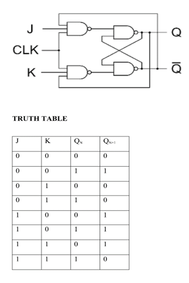
Q7) Explain the truth table and logic diagram of JK flip flop?
A7) J-K Flip Flop:
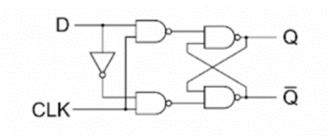
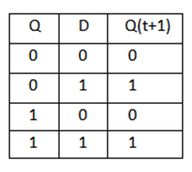
Q8) Explain the truth table and logic diagram of D flip flop?
A8) D Flip Flop:
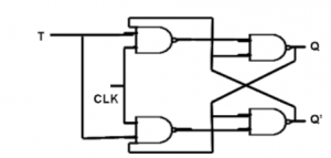
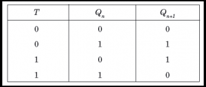
Q9) Explain the truth table and logic diagram of T flip flop?
A9)
Q10) What is race around condition?
A10) Race Around Condition in JK Flip-flop –
- For J-K flip-flop, if J=K=1, and if clk=1 for a long period of time, then output Q will toggle as long as CLK remains high which makes the output unstable or uncertain.
- This problem is known as race around condition in J-K flip-flop.
- This problem can be avoided by ensuring that the clock input is at logic “1” only for a very short time.
- Hence the concept of Master Slave JK flip flop was introduced.
Q11) How can we overcome the race around condition in JK flip flop?
A11) Master Slave JK flip flop –
It is basically a combination of two JK flip-flops connected together in series.
The first is the “master” and the other is a “slave”.
The output from the master is connected to the two inputs of the slave whose output is fed back to inputs of the master.
In addition to these two flip-flops, the circuit comprises of an inverter.
The inverter is connected to clock pulse in such a way that an inverted clock pulse is given to the slave flip-flop.
In other words, if CP=0 for a master flip-flop, then CP=1 for a slave flip-flop and vice versa.

Fig. Master Slave Flip flop
Working of a master slave flip flop –
- When the clock pulse goes high, the slave is isolated; J and K inputs can affect the state of the system. The slave flip-flop is isolated when the CP goes low. When the CP goes back to 0, information is transmitted from the master flip-flop to the slave flip-flop and output is obtained.
- The master flip flop is positive level triggered and the slave flip flop is negative level triggered, hence the master responds prior to the slave.
- If J=0 and K=1, Q’ = 1 then the master goes to the K input of the slave and the clock forces the slave to reset therefore the slave copies the master.
- If J=1 and K=0, Q = 1 then the master goes to the J input of the slave and the Negative transition of the clock sets the slave and thus copy the master.
- If J=1 and K=1, the master toggles on the positive transition and the slave toggles on the negative transition of the clock.
- If J=0 and K=0, the flip flop becomes disabled and Q remains unchanged.
Q12) Explain the timing diagram of Master Slave JK flip flop?
A12) Timing Diagram of a Master flip flop –
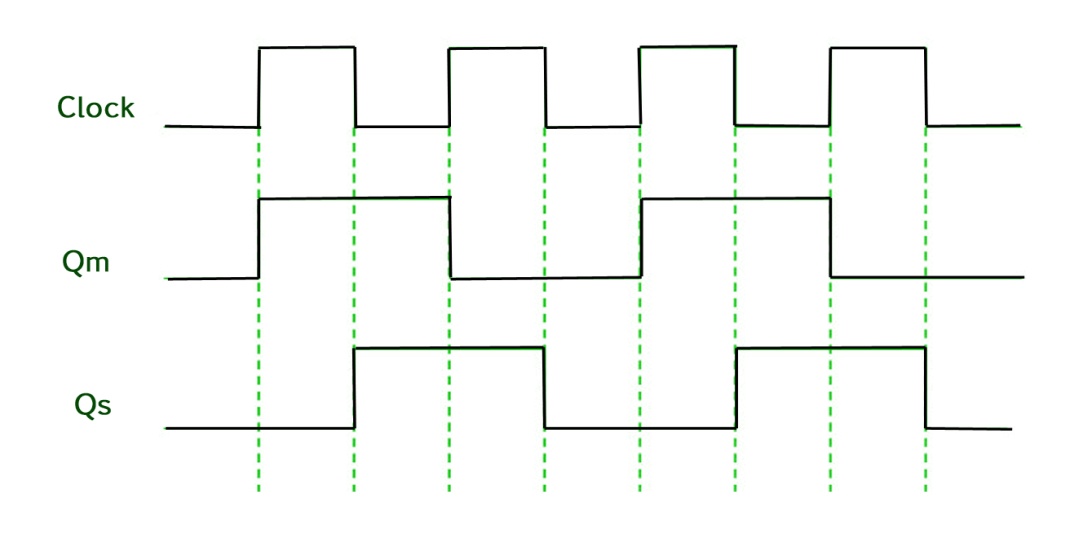
- When the CP = 1 then the output of master is high and remains high till CP = 0 because the state is stored.
- Now the output of master becomes low when the clock CP = 1 and remains low until the clock becomes high again.
- Thus, toggling takes place for a clock cycle.
- When the CP = 1 then the master is operational but not the slave.
- When the clock is low, the slave becomes operational and remains high until the clock again becomes low.
- Toggling takes place during the whole process since the output changes once in a cycle.
- This makes the Master-Slave J-K flip flop a Synchronous device which passes data with the clock signal.
Q13) What are state table and state diagrams in flip flops?
A13) State Table
The state table representation of a sequential circuit consists of three sections labeled present state, next state and output. The present state designates the state of flip-flops before the occurrence of a clock pulse. The next state shows the states of flip-flops after the clock pulse, and the output section lists the value of the output variables during the present state.
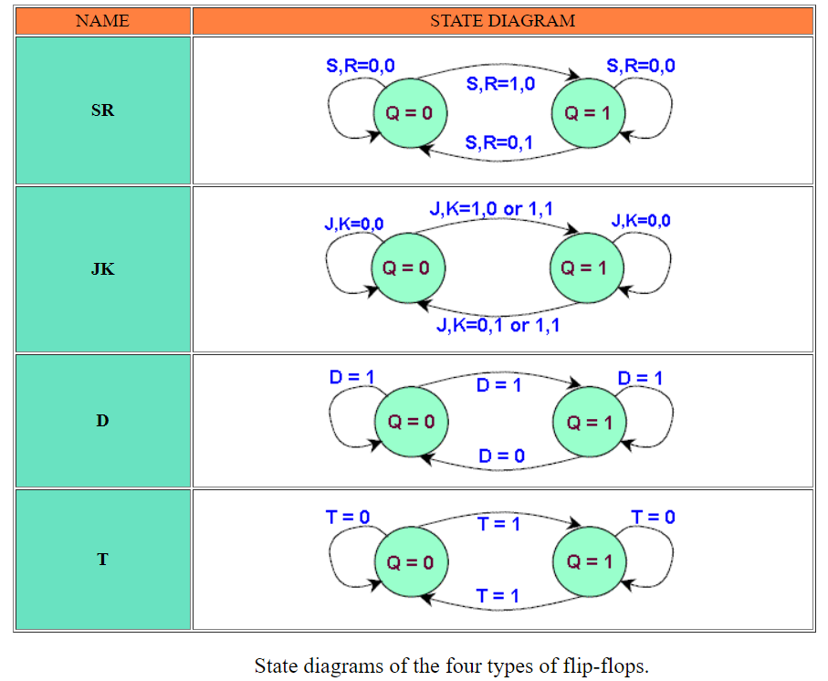
State Diagram
In addition to graphical symbols, tables or equations, flip-flops can also be represented graphically by a state diagram. In this diagram, a state is represented by a circle, and the transition between states is indicated by directed lines (or arcs) connecting the circles.
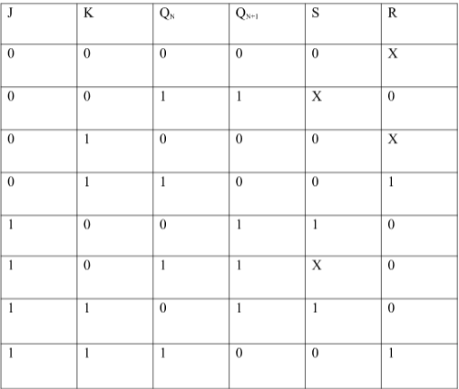
Q14) Convert SR to JK flip flop write the conversion table?
A14) SR To JK FlipFlop
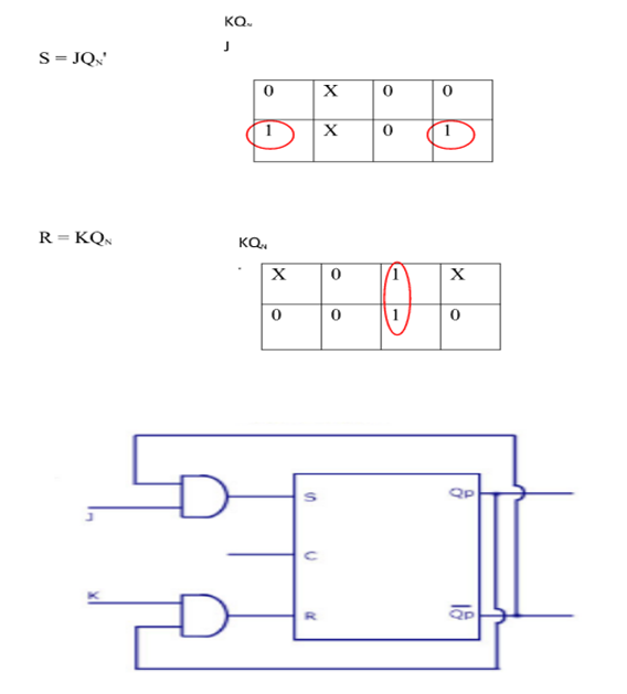
Excitation Functions:
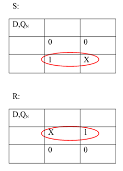
Q15) Write the excitation table for conversion of SR to D flip flop?
A15) Convert SR To D Flip-Flop:
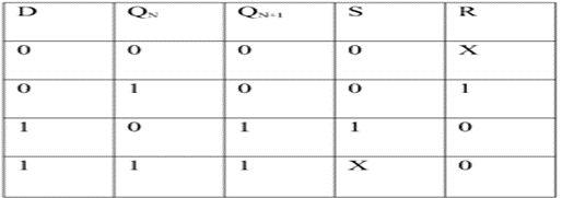
Excitation Functions:
S = D
R = D‘

Q16) Explain SISO and SIPO shift registers?
A16)
Serial-In Serial-Out Shift Register (SISO) –
- It allows serial input i.e. one bit after another and produces a serial output is known as Serial-In Serial-Out shift register.
- Since it has one output, the data leaves the register one bit at a time in a serial pattern, hence known as Serial-In Serial-Out Shift Register.
- The logic circuit is given underneath.
- The circuit comprises four D flip-flops which are connected serially.
- All these flip-flops are synchronous.

Fig. SISO
Serial-In Parallel-Out shift Register (SIPO) –
- It allows serial input through a single data line and produces a parallel output.
- The logic circuit is given underneath.
- The circuit consists of four D flip-flops which are connected synchronously.
- The clear (CLR) signal is also connected to all the 4 flip flops to RESET them.
- The output of the first flip flop is sent to the input of the next and so on.
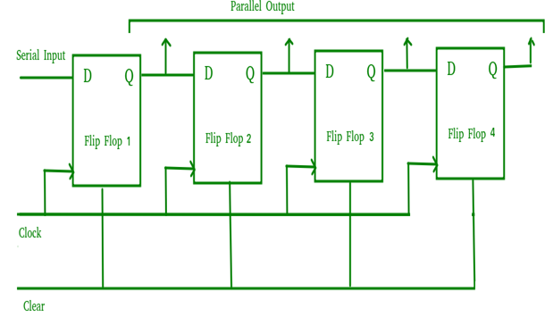
Fig. SIPO
- They are used in communication lines because the main use of the SIPO register is to convert serial data into parallel data.
Q17) Explain PIPO and PISO shift registers?
A17)
Parallel-In Serial-Out Shift Register (PISO) –
- It allows parallel input data and produces a serial output.
- The logic circuit is given underneath.
- The circuit comprises four D flip-flops which are connected synchronously.
- The clock is connected to all the flip flops but the input data is connected to each flip flop individually through a multiplexer.
- The output of the previous flip flop and parallel data input are connected to the input of the MUX and the output of MUX is connected to the next flip flop.
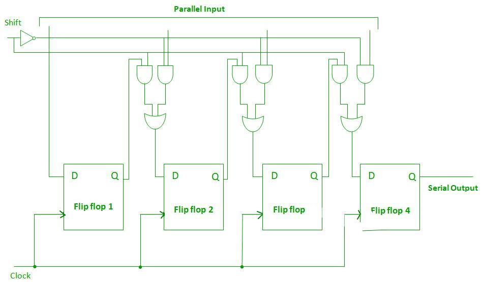
Fig. PISO
- It used to convert parallel data to serial data.
Parallel-In Parallel-Out Shift Register (PIPO) –
- It allows parallel input data and produces a parallel output.
- The logic circuit is given underneath.
- The circuit comprises four D flip-flops which are connected synchronously.
- The clear (CLR) and clock signals are connected to all flip flops.
- In this, there are no interconnections between flip-flops as no serial shifting of the data is required.
- Data is provided separately as input for each flip flop and the output is also collected individually from each flip flop.
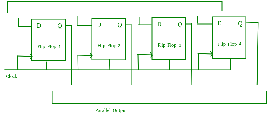
Fig. PIPO
- It is used as a temporary storage device and it acts as a delay element too.
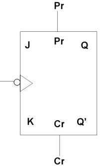
Q18) Explain the use of pre-set and clear terminals of flip flops?
A18)
As flip flop may come up in random states when power is switched on, it is necessary to use some method where all the flip flops can be set or reset at the same time by a single switch – it is inconvenient to set or reset each flip flop individually. This is achieved by incorporating PRESET and CLEAR inputs in flip flops which can over-write all other inputs. These I/Ps are asynchronous and independent of the clock. While they are present, all other operations are inhibited. They force the output to a certain state irrespective of the I/Ps and clock.
Active High
Active High means that Preset and Clear I/Ps are inactive when low.
Pr = 1, Q = 1, Q’ = 0
i.e. if the Preset I/P is 1, the output will be forced to SET state irrespective of other I/Ps.
Cr = 1, Q = 0, Q’ = 1
i.e. if the Clear I/P is 1, the output will be forced to RESET state irrespective of other I/Ps.
It is not possible to Preset and Clear a flip flop at the same instant of time as Q can’t be 0 and 1 at the same time.
i.e. Pr = Cr ≠ 1 at any instant.
