Unit - 1
Introduction to Operational Amplifier
Q1) Estimate dc emitter current in each transistor of differential amplifier shown in fig. How much is dc voltage from each collector to ground? How much is Vout?

A1)
The tail current through 24k resistor is,


The emitter current, IE, in each transistor is


Since IC = IE, voltage summation in the output circuit gives,


Then

Q2) Design an inverter amplifier with gain of 120 and input impedance of 5kΩ. Give the circuit.
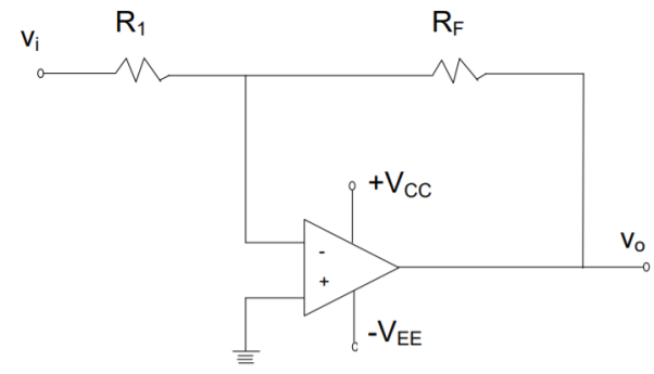
A2)
Figure shows the circuit for an inverting amplifier.
Since for an inverting amplifier, the input impedance Zi is,
Zi = R1 = 5kΩ (desired)
Therefore, R1 = 5kΩ Further, the gain AV of inverting amplifier is,
Av =RF/Ri
And, AV desired is 120, R1 = 5kΩ
Therefore, RF = AV x R1 = 120 X 5k= 600 kΩ
Q3) Find out the voltage gain of the non-inverting amplifier shown in fig.
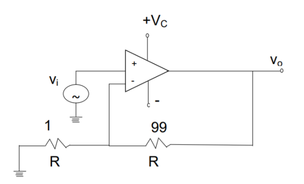
A3)
The voltage gain of a non-inverting amplifier is,


Q4) In the amplifier circuit shown in fig., if open loop gain and open loop band width of the op amp respectively are 105 and 10 HZ, Calculate the bandwidth of feedback amplifier
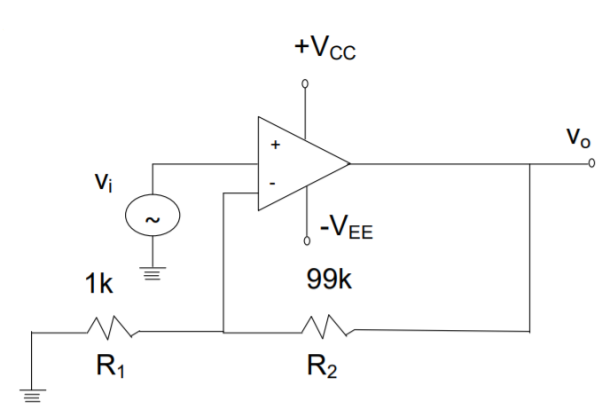
A4)
If open loop band width is f2, the band width with feedback, f2(FB) is given by f2(FB) = f2(1 + AB) ≈ f2. AB because AB>>1 Now, A = 105 (given) And the gain of feedback network, B in the circuit shown in fig. Is
And the gain of feedback network, B in the circuit shown in fig. Is

Then,


Q5) For the summing amplifier shown in fig., estimate the values of resistors R1, R2 and R3 so that the output V0 is, V0 = - (3V1 + V2 + 0.2V3). What is the approximate value of the compensating resistor R?

A5)
The output voltage,  for the summing amplifier is,

Thus for the desired output,

Similarly,


And 


And


Q6) Determine the output voltage in the circuit shown in fig. If Va= 5V, Vb= -2V and Vc = 3b
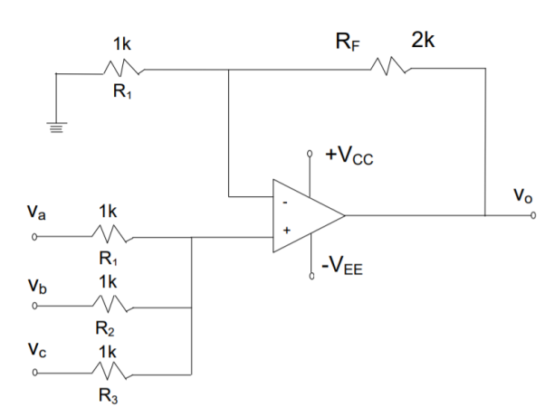
A6)
In the amplifier circuit shown in fig. Since the resistors R1, R2, and R3 are all equal to 1kΩ, the voltage V1, at non-inverting input terminal will be average of the three voltages, Va, Vb, and Vc. Thus,


And the gain for non-inverting amplifier, AV, is


Q7) Differential gain Ad, of an op amp measures 100. In the measurement of common mode gain experiment when 1.0V is applied common to both the inputs, output voltage measured is 0.01V. How much is common-mode rejection ratio (CMRR)?
A7)
By definition, common mode rejection ratio (CMRR) is

Where Ad is gain in differential mode which is given as 100.
And, the gain in common mode, ACM is,

Therefore,


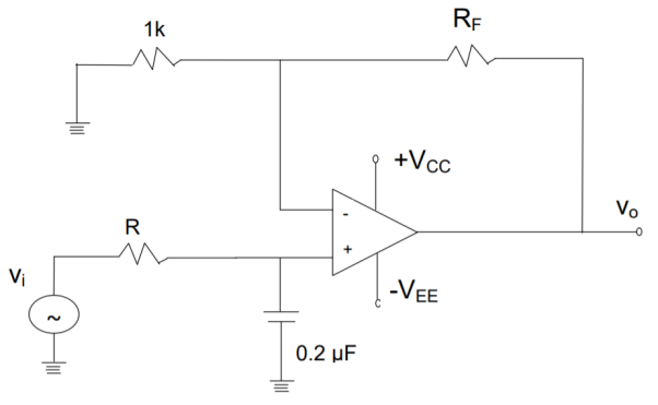
Q8) Figure shows a low-pass filter. Calculate the value of feedback resistor RF so that band-pass gain is 100. Also calculate the value of resistor R to get cut-off frequency of 2kHZ.
A8)
The gain in band-pass region is that of non-inverting amplifier and it is,

 then
then


The cut-off frequency, f, for low-pass fitter is given by


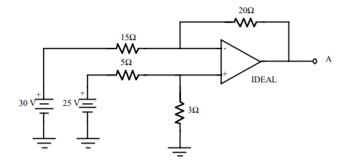
Q9) For the difference amplifier circuit shown, determine the output voltage at terminal A.
A9)
By voltage division,

By the virtual short circuit between the input terminals, vin- = 9.375 V Using Ohm's law, the current through the 15 Ω resistor is

The input impedance is infinite; therefore, Iin-=0 and I15=I20. Use Kirchoff's voltage law to find the
Output voltage at A.

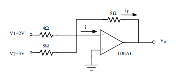
Q10) What is the current, i?
A10)
The input current of IDEAL op amp is very small. Hence, it is considered to be 0. So, i=0A
Q11) What is the output voltage, vo? For circuit shown in Q10).
A11)
This op amp circuit is a summing amplifier. Since i=0,

 )(8
)(8
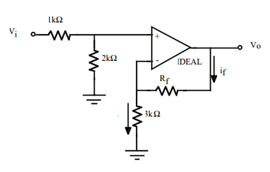
Q12) For the ideal op amp shown, what should be the value of resistor Rf to obtain a gain of 5?
A12)
By voltage division

By the virtual short circuit


Since the op amp draws no current, if=i

But, vo = 5vi.


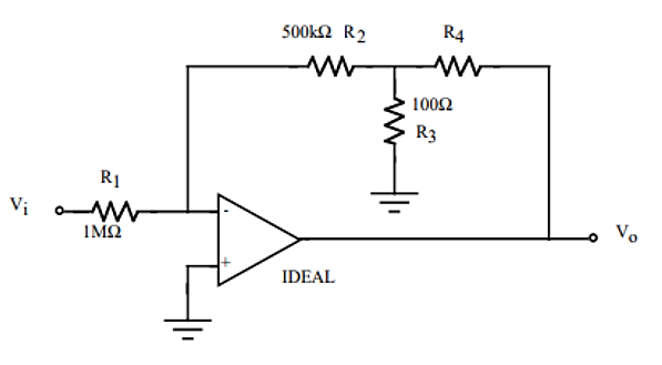
Q13) Evaluate the following amplifier circuit to determine the value of resistor R4 in order to obtain a voltage gain (vo/vi) of -120
A13)

vin+ is grounded, so vin- is also a virtual ground.
vin- = 0
Since vin- = 0, vi=i1Rl and il=vi/R1.
Since vin- = 0, vx=-i2R2 and i2=-vx/R2.
Similarly, vx=-i3R3
vx-vo =-i4R4
From Kirchhoff's current law, i4 = i2 + i3

Now, vo=-120vi.
Also, il=i2, so


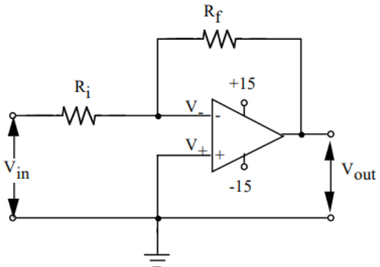
Q14) For the circuit shown below If Rf = 1MW and Ri=50W, what is the voltage gain?

A14)
There are two ways to solve any problem involving an op amp. The first way is to use

Where va is the input to the inverting terminal and vb is the input to the non-inverting terminal. In this case, there is no input to the non-inverting input and vb=0. The formula reduces to the simple result

Using the given circuit values, we get

The voltage gain is then -20,000. Note that any value over 100 is impractical for any real amplifier. A more general way of solving any op amp circuit is to note that an ideal (and most real) op amps must satisfy the virtual short assumption, i.e. that V+=V-. Using this assumption and KCL at an input node is adequate to solve most any op amp problem. In this case, KCL at the inverting input gives


So, we get the same result. Note that any value over 100 is impractical for any real amplifier
Q15) For the circuit shown below, If Vin=0.1 volts, what is Vout?
A15)
Solve same as above question We get vo = – 20,000vin = – 20,000 (0.1 volts) = – 2000 volts As mentioned previously, this is a ridiculous value for an output.
Q16) For the circuit shown below, V1 = 10sin 200t and V2 = 15sin 200t. What is Vout? The op amp is ideal with infinite gain.

A16)
Any problem with a capacitor (or inductor) in it and sinusoidal voltages immediately indicates that phasors are required. This means that V1 and V2 should be represented as phasors, and Cf should be replaced by an impedance. This problem is not solved very well with the formulas in the Reference Handbook. This circuit is most easily solved using the virtual short assumption (V+=V-), and using KCL at the inverting input. Note that the grounding of V+ then requires that V-=0. This is also called the virtual short assumption.

Rationalizing this expression gives

Solving for Vout gives

It is important to recognize that all sine functions should always be converted to cosines for proper phase in the phasor expressions, i.e. sin 200t = cos (200t – 90)0 ´ 1- 90 = –j
Using the circuit parameters given,


The answer is then

Q17) Explain frequency response of IC 741?
A17)
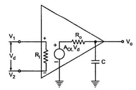
Fig 1 High frequency model of OP-AMP
- Frequency response of the op-amp is the plot of its open loop gain versus frequency.
- The open loop gain changes with frequency.
- To plot the frequency response, we need to refer high frequency model of OP-AMP.
- After a certain frequency the roll-off decreases after certain frequency.
- The capacitor is due to BJT used in the 741.
- The BJTs has parasitic capacitances so the capacitances is too small.
- So, in order to reduces the effect of this parasitic capacitances the compensated capacitor is used in 741.

Fig 2 Frequency Response
Q18) Derive the expression showing relation between ft and slew rate?
A18)
Relationship between ft and SR can be found by

As we know that

So, 
So,

And we get

Finally, we get, 