Unit - 2
Applications of 8051 Microcontroller
Q1) Write the program for interfacing LED with 8051?
A1)
LED is connected to AT89C51 microcontroller with the current limiting resistor. The value of this resistor is calculated using the following formula.
R= (V-1.7)/10mA, where V is the input voltage.
The maximum output voltage of microcontrollers is 5V. Hence the calculated value of resistor is 330 Ohms. The resistor can be connected to cathode or the anode of LED.
- Initially, burn the code into the microcontroller.
- Connect the LEDs to the Port0 of the microcontroller.
- Switch on the circuit.
- The LEDs start glowing.
- Switch off the circuit.
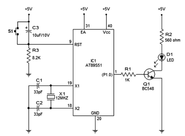
Figure 1. LED Interfacing
- In the circuit, push button switch S1, capacitor C3 and resistor R3 forms the reset circuitry.
- When S1 is pressed, voltage at the reset pin (pin9) goes high and this resets the chip. C1, C2 and X1 are related to the on -chip oscillator to produces the required clock frequency.
- P1.0 (pin1) is acts as the output pin. When P1.0turns high transistor Q1 is forward biased and LED gets ON. When P1.0 turns low, the transistor gets cut off and the LED extinguishes.
- The transistor driver circuit for the LED can be avoided and the LED can be connected directly to the P1.0 pin along with the series current limiting resistor(~1K).
- The time for which P1.0turns high and low (time period of the LED) is determined by the program.
Program:
START: CPL P1.0
ACALL WAIT
SJMP START
WAIT: MOV R4,#05H
WAIT1: MOV R3,#00H
WAIT2: MOV R2,#00H
WAIT3: DJNZ R2,WAIT3
DJNZ R3,WAIT2
DJNZ R4,WAIT1
RET
Q2) Write a C program for the 8051 to transfer the letter "A" serially at 4800 baud continuously. Use 8-bIt data and 1 stop bit.
A2)
#include <regSl.h>
Void main(void)
{
TMOD=Ox20; //use Timer 1,8-BIT auto-reload
TH1=OXFA; //4800 baUd rate
SCON=OxSO;
TR1=l;
While(l)
{
SBUF=' A'; //place value in buffer
While (TI==O);
TI=O;
}
}
Q3) Write an 8051 C program to transfer the message "YES" serially at 9600 baud 8-bit data, 1 stop bit, Do this continuously.
A3)
#include <regSl.h>
Void SerTx(unsigned char);
Void main (void)
{
TMOD=Ox20; //use Timer 1,8-BIT auto-reload
THl=OxFD; //9600 baUd rate
SCON=OxSO; //start timer
TRl=l;
While(l)
{
SerTx('Y');
SerTx (,E ');
SerTx (,S ');
}
}
Void SerTx(unsigned char x)
{
SBUF=x; //place value in buffer
While (TI==O); //wait until transmitted
TI=O;
}
Q4) Program the 8051 in C to receive bytes of data serially and put them in Pl. Set the baud rate at 4800, 8-bit data, and I stop bit.
A4)
#include <regSl.h>
Void main (void)
{
Unsigned char mybyte; //use Timer 1,8-BIT auto-reload
TMOD=Ox20; //4800 baud rate
THl=OxFA;
SCON=OxSO;
TRl=l; //start timer
While (1) //repeat forever
{
,
While (RI==O); //wait to receive
Mybyte=SBUF; //save value
Pl=mybyte; //write value to port
RI=O;
}
}
Q5) Write an 8051 C program to send two different strings to the serial port. Assuming that SW is connected to pin P2.0, monitor its status and make a decision as follows:
SW = 0: send your first name
SW = I: send your last name
Assume XTAL= 11.0592MHz, baud rate of 9600, 8-bit data, I stop bit.
A5)
#include <reg51.h>
Sbit MYSW=P2AO; //input switch
Void main (void)
{
Unsigned char z,
Unsigned char fname []="ALI";
Unsigned char lname []="SMITH";
TMOD=Ox20; //use Timer l, a-BIT auto-reload
THl=OxFD; //9600 baud rate
SCON=Ox50;
TRI=l; //start timer
If (MYSW==O) //check switch
{
For(z=O;z<3;z++) //write name
{
SBUF=fname[z]; //place value in buffer
While (TI==O) ; //wait for transmit
TI=O;
}
}
Else
{
For(z=o;z<s;z++) //write name
{
SBUF=lname[z]; //place value in buffer
While (TI==O); //wait for transmit
TI=O;
}
}
}
Q6) Write an 8051 C program to send the two messages "Normal Speed" and "High Speed" to the serial port. Assuming that SW is connected to pin P2.0, monitor its status and set the baud rate as follows:
SW = 0 28,800 baud rate,
SW = 1 56K baud rate
Assume that XTAL = 11.0592 MHz for both cases.
A6)
#include <reg51.h>
Sbit MYSW=P2AO; //input switch
Void main(void)
{
Unsigned char. Z;
Unsigned char Messl []= "Normal Speed";
Unsigned char Mess2 [] ="High Speed";
TMOD=Ox20; //use Timer 1,8-BIT auto-reload
THI=OxFF; //28,800 for normal speed
SCON=Ox50;
TRl=l; //start timer
If (MYSW==O)
{
For(z=0;z<12;z++)
{
SBUF=Messl[z]; //place value in buffer
While (TI==O); //wait for transmit
TI=O;
}
}
Else
{
PCON=PCONIOx80;// for high speed of 56K
For(z=O;z<IO;z++)
{
SBUF=Mess2[z]; //place value in buffer
While (TI==O); //wait for transmit
TI=O;
}
}
}
Q7) Write a C program for the DS89C4xO to transfer letter "A" serially at 4800 baud continuously. Use the second serial port with 8-bit data and I stop bit. We can only use Timer 1 to set the baud rate.
A7)
#include <regsl.h>
Sfr SBUFhOxCl;
Sfr SCON1=OxCO;
Sbi t TIl=OXC1;
Void main (void)
(
TMOD=Ox20; //use Timer 1 for 2nd serial port
TH1=OxFA; //4800 baud rate
SCON1=OxSO; //use 2nd serial port SCONl register
TR1=1; //start timer
While (l)
{
SBUFl='A';//us~ 2nd serial port SBUFl register
While (TI1~=O); //walt for transmit
TI1=O;
}
}
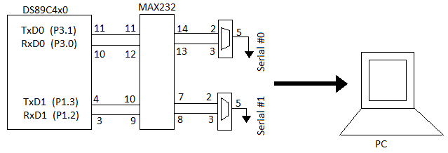
Q8) Program the DS89C4xO in C to receive bytes of data serially via the serial port and put them in P1. Set the baud rate at 9600, 8-bit data and 1-stop bit. Use Timer 1 for baud rate generation.
A8)
#include <regS1.h>
Sfr SBUF1=OxC1'
Sfr SCON1=OXCO:
Sbit RI1=OxCO" ,
Void main (void)
{
Unsigned char mybyte;
TMOD=0x20; //use Timer1,8-BIT auto-reload
TH1=0xFD;//9600
SCON1=0xS0;//use SCON1 of 2nd serial port
TR1=1;
While (1)
{
While (RIl==O);//monitor RI1 of 2nd serial port
Mybyte=SBUF1'; //use SBUF1 of 2nd serial port
P2=mybyte; //place value on port
RIl=O;
}
}
Q9) Write a program to interface data acquisition system with 8051?
A9)
Start: MOV P1, #00H
LCALL initserial
LCALL latch
LCALL start_conv
LCALL wait
LCALL get
MOV A,P2
MOV R6,A
LCALL send_read
SJMP start
Delay: MOV R4,#80H
Here: MOV R5,#30H
Again: DJNZ R5,again
DJNZ R4,here
RET
Initserial: MOV TMOD,#20H
MOV TH1,#FDH
MOV SCON,#50H
SETB TR1
SETB EA
SETB ES
RET
Start_conv: LCALL delay
CLR P3.3
LCALL delay
SETB P3.3
RET
Wait: JB P3.4,wait
RET
Get: LCALL delay
CLR P3.5
LCALL delay
SETB P3.5
RET
Send_char: MOV SBUF,R6
Next: JNB TI,next
CLR TI
RET
Send_read: LCALL send_char
MOV A,#”.”
LCALL send_char
RET
Latch: CLR P3.6
LCALL delay
SETB P3.6
RET
Q10) Write a program for interfacing opto-isolator with 8051?
A10)
ORG 00H
MOV P3,#00H;Configure PORT3 as output
Again:setb P3.5 ;relay ON,Buzzer ON
Acall Delay
Clr P3.5;relay Off,Buzzer off
Acall Delay
Sjmp again
Delay:Mov R3,#08H
Up2:Mov R2,#0FFH
Up1:Mov R1,#0FFHH
Here:DJNZ R1,
Here: DJNZ R2,
Up1
DJNZ R3,Up2
RET
END
Q11) Draw the circuit diagram for interfacing a buzzer with 8051. Also write the program for interfacing?
A11)
Buzzer is an electronic device that converts the electronic signal into buzzing noise, that is applied to it.
Interfacing:
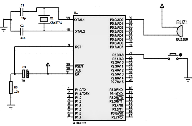
Figure 2. Interfacing with buzzer
Pin 40 and 31 is connected to Vcc(5v). Port 1.5 is connected with an inverter and then to the buzzer. Pin 18 and 19 are connected to a crystal oscillator with ceramic 0.01uf capacitor. The buzzer gets turned on when port 2.3 is high.
For resetting the buzzer pin 31 and 3 are connected together with 1uf capacitor and then connected to ground through 10K resistor.
Program:
Org 00H
HERE: JNB P2.3,HERE ;keep monitoring for high
SET B P1.5 ;set bit P1.5
CLR P1.5 ;make P1.5 low
SJMP HERE ; keep repeating
END
Q12) Write the code for interfacing relay with 8051?
A12)
Relay equ P0.0
Swequ P1.0
;*************************************************
Org 0000h
Main:clr relay ;Configure inp and outp
Setb sw
Up: jnbsw,on ;wait for switch to be pressed
Clr relay
Acall delay
Sjmp up
On: setb relay ;Turn ON relay
Acall delay
Acall delay
Here:jb sw,here ;wait for switch to be released
Clr relay ;Turn OFF relay
Acall delay
Acall delay
Sjmp up ;Loop
;*************************************************
Delay:mov r7,#0ffh ;delay subroutine
Again:mov r6,#0ffh
Djnz r6,$
Djnz r7,again
Ret
;*************************************************
End
Q13) WAP for Interfacing Stepper Motor with 8051?
A13)
Main: MOV A, # 0FF H ; Initialization of Port 1
MOV P1, A ;
MOV A, #77 H ; Code for the Phase 1
MOV P1, A ; ACALL DELAY ; Delay subroutine
MOV A, # BB H ; Code for the Phase II
MOV P1, A ;
ACALL DELAY ; Delay subroutine.
MOV A, # DD H ; Code for the Phase III
MOV P1, A ; ACALL DELAY ;
MOV A, # EE H ; Code for the Phase 1
MOV P1, A ;
ACALL DELAY ; Delay subroutine
SJMP MAIN; Keep the motor rotating continuously.
DELAY Subroutine
MOV R4, #0FF H ; Load R4 with FF
MOV R5, # 0FF ; Load R5 with FF
LOOP1: DJNZ R4, LOOP1 ; Decrement R4 until zero,wait
LOOP2: DJNZ R5, LOOP2 ; Decrement R5 until zero,wait
RET ; Return to main program .
Q14) WAP for Interfacing 8051 with ADC0808?
A14)
SOC EQU P2.6
EOC EQU P2.5
OE EQU P2.4
ALE EQU P2.3
ADDR_C EQU P2.2
ADDR_B EQU P2.1
ADDR_A EQU P2.0
ORG 0000H
MOV P1, #0FFH
SETB P2.5
CLR SOC
CLR OE
CLR ALE
AGAIN: CLR ADDR_C
CLR ADDR_B
CLR ADDR_A
SETB SOC
SET ALE
ACALL DELAY
CLR SOC
CLR ALE
BACK: JB EOC BACK
HERE: JNB EOC HERE
SETB OE
MOV A,P1
ACALL CONVERSION
ACALL DISPLAY
AGAIN: SJMP AGAIN
Q15) WAP for Interfacing 8051 with DAC 0808 for generation of square wave, triangular wave and stair wave?
A15)
ORG 000H
MOV P1, #00H
Call squarwave
Call triwave
Call stairwave
Jmp repeat
Squarwave: MOV P1,#FFH
Call delay2sec
MOV P1,#00H
Call delay2sec
Ret
Triwave: MOV R7,#00H
Triwave1: MOV P1,R7
Inc R7
Cjne R7, #FFH, triwave1
MOV R7, #FFh
Triwave2: MOV P1, R7
Djnz R7, triwave2
RET
Stairwave: MOV P1, #00H
Call delay2sec
MOV P1, #20H
Call delay2sec
MOV P1, #40H
Call delay2sec
RET
Delay1sec: MOV R0,#10
Del2 : MOV R1,#250
Del1: MOV R2,#250
DJNZ R2,$
DJNZ R1,del2
DJNZ R0,del1
RET
Delay2sec: MOV R0,#20
Del2 : MOV R1,#250
Del1: MOV R2,#250
DJNZ R2,$
DJNZ R1,del21
DJNZ R0,del22
RET
END
Q16) Write a program for Seven Segment Display Interfacing with 8051?
A16)
Start of main program:
To check that whether any key is pressed
Start: mov a,#00h
Mov p1,a; making all rows of port p1 zero
Mov a,#0fh
Mov p1,a; making all rows of port p1 high
Press:mov a,p2
Jz press; check until any key is pressed
After making sure that any key is pressed
Mov a,#01h; make one row high at a time
Mov r4,a
Mov r3,#00h; initiating counter
Next: mov a,r4
Mov p1,a; making one row high at a time
Mov a,p2; taking input from port A
Jnzcolscan; after getting the row jump to check column
Mov a,r4
Rl a; rotate left to check next row
Mov r4,a
Mov a,r3
Add a,#08h; increment counter by 08 count
Mov r3,a
Sjmp next; jump to check next row
After identifying the row to check the colomn following steps are followed
Colscan: mov r5,#00h
In: rrc a; rotate right with carry until get the carry
Jc out; jump on getting carry
Inc r3; increment one count
Jmp in
Out: mov a,r3
Da a; decimal adjust the contents of counter
Before display
Mov p2,a
Jmp start; repeat for check next key.
Q17) Write a program to interface keypad with 8051?
A17)
#include<reg51.h>
#define display_port P2 //Data pins connected to port 2 on microcontroller
Sbit rs = P3^2; //RS pin connected to pin 2 of port 3
Sbit rw = P3^3; // RW pin connected to pin 3 of port 3
Sbit e = P3^4; //E pin connected to pin 4 of port 3
Sbit C4 = P1^0; // Connecting keypad to Port 1
Sbit C3 = P1^1;
Sbit C2 = P1^2;
Sbit C1 = P1^3;
Sbit R4 = P1^4;
Sbit R3 = P1^5;
Sbit R2 = P1^6;
Sbit R1 = P1^7;
Void msdelay(unsigned int time) // Function for creating delay in milliseconds.
{
Unsigned i,j ;
For(i=0;i<time;i++)
For(j=0;j<1275;j++);
}
Void lcd_cmd(unsigned char command) //Function to send command instruction
To LCD
{
Display_port = command;
Rs= 0;
Rw=0;
e=1;
Msdelay(1);
e=0;
}
Void lcd_data(unsigned char disp_data) //Function to send display data to LCD
{
display_port = disp_data;
rs= 1;
rw=0;
e=1;
msdelay(1);
e=0;
}
Void lcd_init() //Function to prepare the LCD and get it ready
{
lcd_cmd(0x38); // for using 2 lines and 5X7 matrix of LCD
msdelay(10);
lcd_cmd(0x0F); // turn display ON, cursor blinking
msdelay(10);
lcd_cmd(0x01); //clear screen
msdelay(10);
lcd_cmd(0x81); // bring cursor to position 1 of line 1
msdelay(10);
}
Void row_finder1() //Function for finding the row for column 1
{
R1=R2=R3=R4=1;
C1=C2=C3=C4=0;
If(R1==0)
lcd_data('1');
if(R2==0)
lcd_data('4');
if(R3==0)
lcd_data('7');
if(R4==0)
lcd_data('*');
}
Void row_finder2() //Function for finding the row for column 2
{
R1=R2=R3=R4=1;
C1=C2=C3=C4=0;
If(R1==0)
lcd_data('2');
if(R2==0)
lcd_data('5');
if(R3==0)
lcd_data('8');
if(R4==0)
lcd_data('0');
}
Void row_finder3() //Function for finding the row for column 3
{
R1=R2=R3=R4=1;
C1=C2=C3=C4=0;
If(R1==0)
lcd_data('3');
if(R2==0)
lcd_data('6');
if(R3==0)
lcd_data('9');
if(R4==0)
lcd_data('#');
}
Void row_finder4() //Function for finding the row for column 4
{
R1=R2=R3=R4=1;
C1=C2=C3=C4=0;
If(R1==0)
lcd_data('A');
if(R2==0)
lcd_data('B');
if(R3==0)
lcd_data('C');
if(R4==0)
lcd_data('D');
}
Void main()
{
lcd_init();
while(1)
{
msdelay(30);
C1=C2=C3=C4=1;
R1=R2=R3=R4=0;
if(C1==0)
row_finder1();
else if(C2==0)
row_finder2();
else if(C3==0)
row_finder3();
else if(C4==0)
row_finder4();
}
}
Q18) How many IO ports are present in 8051 explain all of them?
A18)
The 8051 has four 8-bit I/O ports: P0, P1, P2, and P3. We can access either the entire 8 bits or any single bit without altering the rest. When accessing a port in a single-bit manner, we usc the syntax "SETB X. y" where X is the port number 0, 1,2, or 3, and Y is the desired bit number from 0 to 7 for data bits D0 to 07. See Figure 5-2. For example, "SETB Pl. 5" sets high bit 5 of port 1. Remember that D0 is the LSB and D7 is the MSB.
Every SFR register is assigned a byte address and ports PO - P3 are part of the SFR. For example, PO is assigned byte address 80H, and PI has address of 90H as shown in Figure below. While all of the SFR registers are byte-addressable some of them are also bit-addressable. The P0- P3 are among this category of SFR registers. From Figure below we see that the bit addresses for P0 are 80H to 87H, and for P I arc 90H to 97H, and so on.
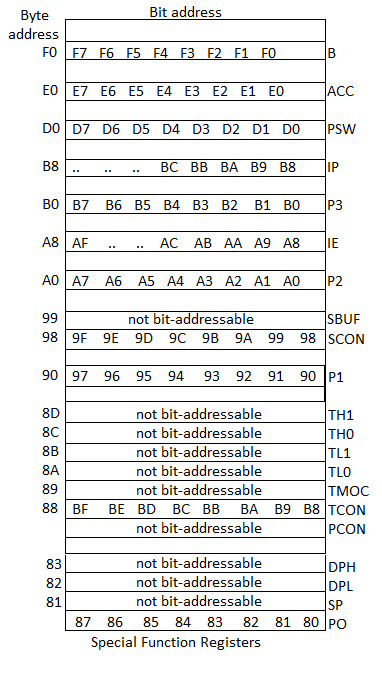
Fig 3. SFR RAM address
When code such as "SETB Pl.0" is assembled, it becomes "SETB 90H"since P 1.0 has the RAM
Address of 90H. The bit addresses 00 - 7FH belong to RAM byte addresses 20 - 2FH, and bit addresses 80 - F7H belong to SFR of P0, TCON, P1, SCON, P2, etc. The bit addresses for P0 - P3 are below
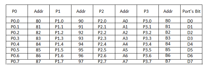
Fig 4. Bit address of all ports
Q19) Draw the pin diagram for 8051 and mention function of the respective pins?
A19)
The pin diagram of 8051 microcontroller consists of 40 pins as shown below. A total of 32 pins are set away into four Ports such as P0, P1, P2 and P3. Where, each port contains 8 pins. Therefore, the microcontroller 8051 pin diagram and explanation are given below.
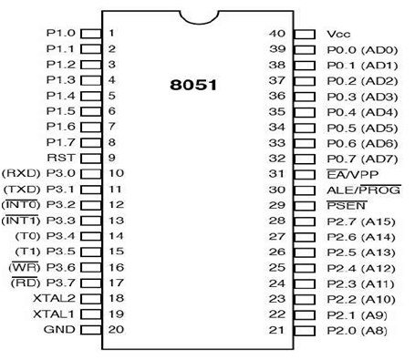
Figure 5 PIN Diagram of 8051
- Port1 (Pin1 to Pin8): Port1 includes pin1.0 to pin1.7 and these pins can be configured as input or output pins.
- Pin 9 (RST): Reset pin is used to Reset 8051 Microcontroller by giving a positive pulse to this Pin.
- Port3 (Pin 10 to 17): The Port3 Pins are similar to port1 pins and can be used as universal Input or output pins. These pins dual-function Pins and the function of each Pin is given as:
- Pin 10 (RXD): RXD pin is a Serial Asynchronous Communication Input or Serial synchronous Communication Output.
- Pin 11 (TXD): Serial Asynchronous Communication Output or Serial Synchronous Communication clock Output.
- Pin 12 (INT0): Input of Interrupt 0
- Pin 13 (INT1): Input of Interrupt 1
- Pin 14 (T0): Input of Counter 0 clock
- Pin 15 (T1): Input of Counter 1 clock
- Pin 16 (WR): Writing Signal to write content on external RAM.
- Pin 17 (RD): Reading Signal to read contents of external RAM.
- Pin 18 and 19 (XTAL2, XTAL1): X2 and X1 pins are input output pins for the oscillator. These pins are used to connect an internal oscillator to the microcontroller.
- Pin 20 (GND): Pin 20 is a ground pin.
- Port2 (Pin 21 to Pin28): Port2 includes pin21 to pin28 which can be configured as Input Output Pins. But, this is only possible when we don’t use any external memory. If we use external memory, then these pins will work as high order address bus (A8 to A15).
- Pin 29 (PSEN): This pin is used to enable external program memory. If we use an external ROM for storing the program, then logic 0 appears on it, which indicates Micro controller to read data from the memory.
- Pin 30 (ALE): Address Latch Enable pin is an active high-output signal. If we use multiple memory chips, then this pin is used to distinguish between them. This Pin also gives program pulse input during programming of EPROM.
- Pin 31 (EA): If we have to use multiple memories then the application of logic 1 to this pin instructs the Microcontroller to read data from both memories: first internal and then external.
- Port 0 (Pin 32 to 39): Similar to the port 2 and 3 pins, these pins can be used as input output pins when we don’t use any external memory. When ALE or Pin 30 is at 1, then this port is used as data bus: when the ALE pin is at 0, then this port is used as a lower order address bus (A0 to A7)
- Pin40 (VCC): This VCC pin is used for power supply.
Q20) With the help of circuit diagram explain the interfacing of keypad?
A20)
There are set of PUSH buttons in matrix keypads which are interconnected. For 4x4 matrix there are 4 PUSH buttons in each of the 4 rows. One terminal of all 4 PUSH buttons is connected in row 1. The other terminal represents the 4 columns. Hence, there are 8 terminals we need to connect with a microcontroller.
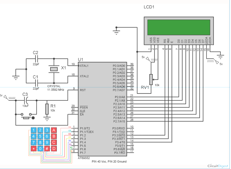
Fig 6 Interfacing of Keypad
Before interfacing keypad, it is important to interface LCD with the microcontroller. The 8 terminals of the keypads need to be connected to any of the 8 pins (ports) of the microcontroller. We need to know the number of row and column whenever any button is pressed. After tracking location we can print the character accordingly.
Now the question is how to get the location of the pressed button. This is explained below:
1. First we have made all the Rows to Logic level 0 and all the columns to Logic level 1.
2. Whenever we press a button, column and row corresponding to that button gets shorted and makes the corresponding column to logic level 0. Because that column becomes connected (shorted) to the row, which is at Logic level 0. So we get the column no. See main() function

Figure 7 Finding Column Number
3. Now we need to find the Row no., so we have created four functions corresponding to each column. Like if any button of column one is pressed, we call function row_finder1(), to find the row no.
4. In row_finder1() function, we reversed the logic levels, means now all the Rows are 1 and columns are 0. Now Row of the pressed button should be 0 because it has become connected (shorted) to the column whose button is pressed, and all the columns are at 0 logic. So, we have scanned all rows for 0.

Fig 8 Finding Row number
5. So whenever we find the Row at logic 0, means that is the row of pressed button. So now we have column no (got in step 2) and row no., and we can print no. Of that button using lcd_data function.