Unit - 4
Introduction to other advanced microcontrollers
Q1) Explain features of ARM and PIC processor?
A1)
- An ARM processor is one of a family of CPUs based on the RISC (reduced instruction set computer) architecture developed by Advanced RISC Machines (ARM).
- ARM processors are extensively used in consumer electronic devices such as smart phones, tablets, multimedia players and other mobile devices, such as wearables.
Features
- This has high performance RISC CPU.
- 40-pin PDIP, high performance, enhanced Flash Microcontroller with CAN.
- The Operating speed ranges between 40 MHz up to 10 MIPS.
- The Operating voltage ranges 4.2 to 5.5 V
- ROM of size 2M bytes
- RAM between 256 bytes to 4096 bytes.
- On-chip program ROM in form of flash memory.
- Data EEPROM
- 8 x 8 Single cycle Hardware Multiplier
- 16-bit wide instructions, 8-bit wide data path.
- 75 instructions.
- ADC and USART PROTOCOL for PC communication.
- I/O port between 16 to 72 pins and I/O port register are bit and port accessible.
- SPI PROTOCOL and I2C PROTOCOL for memory communication.
- PIC 18F458 has two-stage pipeline.
- Interrupt capability with Priority levels.
- Linear program memory addressing upto 2 Mbytes
Selection:
- Speed
- Amount of RAM/ROM
- Numbers of I/O pins, Timers
- Power Consumption
- Tools of availability
- Added features like ADC/DAC/CCP, Bus support like CAN, SPI, I2C, USB.
- Watch Dog timer, Timer modes, Data EEPROM.
ARM Processors
ARM Processors can be divided into
- ARM Classic Processors: Arm classic processors include the Arm11, Arm9, and Arm7 processor families. These processors are still widely used around the globe, providing cost-effective solutions for many of today's applications.
- ARM Embedded Processors: Software development for embedded applications includes anything which uses a microcontroller or microprocessor to execute dedicated tasks on its own or within a larger system. Arm supports embedded software development at every stage of the project workflow.
- ARM Application Processors: Advanced RISC machine (ARM) is the first reduced instruction set computer RISC processor for commercial use, which is currently being developed by ARM holdings. ... ARM processor finds applications in digital TVs, set-top boxes, smart phones, mobile, laptops etc.
- ARM Classic processors include ARM7, ARM9 and ARM11 families and ARM7TMDI is still the highest shipping 32-bit processor. ARM7 based processors are still used in many small and simple 32-bit devices.
Version ARM 7:
- ARM7 is a group of older 32-bit RISC ARM processor cores licensed by ARM Holdings for microcontroller use.
- The ARM7 core family consists of ARM700, ARM710, ARM7DI, ARM710a, ARM720T, ARM740T, ARM710T, ARM7TDMI, ARM7TDMI-S, ARM7EJ-S. The ARM7TDMI and ARM7TDMI-S were the most popular cores of the family.
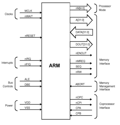
Fig. ARM7 FUNCTIONAL DIAGRAM
- The final thing that must be explained is how the ARM will be used and the way in which the chip appear.
- The various signals that interface with the processor are input, output or supervisory signals which will be used to control the ARM operation.
PIC
- This has high performance RISC CPU.
- 40-pin PDIP, high performance, enhanced Flash Microcontroller with CAN.
- The Operating speed ranges between 40 MHz up to 10 MIPS.
- The Operating voltage ranges 4.2 to 5.5 V
- ROM of size 2M bytes
- RAM between 256 bytes to 4096 bytes.
- On-chip program ROM in form of flash memory.
- Data EEPROM
- 8 x 8 Single cycle Hardware Multiplier
- 16-bit wide instructions, 8-bit wide data path.
- 75 instructions.
- ADC and USART PROTOCOL for PC communication.
- I/O port between 16 to 72 pins and I/O port register are bit and port accessible.
- SPI PROTOCOL and I2C PROTOCOL for memory communication.
- PIC 18F458 has two-stage pipeline.
- Interrupt capability with Priority levels.
- Linear program memory addressing upto 2 Mbytes
Q2) Explain the architecture of PIC microcontroller?
A2)
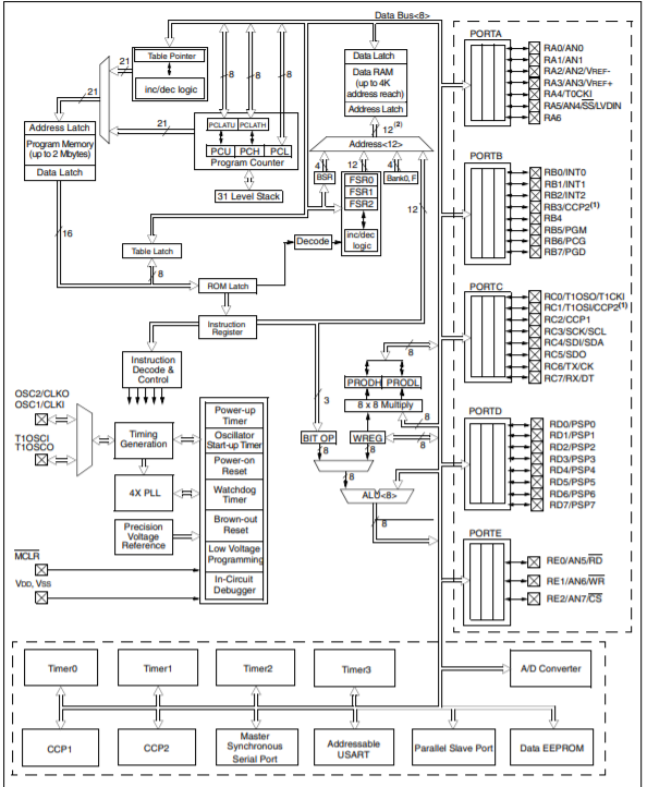
Figure 1. Architecture of PIC controller
The microcontroller architecture consists of CPU, I/O ports, memory organization, A/D converter, timers/counters, interrupts, serial communication, oscillator and CCP module
CPU (Central Processing Unit)
The PIC microcontroller CPU consists of the Arithmetic and Logic Unit, Memory Unit, Control Unit, accumulator and so on.
Arithmetic logic unit are mainly used for arithmetic operations and logical decisions. After processing, for storing the instructions memory is used. To control the internal and external peripherals, control unit is used to connect to CPU and accumulator is used for storing results.
Memory Organization
The memory module consists of RAM, ROM and STACK.
Random Access Memory (RAM)
RAM is an unstable memory used to store data temporarily in its registers. The registers of RAM are classified into Special Function Registers (SFR) and General-Purpose Registers (GPR).
- General Purpose Registers (GPR)
These registers are used for general purpose only.
- Special Function Registers
They are mainly used for special purposes only. These registers perform according to the functions assigned to them,
The STATUS register cannot be used for storing data, these registers are used for showing the operation or status of the program.
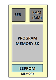
Figure. Memory Organization
Read Only Memory (ROM)
Read only memory is a stable memory used to store the data permanently. In PIC microcontroller ROM stores the instructions or programs. The microcontroller acts according to the program.
The ROM is also called as program memory, here the user writes the program and saves it permanently and executed by CPU. The microcontroller’s performance depends on the instruction executed by the CPU.
Electrically Erasable Programmable Read Only Memory (EEPROM)
Normally in ROM, we write the program only once and cannot use it multiple times. But, in EEPROM you can program the ROM multiple times.
Flash Memory
Flash memory also known as programmable read only memory (PROM) can read, write and erase the program thousands of times. PIC microcontroller uses this type of ROM.
Stack
When an interrupt occurs, first the PIC microcontroller must execute the interrupt and the existing process address that is being executed and store it in the stack. After completing the execution of the interrupt, the microcontroller calls the process with the help of address, which is stored in the stack and executes the process.
BUS
BUS is used for transfer and receive of data from one peripheral to another. It is classified into two types that is address and data bus.
Data Bus: It is used to transfer or receive the data.
Address Bus: Address bus transmits the memory address from peripherals to CPU. I/O pins are used to interface with external peripheral. UART and USART are serial communication protocols used for interfacing serial devices like GSM, GPS, Bluetooth, IR, and so on.
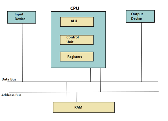
Figure. BUS
A/D converters
The analog to digital converter converts analog voltage values to digital voltage values. A/D module of PIC microcontroller consists of 5 inputs of 28 pin devices and 8 inputs of 40 pin devices.
The operation of the analog to digital converter is controlled by special registers ADCON0 and ADCON1. The upper bits of the converter are stored in ADRESH register and lower bits of the converter are stored in ADRESL register. It requires 5V of an analog reference voltage for operation.
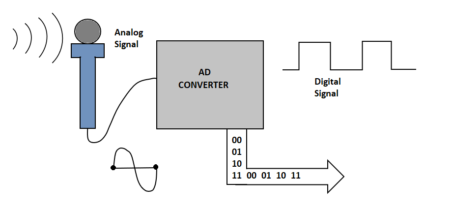
Figure. A/D CONVERTER
Timers/ Counters
PIC microcontroller consists of four timer/counters wherein one is 8-bit timer and the remaining timers can be 8 or 16-bit mode. Timers are used for generating accuracy actions, for example, creating specific time delays between two operations.
Interrupts
PIC microcontroller consists of 20 internal interrupts and three external interrupt sources associated with different peripherals like ADC, USART, Timers, and so on.
Serial Communication
Serial communication is the method used for transferring data one bit at a time sequentially over communication channel.
- USART: (Universal synchronous and Asynchronous Receiver and Transmitter)
The two serial communication protocols used for transmitting and receiving data bit by bit over a single wire with respect to clock pulses. The PIC microcontroller has two pins TXD and RXD used for transmitting and receiving the data serially.
- SPI Protocol: (Serial Peripheral Interface)
This protocol is used for sending data between PIC microcontroller and other peripherals which include SD cards, sensors and shift registers.
PIC microcontroller supports three- wire SPI communications between two devices on a common clock source.
- I2C Protocol: (Inter Integrated circuit)
A serial protocol used to connect low speed devices such as EEPROMS, microcontrollers, A/D converters, and so on. PIC microcontroller support two wire Interface or I2C communication between two devices which can work as Master and Slave device.
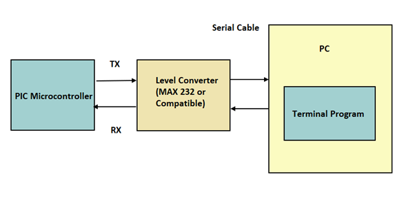
Figure. Serial Communication
CCP module
CCP module stands for capture/compare/PWM.
- Capture Mode: Capture mode captures the time of arrival of a signal, that is when the CCP pin goes high, it captures the value of Timer1.
- Compare Mode: Compare mode acts as analog comparator. When timer1 value reaches certain reference valueit generates output.
- PWM Mode: PWM mode provides pulse width modulated output with 10-bit resolution and programmable duty cycle.
Q3) List characteristics of 16-bit microcontroller?
A3)
Characteristics if 16 bit characteristics
CPU16
1. 16 Bit Architecture
2. Control-Oriented Digital Signal Processing Capability
3. 16 bit Multiply and Accumulate (digital signal processing)
4. 1 Megabyte of Program Memory Space and 1 Megabyte of Data Memory Space
5. High Level Language Support
6.Fast Interrupt Response Time
7. Hardware Breakpoint Signal
8. Background Debugging Mode (BDM)
9. Fully Static Operation
10. Watchdog Timer, Clock Monitor and Bus Monitor
11. Parallel Ports Option on Address and Data Bus in Single Chip Mode
12. Two 8 bit Dual Function Input/Output Ports
13. One 7 bit Dual Function Output Port
14. Phase-Locked Loop (PLL) Clock System
15. Multichannel Communication Interface (MCCI)
17. Two channels of enhanced Serial Communication Interface (SCI) (UART)
18. One channel of Serial Peripheral Interface (SPI)
19. Configurable Timer Module Version 7 (CTM7)
20. One 16 bit modulus counters (MCSM)
21. One 16 Bit Free-Running Counter (FCSM)
22. Six single-action submodules (SASM)
Q4) Compare microprocessor and microcontroller?
A4)
| Microprocessor | Microcontroller |
System | It is the heart of the computer system. | It is the heart of an embedded system. |
Contains | It contains CPU, general purpose registers, stack pointers, program counters, clock timing and interrupt circuits. | It contains the circuitry of microprocessor and has built-in ROM, RAM, I/O devices, timers and counters. |
Data memory | It has many instructions to move data between memory and CPU | It has one or two instructions to move data between memory and CPU. |
Circuit | It is large | It is small |
Cost | Cost of the entire system increases | Cost of the entire system is low. |
Bit instructions | It has one- or two-bit handling instructions. | It has many bit handling instructions |
Register numbers | It has less number of registers; hence the operations are memory based. | It has more number of registers; hence the programs are easier to write. |
Storage | It is based on Von Neumann architecture, where the program and data are stored in the same memory module. | It is based on the Harvard architecture, where the program memory and data memory are stored in separate module |
Time | Access time for memory and I/O devices is more. | Less access time for built-in memory and I/O devices. |
Hardware | It requires more hardware | It requires less hardware. |
Q5) List comparison between the PIC family?
A5)
PIC Family | No. Of Pins | Flash ROM | RAM | Timers | I/O Pins | ADC input channels | Additional features |
PIC10CXX | 6 | 896 Bytes | 64 Bytes | 2 | 4 | 2 Channels (8 -bit Digital Result) | PWM module |
PIC12CXX | 8 | 3.5 KB | 128-256 Bytes | 2 | 6 | 3 Channels (8 -bit Digital Result) | USART, PWM module |
PIC16FXX | 14-40 | 7 to 28 KB | 512 Bytes to 2 KB | 4 | 12 | 4 Channels (10 -bit Digital Result) | WDT, Data E, USART, 12C, SPI-EEPROM, PWM module |
PIC18FXX | 40-100 | 2 MB | 32 to 128 KB | 4 | 33-72 | 12 Channels (10 -bit Digital Result) | USB, 12-bit ADC, CAN, I2C, SPI Bus, USART, PWM module |
Q6) Compare the RISC and CISC processor?
A6)
No. | RISC | CISC |
1. | Simple instructions taking one cycle | Complex instructions taking multiple cycles |
2. | Very few instructions refer memory | Most of instructions may refer memory |
3. | Instructions are executed by hardware | Instructions are executed by microprogram |
4. | Fixed format instructions | Variable format instructions |
5. | Few instructions | Many instructions |
6. | Few addressing mode, and most instructions have register to register addressing mode | Many addressing modes |
7. | Complexed addressing modes are synthesized in software. | Supports complex addressing modes |
8. | Multiple register sets | Single register set |
9. | Highly pipelined | Not pipelined or less pipelined |
10. | Complexity is in the compiler | Complexity is in the microprogram |
11. | Conditional jump can be based on a bit anywhere in memory. | Conditional jump is usually based on status register bit. |
Q7) Write short note on MCU?
A7)
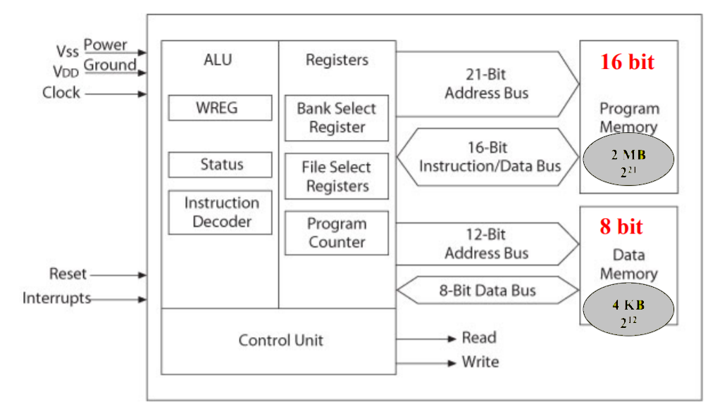
Fig. MCU and Memory
Includes Arithmetic Logic Unit (ALU), Registers, and Control Unit and Arithmetic Logic Unit (ALU)
- Performs logical and arithmetic functions
- WREG – working register (acts as an accumulator) – used to perform arithmetic or logical functions
- Status register that stores flags – indicates the status of the operation done by ALU
- Instruction decoder (ID)– when the instruction is fetched it goes into the ID to be interpreted – tell the processor what to do.
Registers – hold memory address
Bank Select Register (BSR)
4-bit register used in direct addressing the data memory.
File Select Registers (FSRs)
16-bit registers used as memory pointers in indirect addressing data memory n Program Counter (PC)
21-bit register that holds the program memory address while executing programs
Control unit- Provides timing and control signals to various Read and Write operations
Q8) Explain the data memory map of PIC 18 device?
A8)
Data Memory:
- PIC-18 has 4KB Data Memory.
- The data memory is divided into banks and each bank is 256 bytes.
- It consists of GPRs, SFRs referred as Data Registers.
- General purpose registers are used to hold dynamic data.
- SFRs are used to control the operation of Peripheral functions. Only one bank is active at a time.
- Access bank consists of lowest 96bytes and highest 160 bytes of data memory space.
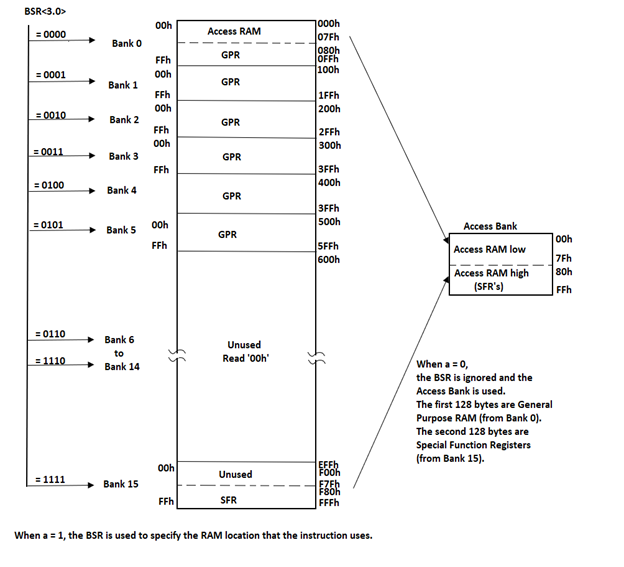
Figure. Data Memory map for PIC-18 Device.
Q9) Explain the program memory organisation of PIC-18?
A9)
Program Memory Organization:
- The program counter is 21-bit long which enables the user program to access up to 2MB program memory.
- After Power on it starts to execute the instruction from address 0
- The location 0x08 is reserved for high-priority ISR
- The location 0x18 is reserved for low-priority ISR.
- Upto 128KB of Program Memory is inside the MCU chip.
- Rest of the program memory is located outside the MCU chip.
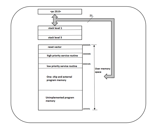
Figure. Program Memory Organization for PIC-18 device.
Q10) What are the banks of RAM explain in detail?
A10)
Four banks of Registers/RAM.
- The register/RAM in bank 0 at address between 0x000 and 0x07F
- The register/RAM in bank 1 at address between 0x080 and 0x0FF
- The register/RAM in bank 2 at address between 0x100 and 0x17F
- The register/RAM in bank 3 is at address between 0x180 and 0x1FF.
A byte at an address 0x25 accessed directly by using direct address 0x25 in the instruction. It is considered at bank 0 as 0x25 falls in bank 0 address space.
Direct Address
- A byte at an address 0x85 can be accessed by 7-bit direct address = 0x05 of Bank1
- Bank 1 base address is 0x80 and 0x85–0x80 = 0x05
Bank Pairs
- Four banks form two pairs of banks of Registers/RAM
- The register/RAM in lower bank pair is at address between 0x000 and 0x0FF
- A Bank pair needs 8-bit to access.
- The register/RAM in upper bank pair is at address between 0x100 and 0x1FF
- Bank-pair 0 address is 0x000 and 1 address is 0x100.
Register/RAM Bank Pair access
- By 8-bit address
- Bank pair is as per IRP bit
- 8-bit address is used when using indirect address for a register/RAM
- This address plus the bank-pair base address generates 9-bit address of a register/internal RAM
- Bank pair base address is as per IRP
RAM/File Register Select Register (FSR)
- FSR is used for indirect addressing in the instruction
- FSR of 8-bits
- It provides the 8-bit address of RAM/register in register file
- That address is in a bank-pair
- Bank pair is as per IRP bit in the STATUS.
IRP (indirect register-bank pair) bit
- Indirect address has 8-bits.
- These bits are taken from either lower pair of banks 0 or 1 or upper pair of banks 2 or 3
- Bit 7 in STATUS, when = 1, then upper bank-pair used
- When = 0 then lower bank pair used.
RP1-RP0 (register- pair higher bank register pair lower bank) bits
- Direct address has taken from 7-bits in the instruction
- They are taken for either bank 0 or 1 or 2 or 3.
- Bit 6-5 in STATUS, when = 11, then higher bank 3. When = 10, then bank 2. When = 01, then bank 1. When = 00, then bank 0.
Higher addresses Mirroring in all four banks
- Higher addresses 0x70-0x7F in a bank are also mirrored.
- When 0x70-0x7F is accessed, then it also means access to 0xF0H-0xFFH, 0x170-0x17F and 0x1F0-0x1FF.
- Frequently used variables are stored at these sixteen addresses by the programmer
Q11) Why we need reset operation in microcontrollers?
A11)
Reset keeps the microcontroller into known condition. For microcontroller to function properly it must be reset which means all the registers would be placed in starting position. It can be used to when trying out a device as interrupt in program execution.
For proper operation MCLR pin must be connected via resistor to positive supply. The resistor value varies between 5 and 10K. The function of the resistor is to keep certain line on logical one as preventive called as pull- up resistor.
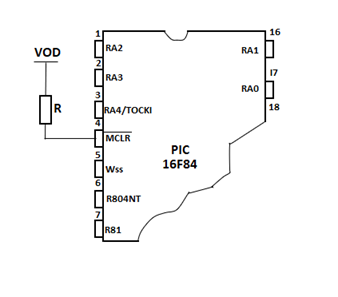
Figure. Reset
Q12) What are watch dog time. Explain its waveform and hardware too?
A12)
Watchdog timer is a hardware microcontroller. It is basically used to take out a system from an infinite loop and resets the system. Watchdog makes the embedded systems more reliable as it works as a safety mechanism.
Watchdog is a type of counter. It is an up counter which means that it counts from zero and reaches to some values. As soon the watchdog timer reaches some value its hardware generates a watchdog reset. Then the system resets this count value to zero in order to avoid system reset. The watchdog timer is loaded with some values which are based on its timeout time. The system needs to reset the counter before timeout.
Watchdog Timer Hardware
The figure below is of watchdog time hardware with input as clock. With every clock the internal counter increments. Then the comparator will compare this value with the loaded count value. Then if the comparator finds that count value matches the watchdog hardware generates and resets it.
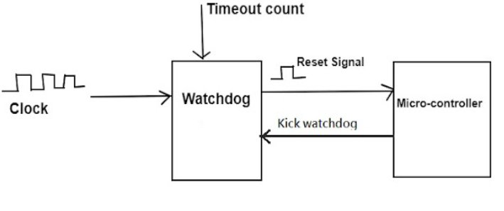
Fig. Watch dog timer
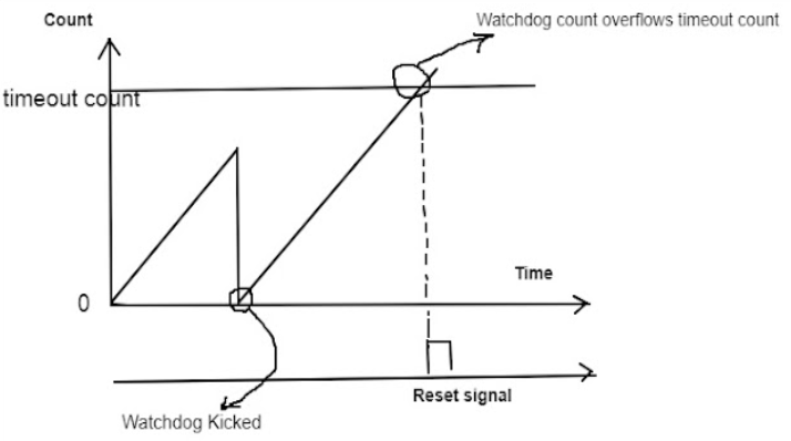
Fig. Timing Diagram
Watchdog in Microcontroller
The internal watchdog of the MSP430 family is used either as a simple timer or as a watchdog that ensures system integrity. The watchdog function is enabled after power-on reset or system reset. In case of any difficulties after start-up of MSP430, the watchdog will reset the system as often as it is needed for it to start successfully.
A system running with MCLK = 3 MHz uses the watchdog for supervision of three functions.
Power Fail — by checking the 60 Hz AC line.
Function 1 — A check is made if the software reaches this background part regularly
Function 3 — A check is made if this interrupt handler is called regularly.
Each supervised function sets a dedicated bit in RAM byte WDB in intervals less than 10.66 ms (power-up value of the watchdog with MCLK = 3 MHz) if everything is functioning normally.
The main loop checks this byte (WDB) and resets the watchdog ONLY if all three bits are set (07h). If one of the functions fails, the watchdog is not reset and will therefore reset the system.
Q13) Explain about the configuration registers of PIC microcontroller?
A13)
- Oscillators are used for timing generation. PIC microcontroller consists of external oscillators like RC oscillators or crystal oscillators.
- The crystal oscillator is connected between two oscillator pins. The value of the capacitor connected to every pin decides the mode of operation of the oscillator.
- In case of RC oscillators, the value of the resistor & capacitor determines the clock frequency and the range of clock frequency is 30KHz to 4MHz.
- In calculating software delays in pic microcontroller, the instruction execution time is determined by external clock either in oscillator or resonator.
The PIC18FXX2 operates in eight oscillator modes differently. The user can program three configuration bits (FOSC2, FOSC1, and FOSC0) and select one of these eight modes:
1. LP Low Power Crystal
2. XT Crystal/Resonator
3. HS High Speed Crystal/Resonator
4. HS + PLL High Speed Crystal/Resonator with PLL enabled
5. RC External Resistor/Capacitor
6. RCIO External Resistor/Capacitor with I/O pin enabled
7. EC External Clock
8. ECIO External Clock with I/O pin enable
Q14) How lowest current consumption can be achieved in microcontrollers?
A14)
In sleep or power down mode PIC microcontroller is placed in its lowest current consumption state. The device goes to sleep mode by executing SLEEP instruction. The device oscillator is turned off, so no system clocks are occurring in the device.
In order to minimize the power consumption in sleep mode the output ports must be sourcing or sinking the current before going to sleep mode.
Several events make the device wake up from sleep mode:
- Any device reset.
- Watch dog timer Wake-up
- Peripheral module which can set its interrupt flag while in sleep.
- Configuration bit settings
Every single bit in this register controls a specific feature, combined in this register to control all the settings (configurations), Hence they are often called the “Configuration Bits” referred as “Fuses” sometimes.
It allows the programmer to adjust to certain conditions in order to determine the operation modes of microcontroller. This state of configuration bits determines the mode in which device operates when powered.
These configuration bits are mapped to the program memory location which can be accessed at the time of programming.
Q15) Explain the addressing modes of PIC microcontroller?
A15)
The PIC microcontroller support only two addressing modes. They are
i) Direct addressing mode
Ii) Indirect addressing mode
Direct addressing mode
In this mode 7 bit of instruction identify the register file address and the 8th bit of register file address register bank select bit (RP0).
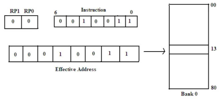
The above figure shows the method of accessing register file address 13H by direct addressing method.
Indirect addressing mode
Tn this addressing mode the 8-bit register file address is first written into a special function register (SFR) which acts as a pointer to any address location in the register file. A subsequent direct access of INDF will actually access the register file using the content of FSR pointer to the desired location of the operand.
Instruction set
- Write the instructions mnemonics in lower case
- Write special register names, RAM variable names and bit names in upper case
- Write instruction and subroutine labels in mixed case.
The instruction set of PIC is divided into three basic categories
a) Byte oriented instruction
b) Bit oriented instruction
c) Literal and control instruction
Byte oriented Instructions
In this f represents the file register and d represents destination register. The destination specifies where the result of operation is to be placed. If D=0 the result is placed in W register and if d=1, the result is placed in the file register specified in the instruction.
ADDWF f, d
CLR f
MOVWF f, d
NOP
SUBWF f, b
Bit oriented Instruction
In this b represents a bit field designator which selects the number of the bit affected by the operation and f represents the number of the file in which the bit is located.
BCF f, b
BSF f, b
BTFSC f,b
Literal and Control Instruction
In literal and control instruction K represents an 8 or 11 bit constant or literal value.
ADDLW k
ANDLW k
CALL k
MOVLW k
SUBLW k
Q16) Explain low power feature of MSP 430?
A16)
Clock System
Clock sources availability depends on the version of MSP430 microcontroller.
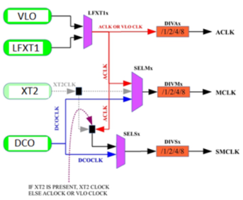
Figure. Clock System
VLOCCLK- This is a very low power/low frequency internal oscillator that can produce a frequency of 10KHz.
LFXT1CLK- (Low Frequency Crystal) – It is a crystal powered low/high frequency oscillator. It can work with either a 32Khz crystals that operate in the MHz range or external clock sources (400KHz to 16MHz range)
XT2CLK(High frequency crystal)- This is a high frequency oscillator that can be used with standard crystals resonator or external clock sources in the 400Khz to 16 MHz range.
DCOCLK- Integrated Digitally Controlled Oscillator do not use any external crystals. The DCO can generate a wide variety of frequencies ranging from few 100-kilo hertz to 10’s of MHz. It is default clock of the MSP430 after reset. The DCO clock frequency is temperature dependent.
MSP430 produces 3 different clock signals using a combination of the oscillator sources. These clock signals can be used to various peripherals like CPU, Timers, ADC etc depending upon the requirements.
MCLK- Known as main clock. It is fast high frequency clock usually used by CPU or other fast components like ADC10,ADC12, Watch Dog timer. MCLK can be sources either from LFT1CLK,DCO,VLO or XT2 oscillator. Clock signal can be divided by 1/2/4/8 using internal divider.
SMCLK- Known as Sub Main Clock. It can be sources either from LFT1CLK,DCO,VLO or XT2 oscillator. Clock signal can be divided by 1/2/4/8 using internal divider.
ACLK- known as Auxillary clock is slow,low frequency clock . It can only be sourced from LFT1CLK or VLO. Clock signal can be divided by 1/2/4/8 using internal divider. ALCK is active in all Low power modes except LPM4.
Low Power Modes
MSP430 works on two types of mode:
- Active Mode
- Low Power Modes(Standby mode)
MSP430 is designed for ultralow power applications. It offers the lowest power consumption and perfect mix of integrated peripherals for a variety of battery operated applications.
It has Low power modes LPM 0,1,2,3,4, and 3.5 and 4.5. AM is the normal running mode and all LPM for low power consideration modes. The low power operating modes consider the needs of ultralow-power consumption, speed, data throughput and minimization of individual peripheral current consumption.
LPM0- Both CPU and MCLK are disabled. SMCLK and ACLK remain active. Peripherals which use SMCLK and ACLK also remain active.
LPM1- Both CPU and MCLK are disabled. DCO is disabled. SMCLK is not available if it is sourced from DCO, ACLK remains active.
LPM2- CPU, MCLK, SMCLK and DCO are disabled, ACLK remain active.
LPM3 – CPU, MCLK, SMCLK, DCO are disabled, ACLK remain active.
LPM4- All the clocks including ACLK are disabled in this mode. The controller can only be wakened from this mode by an external interrupt. This mode consumes the least power compared to all other modes.
Clock Request Feature
The Launchpad typically uses a MSP430G2553 device that contains a Basic Clock Module+. XT1 supports both low frequency and high frequency crystals, and it integrates both DCOCLK and VLOCLK.
After power-up, MCLK and SMCLK are sourced from DCOCLK at about 1.1MHz. ACLK is sourced from LFXT1CLK in LF mode. The Launchpad comes with an option 32kHz crystal in the box that needs to be installed by the user.

Fig. Pin 18 and Pin 19 are XIN and XOUT and allow an external crystal to be connected, either 32kHz or a fast crystal.
The following code makes P2.6 and P2.7 set for accepting a crystal at the input:
MSP430 Using External 32kHz crystal
#include <msp430.h>
Void main()
{
WDTCTL = WDTPW + WDTHOLD; // Stop watchdog timer
P2SEL |= (BIT6 | BIT7); // Set P2.6 and P2.6 SEL for XIN, XOUT
P2SEL2 &= ~(BIT6|BIT7); // Set P2.6 and P2.7 SEL2 for XIN, XOUT
/* Select 32kHz Crystal for ACLK */
BCSCTL1 &= (~XTS); // ACLK = LFXT1CLK
BCSCTL3 &= ~(BIT4|BIT5); // 32768Hz crystal on LFXT1
/* Output buffered ACLK on P1.0 */
P1SEL |= BIT0;
P1SEL2 &= ~(BIT0);
P1DIR |= BIT0;
}
Low power programming and Interrupt.
To enable low power the MSP430 supports several modes, each shutting off the MSP430 more and more:
- Active Mode (AM) – Not a low power mode but rather the mode in which everything is turned on, except perhaps for some peripherals
- LPM0 – CPU and MCLK are shutoff. SMCLK and ACLK remain active.
- LPM1 – CPU and MCLK are off, as in LPM1, but DCO and DC generator are disabled if the DCO is not used for SMCLK. ACLK is active.
- LPM2 – CPU, MCLK, SMCLK and DCO are disabled, while DC generator is still enabled. ACLK is active.
- LPM3 – CPU, MCLK, SMCLK, DCO and DC generator are disabled. ACLK is active.
- LPM4 – CPU and all clocks disabled
These LPM modes refer to the individual bits in the Status Register. By setting and clearing the bits in the SR, one can turn off CPU and clocks resulting in certain Low Power Modes.
To see the power consumption
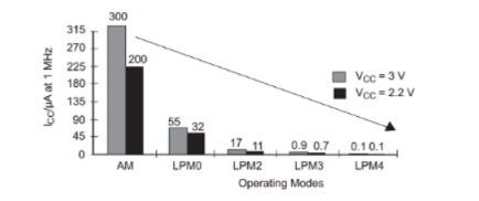
Figure. Power Consumption
At 1MHz, we go from 300uA down to less than 1uA by switching to LPM3. This is what makes the MSP430 such a good microcontroller for low power applications. It can survive for years on batteries.
Q17) What are the peripheral supports for PIC 18?
A17)
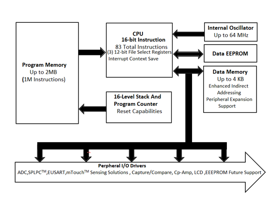
Figure. Peripherals
The PIC18 family combines maximum level of performance and integration for flexible use of 8-bit architecture.
- Internal Oscillator Up to 64 MHz.
- Flash Program Memory Up to 128 kB.
- Data EEPROM Up to 1 kB.
- SRAM Up to 8 kB.
- 32 Level Stack
- Hardware Stack Overflow and Underflow Reset Capabilities
- Vectored Interrupt Capability (VIC)
- Direct Access Memory (DAM) Controllers
- 12-bit ADC with Computation (ADC2), up to 43 channels
- Memory Access Partition (MAP)
- Device Information Area (DIA)
- Windowed Watch Dog Timer (WWDT)
- Three Complementary Waveform Generator (CWG)
- Four Configurable Logic Cell (CLC)
- Peripheral Pin Select (PPS)
- Two Comparators
- Zero Cross Detect (ZCD)
- Temperature IndicatorOn-chip
- Data Signal Modulator (DSM)
- 5-bit DAC
- Capacitive Voltage Divider (CVD)
- Up to four 10-bit PWMs
- Communication: UART, SPI, I2C, CAN, USB, Ethernet, LCD
- Extreme Low-Power (XLP)
Available in 18- to 100-pin Package