Unit-2
Combinational Logic Design
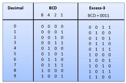
Question-1: Convert BCD to Excess 3 code.
Sol:
Question-2: Write short note on: Weighted, Non weighted and alpha numeric codes.
Sol:
Weighted Codes
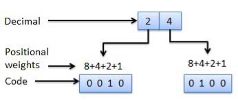
Fig.: Weighted codes
Non-Weighted Codes
Alphanumeric codes
A binary digit orbit can be represented by two symbols as '0' or '1'.
This is not sufficient for communication between two computers as we need many more symbols for communication.
These symbols represent 26 alphabetic characters with capital and small letters, numbers from 0 to 9, punctuation marks, and other symbols.
These alphanumeric codes represent numbers and alphabetic characters.
Most of them also represent other characters like symbols and various instructions necessary for conveying information.
The code at least represents 10 digits and 26 letters of alphabet i.e. total of 36 items.
Question-3: Draw and explain Full adder.
Sol:
It is developed to overcome the drawback of the Half Adder circuit.
It can add two one-bit numbers A and B and a carry C.
It is a three-input and two output combinational circuit.
Block diagram
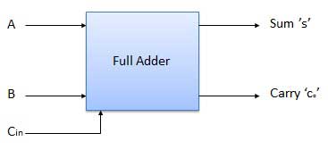
Fig.: Full adder
Truth Table
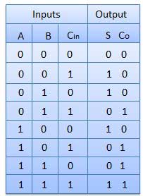
Circuit Diagram
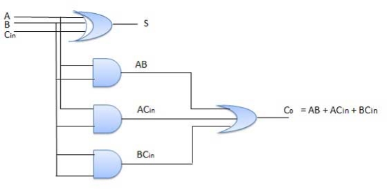
Fig.: Full adder
Question-4: Explain look ahead carry generator.
Sol:
A carry-Look ahead adder is a fast-parallel adder as it reduces the propagation delay by more complex hardware, hence it is costlier. In this design, the carry logic over fixed groups of bits of the adder is reduced to two-level logic, which is nothing but a transformation of the ripple carry design.
This method makes use of logic gates so as to look at the lower order bits of the augend and addend to see whether a higher order carry is to be generated or not.
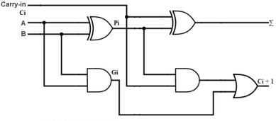
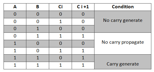
Consider the full adder circuit shown above with corresponding truth table. If we define two variables as carry generate Gi and carry propagate Pi then,
Pi = Ai ⊕ Bi
Gi = Ai Bi
The sum output and carry output can be expressed as
Si = Pi ⊕ Ci
C i +1 = Gi + Pi Ci
Where Gi is a carry generate which produces the carry when both Ai, Bi are one regardless of the input carry. Pi is a carry propagate and it is associate with the propagation of carry from Ci to Ci +1.
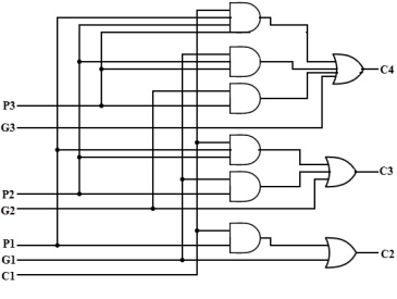
The carry output Boolean function of each stage in a 4 stage carry-Lookahead adder can be expressed as
C1 = G0 + P0 Cin
C2 = G1 + P1 C1
= G1 + P1 G0 + P1 P0 Cin
C3 = G2 + P2 C2
= G2 + P2 G1+ P2 P1 G0 + P2 P1 P0 Cin
C4 = G3 + P3 C3
= G3 + P3 G2+ P3 P2 G1 + P3 P2 P1 G0 + P3 P2 P1 P0 Cin
From the above Boolean equations we can observe that C4 does not have to wait for C3 and C2 to propagate but actually C4 is propagated at the same time as C3 and C2. Since the Boolean expression for each carry output is the sum of products so these can be implemented with one level of AND gates followed by an OR gate.
The implementation of three Boolean functions for each carry output (C2, C3 and C4) for a carry-Look ahead carry generator shown in below figure.
Question-5: Explain 2-Bit Magnitude Comparator
Sol:
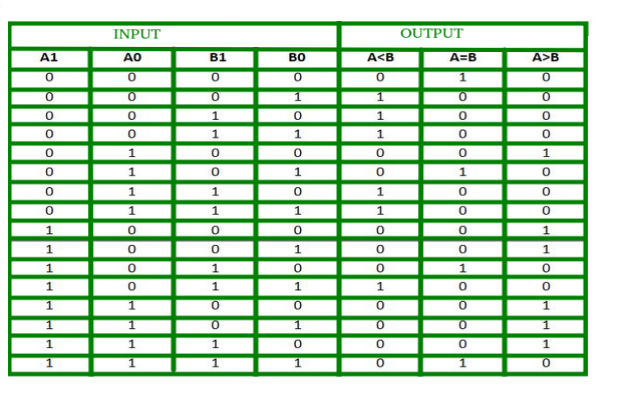
K-map for each output is as follows:
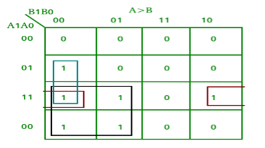
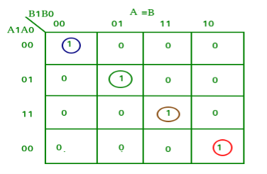
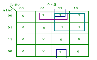
From the above K-maps output can be expressed as follows:
A>B:A1B1’ + A0B1’B0’ + A1A0B0’
A=B: A1’A0’B1’B0’ + A1’A0B1’B0 + A1A0B1B0 + A1A0’B1B0’
: A1’B1’ (A0’B0’ + A0B0) + A1B1 (A0B0 + A0’B0’)
: (A0B0 + A0’B0’) (A1B1 + A1’B1’)
: (A0 Ex-Nor B0) (A1 Ex-Nor B1)
A<B:A1’B1 + A0’B1B0 + A1’A0’B0
A logic circuit for this comparator as given below:
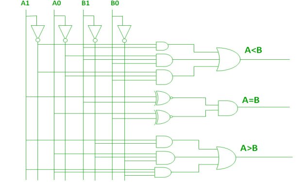
Fig:-Bit comparator
Question-6: Explain even parity generator.
Sol:
A 3-bit message is transmitted with an even parity bit. Hence assuming, the three inputs W,X and Y that are applied to the circuits and output bit is the parity bit P. The total number of 1s must be even, to generate the even parity bit P.
3- bit message | Even Parity | ||
W | X | Y | P |
0 | 0 | 0 | 0 |
0 | 0 | 1 | 1 |
0 | 1 | 0 | 1 |
0 | 1 | 1 | 0 |
1 | 0 | 0 | 1 |
1 | 0 | 1 | 0 |
1 | 1 | 0 | 0 |
1 | 1 | 1 | 1 |
The K-map simplification for 3-bit message even parity generator is
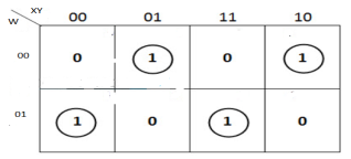
From the above K-Map, the expression is:
P=W′X′Y+W′XY′+WX′Y′+WXY
P=W′(X′Y+XY′)+W(X′Y′+XY)
P=W′(X⊕Y)+W(X⊕Y)′=W⊕X⊕Y

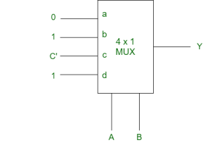
Question-7: For a given SOP function f(A, B, C) = m(0, 1, 4, 6, 7) draw MUX for 3 variable function.
Sol:
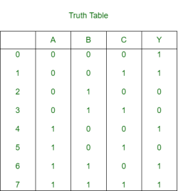
Let A and B are the select lines and C be the input,
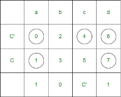
Thus, for the implementation of given logical function, required is one 4×1 MUX and and inverter.
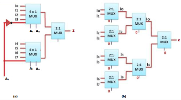
Question-8: Design 8:1 Mux using two 4:1 Multiplexers.
Sol:
