Unit 4
Algorithmic State Machines and Programmable Logic Devices
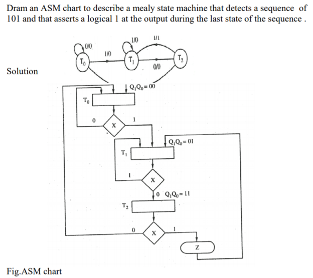
Question-1: Explain Basic Components of ASM charts.
Sol: Following are the three basic components of ASM charts.
State box
State box is represented in rectangular shape. Each state box represents one state of the sequential circuit. The symbol of state box is shown in the following figure.
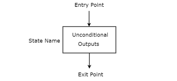
It is having one entry point and one exit point. Name of the state is placed to the left of state box. The unconditional outputs corresponding to that state can be placed inside state box. Moore state machine outputs can also be placed inside state box.
Decision box
Decision box is represented in diamond shape. The symbol of decision box is shown in the following figure.
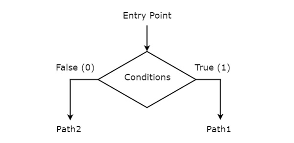
It is having one entry point and two exit paths. The inputs or Boolean expressions can be placed inside the decision box, which are to be checked whether they are true or false. If the condition is true, then it will prefer path1. Otherwise, it will prefer path2.
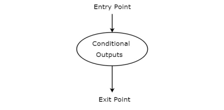
Conditional output box
Conditional output box is represented in oval shape. The symbol of conditional output box is shown in the following figure.
Question-2:
Question-3: Define FSM and ASM.
Sol: Finite State Machines (FSM)
A synchronous sequential circuit is also called as Finite State Machine FSM, if it has finite number of states. There are two types of FSMs.
ASM
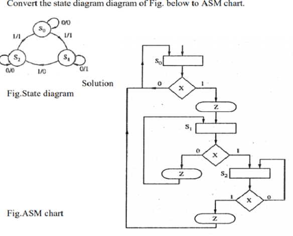
Every digital system can be partitioned into two parts. Those are data path digital circuits and control circuits. Data path circuits perform the functions such as storing of binary information data and transfer of data from one system to the other system. Whereas, control circuits determine the flow of operations of digital circuits.
It is difficult to describe the behavior of large state machines using state diagrams. To overcome this difficulty, Algorithmic State Machine ASM charts can be used. ASM charts are similar to flow charts. They are used to represent the flow of tasks to be performed by data path circuits and control circuits.
Question-4:
Question-5: Draw and explain PROM in detail.
Sol: A programmable read-only (PROM) memory is a device which permanently stores binary information. It differs from a normal ROM because it can be programmed electrically once using a PROM programmer. This programmable logic device has Fixed AND arrays and Programmable OR arrays. The block diagram of a PROM is shown below:

It consists of n input lines and m output lines. Each bit combination of the input variables is called an address. Each bit combination that comes out of the output line is called a word. The number of bits per word is equal to the number of output lines, m. The address specified in binary number denotes one of the minterms of n variables. The number of distinct addresses possible with n-input variables is 2n. An output word can be selected by a unique address, and since there are 2n distinct addresses in a PROM, there are 2n distinct words in the PROM. The word available on the output lines at any given time depends on the address value applied to the input lines.
Consider a 64x4 PROM. The PROM consists of 64 words of 4 bits each. This means that there are 4 output lines and particular word from 64 words presently available on the output lines is determined from the six input lines. There are only 6 inputs in a 64X4 PROM because 26 =64, and with six variables we can specify 64 addresses or min terms. For each address input, there is a unique selected word. Thus if the input address is 00000, word number 0 is selected and applied to the output lines. The following figure shows the internal logic construction of a 64X4 PROM.
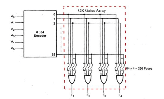
The six input variables are decoded in 64 lines by means of 64 AND Gates and 6 inverters. Each output of the decoder represents one of the minterms of the six variables. The 64 outputs of the decoder are connected through fuses to each OR Gate. Only 4 fuses are shown in the diagram, but actually each OR gate has 64 inputs and each input goes through a fuse that can be blown as desired.
Thus each output provides the sum of all the minterms on n-input variables. We also know that any Boolean function can be expressed in sum of minterms form. By breaking the links of those minterms not included in the function, each PROM output can be made to represent the Boolean function of one of the output variables in the combinational circuit. For an n-input, m-output combinational circuit, we need a 2n x m PROM.
Question-6: Explain PLA.
Sol: The combinational circuit do not use all the min terms every time. Occasionally they have don’t care conditions. Don’t care condition when implemented with a PROM becomes an address input that will never occur. The result is that not all the bit patterns available in the PROM are used, which may be considered a waste of available equipment.
For cases where the number of don’t care conditions is excessive, it is more economical to use Programmable Logic Array (PLA). The concept is similar to PROM, however it does not generate all the min terms as in the case of PROM. It has both sections of the AND and OR Arrays as programmable, i.e. there is a Programmable AND Array and Programmable OR Array as well. (both AND and OR gates have fuses at the inputs).
The following figure shows the block diagram of PLA:

It consists of n-inputs, m outputs, k-product terms and m sum terms. The product terms constitute a group of k AND gates and the sum terms constitute a group of m OR gates. Fuses are inserted between all n inputs and their complement values to each of the AND gates. Fuses are also provide between the outputs of the AND gates and the inputs of the OR Gates. The third set of fuses in the output inverters allows the output function to be generated either in the AND-OR form or in the AOI form.
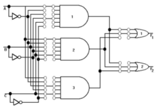
The following figure shows the internal construction of PLA having 3-inputs, 3 product terms and two outputs. The size of the PLA is specified by the number of inputs, the number of product terms and the number of outputs.
Question-7: Explain PAL.
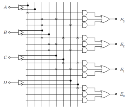
Sol: Programmable array logic (PAL) is a programmable logic device with a fixed OR array and a programmable AND array. Because only AND gates are programmable, PAL is easier to program, but is not as flexible as the PLA. Figure below shows the array logic of typical PAL.
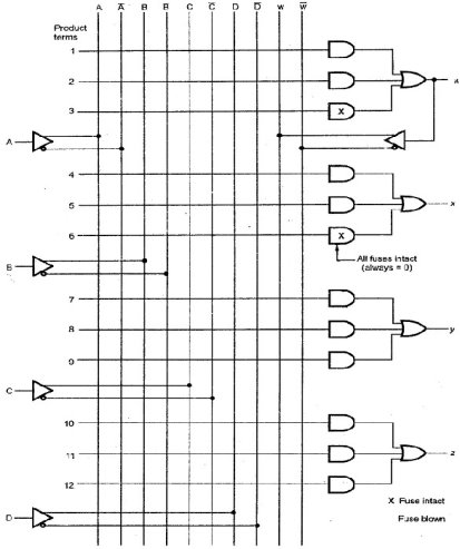
It has 4 inputs and 4 outputs. Each input has buffer and inverter gate. Please note that two gates are shown with one composite graphic symbol with normal and complement outputs. Each section in the figure has three programmable AND gates and one fixed OR gate. The output of section 1 is connected to a buffer-inverter gate and then feedback into the inputs of the AND gates, through fuses. This allows the logic designer to feed an output function back as an input variable to create a new function.
Question-8: Design a BCD-to-Excess3 code converter using
(a) PROM (b) PLA (c) PAL
Sol: The BCD to Excess-3 code converters truth table is given below:
(a) For the design using PROM, a PROM size of 10x4 is required, but since PROM of this size does not exist, therefore a PROM size of 16x4 is to be used. Data is to be stored in the PROM at the addresses corresponding to the BCD code, the data is the Excess-3 code. For example, at the address 000, the data stored is 0011 and at the address 1001 the data stored is 1100.
(b) Logical expressions can be written for E3, E2, E1, E0 outputs in terms of A, B, C, D inputs. To reduce the hardware requirements, these expressions can be minimized using K-Maps.
The simplified expressions are:
E3= A+BC+BD
E2= BC’D’+B’C+B’D
E1=C’D’+CD
E0=D’
The size of the PLA required is:
No. Of inputs = 4
No. Of Outputs = 4
No. Of product terms = 9
Thus the circuit can be realized as follows:
(c) The required size of PAL is
No. Of inputs = 4
No. Of outputs = 4
Minimum number of AND Gates for each output = 3
Thus the circuit can be realized as follows:
