Unit 2
Design of sequential circuit
Q1)What is a sequential circuit ?
A1)
A Sequential circuit consists of inputs variable (X), logic gates, and output variable (Z).
A combinational circuit generates an output based on the input variable only but the Sequential circuit produces an output based on the current input and previous output variables.
This means that it includes memory elements which are capable of storing binary information.
Q2)What are the types of sequential circuit ?
A2)
There are two types of the sequential circuit :
Asynchronous sequential circuit –
- They do not use a clock signal but instead uses the pulses as inputs.
- These circuits are faster because there is a clock pulse and can change their state immediately when there is a change in the input signal.
- It is used when the speed of operation is important and is independent of the internal clock pulse.

Fig. 3 Asynchronous Sequential circuit
But they are more difficult to design and their output is also uncertain.
Synchronous sequential circuit –
- This circuit uses clock signal and level inputs.
- The output pulse is received in the same duration as the clock pulse for the clocked sequential circuits.
- They wait for the next clock pulse to arrive to perform the next operation, these circuits are a bit slower as compared to asynchronous circuits.
- Level output changes state at the start of an input pulse and remains in that state until the next input or clock pulse arrives.
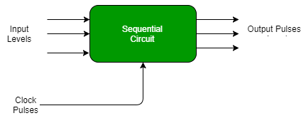
Fig. 4 Synchronous Sequential circuit
- It is used in synchronous counters, flip flops, and in MOORE-MEALY machines.
- It is also used to design Counters, Registers, RAM, etc
Q3) Design of synchronous circuits?
A3)
Asynchronous Counter
This universal clock is not used and only the first flip flop is driven by the main clock and the clock input of the rest of the following is driven by the output of previous flip flops. 
Fig. 10 Asynchronous counter
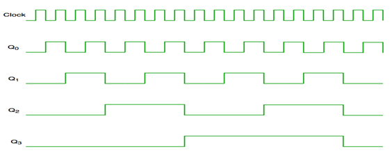
Fig. 5 Timing diagram of Asynchronous counter
It is seen from the timing diagram that Q0 is changing as soon as the rising edge of the clock pulse is encountered.
Q1 is changing when the rising edge of Q0 is encountered and so on.
In this way, ripples are generated through Q0, Q1, Q2, Q3 and therefore it is also called a RIPPLE counter.
Q4) Design synchronous counters?
A4)
It has one global clock which drives each and every flip flop and hence output changes in parallel.
The advantage of synchronous counter over the asynchronous counter is that it can operate on a higher frequency and it does not have a cumulative delay.
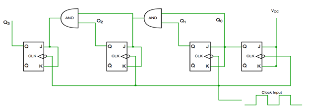
Synchronous counter
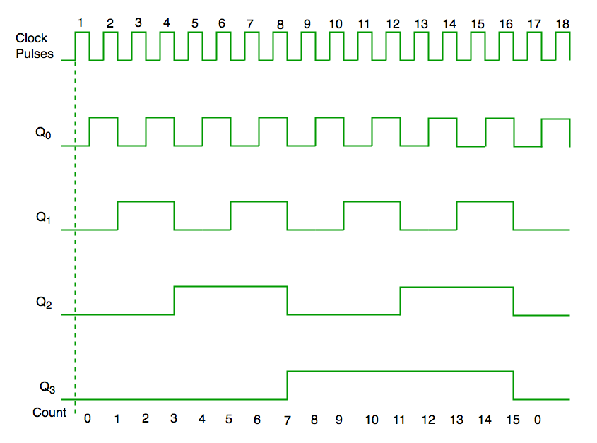
Fig. The timing diagram of synchronous counter
Q5) Explain up-down counters?
A5)
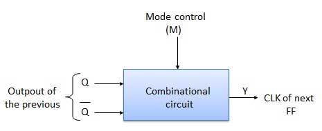
Up counter and down counter is combined together to obtain an UP/DOWN counter. A mode control (M) input is also provided to select either up or down mode. A combinational circuit is required to be designed and used between each pair of flip-flop in order to achieve the up/down operation.
- Type of up/down counters
- UP/DOWN ripple counters
- UP/DOWN synchronous counter
UP/DOWN Ripple Counters
In the UP/DOWN ripple counter all the FFs operate in the toggle mode. So either T flip-flops or JK flip-flops are to be used. The LSB flip-flop receives clock directly. But the clock to every other FF is obtained from (Q = Q bar) output of the previous FF.
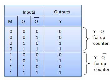
- UP counting mode (M=0) − The Q output of the preceding FF is connected to the clock of the next stage if up counting is to be achieved. For this mode, the mode select input M is at logic 0 (M=0).
- DOWN counting mode (M=1) − If M = 1, then the Q bar output of the preceding FF is connected to the next FF. This will operate the counter in the counting mode.
Example
3-bit binary up/down ripple counter.
- 3-bit − hence three FFs are required.
- UP/DOWN − So a mode control input is essential.
- For a ripple up counter, the Q output of preceding FF is connected to the clock input of the next one.
- For a ripple up counter, the Q output of preceding FF is connected to the clock input of the next one.
- For a ripple down counter, the Q bar output of preceding FF is connected to the clock input of the next one.
- Let the selection of Q and Q bar output of the preceding FF be controlled by the mode control input M such that, If M = 0, UP counting. So connect Q to CLK. If M = 1, DOWN counting. So connect Q bar to CLK.
Block Diagram
Truth Table
Q6) Explain shift registers?
A6)
Shift registers
- Flip flops are used to store one bit of binary data (1or 0).
- If we need to store multiple bits of data, we use multiple flip flops.
- N flip flops are connected to store n bits of data.
- A Register is a device that stores such information. It is a group of flip flops connected in series which is used to store multiple bits of data.
- The information stored in these registers can be transferred with the help of shift registers.
- This register is a group of flip flops used to store multiple bits of data.
- The bits stored in these registers can be moved in/out of the registers by applying clock pulses.
- The registers which shift the bits towards left are called “Shift left registers”.
The registers which shift the bits towards the right are called “Shift right registers”.
Q7) Explain the types of shift registers ?
A7)
Shift registers are of 4 types and they are:
- Serial In Serial Out register
- Serial In the parallel Out register
- Parallel In Serial Out register
- Parallel In the parallel Out register
Serial-In Serial-Out Shift Register (SISO) –
- It allows serial input i.e. one bit after another and produces a serial output is known as Serial-In Serial-Out shift register.
- Since it has one output, the data leaves the register one bit at a time in a serial pattern, hence known as Serial-In Serial-Out Shift Register.
- The logic circuit is given underneath.
- The circuit comprises four D flip-flops which are connected serially.
- All these flip-flops are synchronous in nature

Fig. SISO
Serial-In Parallel-Out shift Register (SIPO) –
- It allows serial input through a single data line and produces a parallel output.
- The logic circuit is given underneath.
- The circuit consists of four D flip-flops which are connected synchronously.
- The clear (CLR) signal is also connected to all the 4 flip flops in order to RESET them.
- The output of the first flip flop is sent to the input of the next and so on.
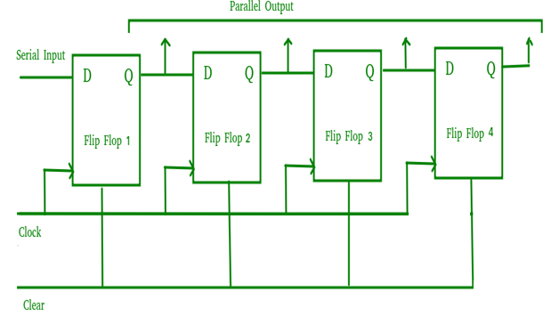
Fig. SIPO
- They are used in communication lines because the main use of the SIPO register is to convert serial data into parallel data.
Parallel-In Serial-Out Shift Register (PISO) –
- It allows parallel input data and produces a serial output.
- The logic circuit is given underneath.
- The circuit comprises four D flip-flops which are connected synchronously.
- The clock is connected to all the flip flops but the input data is connected to each flip flop individually through a multiplexer.
- The output of the previous flip flop and parallel data input are connected to the input of the MUX and the output of MUX is connected to the next flip flop.
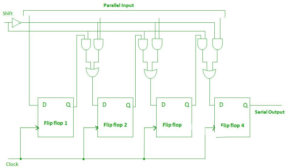
Fig. PISO
- It used to convert parallel data to serial data.
Parallel-In Parallel-Out Shift Register (PIPO) –
- It allows parallel input data and produces a parallel output.
- The logic circuit is given underneath.
- The circuit comprises four D flip-flops which are connected synchronously.
- The clear (CLR) and clock signals are connected to all flip flops.
- In this, there are no interconnections between flip-flops as no serial shifting of the data is required.
- Data is provided separately as input for each flip flop and the output is also collected individually from each flip flop.
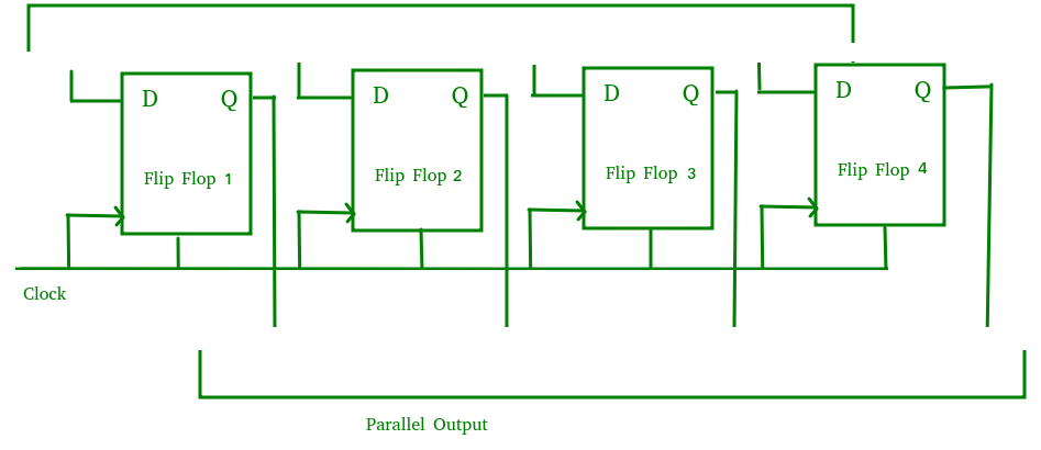
Fig. PIPO
- It is used as a temporary storage device and it acts as a delay element too.
Q8) Explain ring counters?
A8)
Ring counter is a typical application of Shift resister. Ring counter is almost same as the shift counter. The only change is that the output of the last flip-flop is connected to the input of the first flip-flop in case of ring counter but in case of shift resister it is taken as output. Except this all the other things are same.
No. Of states in Ring counter = No. Of flip-flop used
So, for designing 4-bit Ring counter we need 4 flip-flop.
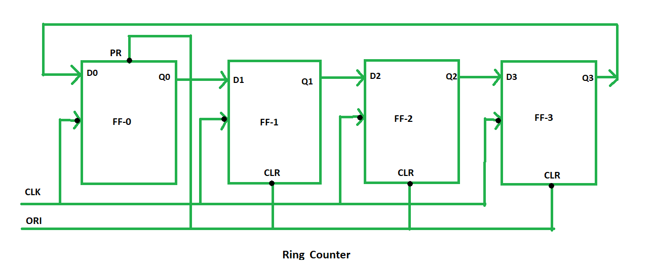
In this diagram, we can see that the clock pulse (CLK) is applied to all the flip-flop simultaneously. Therefore, it is a Synchronous Counter.
Also, here we use Overriding input (ORI) to each flip-flop. Preset (PR) and Clear (CLR) are used as ORI.
When PR is 0, then the output is 1. And when CLR is 0, then the output is 0. Both PR and CLR are active low signal that is always works in value 0.
PR = 0, Q = 1
CLR = 0, Q = 0
These two values are always fixed. They are independent with the value of input D and the Clock pulse (CLK).
Working –
Here, ORI is connected to Preset (PR) in FF-0 and it is connected to Clear (CLR) in FF-1, FF-2, and FF-3. Thus, output Q = 1 is generated at FF-0 and rest of the flip-flop generate output Q = 0. This output Q = 1 at FF-0 is known as Pre-set 1 which is used to form the ring in the Ring Counter.
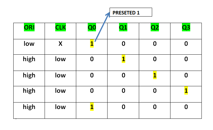
This Preseted 1 is generated by making ORI low and that time Clock (CLK) becomes don’t care. After that ORI made to high and apply low clock pulse signal as the Clock (CLK) is negative edge triggered. After that, at each clock pulse the preseted 1 is shifted to the next flip-flop and thus form Ring.
From the above table, we can say that there are 4 states in 4-bit Ring Counter.
4 states are:
1 0 0 0
0 1 0 0
0 0 1 0
0 0 0 1
In this way can design 4-bit Ring Counter using four D flip-flops.
Q9) Explain twisted ring counter?
A9)
Twisted Ring Counter –
It is also known as switch-tail ring counter, walking ring counter or Johnson counter. It connects the complement of the output of the last shift register to the input of the first register and circulates a stream of ones followed by zeros around the ring.
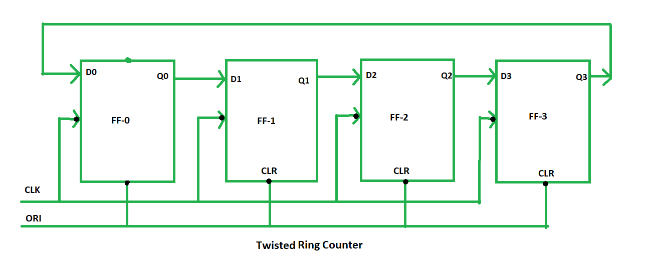
Here, we use Clock (CLK) for all the flip-flops.
Q10) What are the applications of counters?
A10)
- Frequency counters
- Digital clock
- Time measurement
- A to D converter
- Frequency divider circuits
- Digital triangular wave generator.