Unit 3
Digital memories and logic families
Q1) Explain SRAM ?
A1)
Static RAM (SRAM)
Here, the memory possesses its contents as long as power is being supplied. As the power gets down, data is lost due to volatile nature.
It uses a matrix of 6-transistors and no capacitors. Transistors do not require power to prevent leakage, so servicing is not required regularly.
There is an extra space in the matrix, so more chips are used than DRAM for the same amount of storage, thus raising the manufacturing cost.
It is used as a cache memory with fast access.
Characteristic of Static RAM
- Long life
- No change required
- Fast
- Used as cache memory
- Large in size
- Expensive
- High power consumption
Q2) Explain Dynamic RAM ?
A2)
Dynamic RAM (DRAM)
DRAM needs to be continuously refreshed in order to maintain the data.
This can be done by placing the memory on a refresh circuit that rewrites the data several hundred times per second.
It is used for system memory and is cheap and small.
All DRAMs are made up of memory cells, comprising of one capacitor and one transistor.
Characteristics of Dynamic RAM
- Short data lifetime
- Needs to be refreshed continuously
- Slow as compared to SRAM
- Small in size
- Low cost
Low power consumption
Q3) Explain ROM ?
A3)
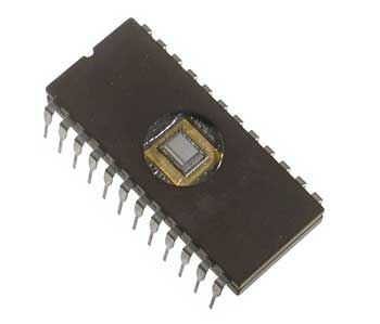
ROM stands for Read-Only Memory.
It can only read but cannot write on it.
This memory is non-volatile.
The information is stored permanently during manufacturing.
It stores instructions that are required to start a computer and are referred to as bootstrap.
They are not only used in the computer but also in other electronic devices like washing machine, microwave oven, etc.
Advantages :
- Non-volatile in nature
- Cheaper than RAMs
- Easy to test
- More reliable
Q4) What are the types of ROM ?
A4)
- Programmable Read-Only Memory (PROM)
- Electrically Programmable Read-Only Memory (EPROM)
- Electrically Erasable Programmable Read-Only Memory (EEPROM; also called Flash ROM)
- Electrically Alterable Read-Only Memory (EAROM)
Q5) Explain PAL ?
A5)
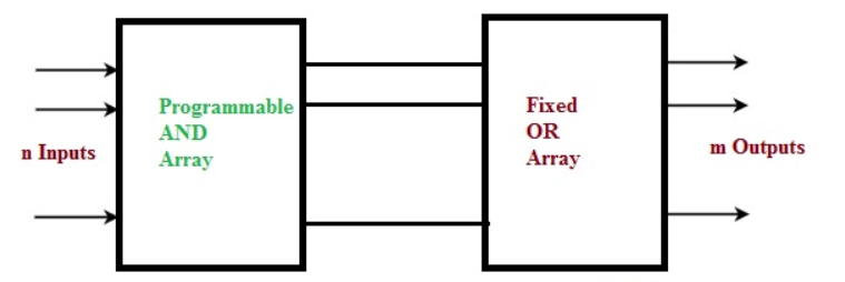
Both Programmable Array Logic and Programmable Logic Array are types of PLDs (programmable logic devices), and these are mainly used for designing combination logic mutually by sequential logic.
Programmable Array Logic
The designing of the programmable array logic can be done with fixed OR gates as well as programmable AND gates.
By using this we can implement two easy functions wherever the associates AND gates with each OR gate denote the highest number of product conditions that can be produced in the form of SOP (sum of product) of an exact function.
As the logic gates like AND is connected continually toward the OR gates, and that indicates that the produced product term is not distributed with the output functions. The major notion behind PLD development is to fabricate a compound Boolean logic onto a single chip by removing the defective wiring, avoiding the logic design, as well as decreasing the consumption of power.
Example of PAL
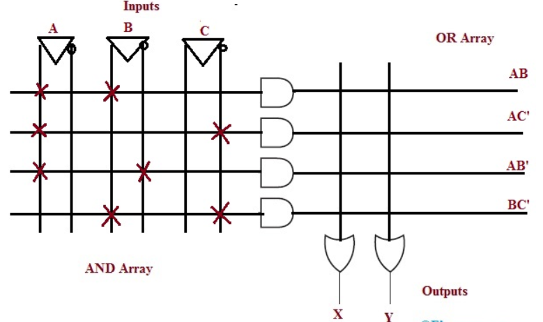
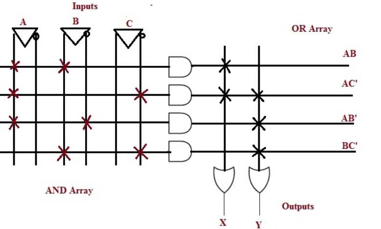
Implement the following Boolean expression with the help of programmable array logic (PAL)
X=AB + AC’
Y= AB’ + BC’
The above given two Boolean functions are in the form of SOP (sum of products). The product terms present in the Boolean expressions are X & Y, and one product term that is AC’ is common in every equation.
So, the total required logic gates for generating the above two equations is AND gates-4 OR programmable gates-2.
The equivalent PAL logic diagram is shown below.
PAL Logic Circuit
The AND gates which are programmable have the right of entry for normal as well as complemented variable inputs. In the above logic diagram, the available inputs for each AND gate are A, A’, B, B’, C, C’. So, in order to generate a single product term with every AND gate, the program is required.
All the product terms are obtainable at the inputs of an each OR gate. Here, the programmable connections on the logic gate can be denoted with the symbol ‘X’.
Here, the OR gate inputs are fixed. Thus, the required product terms are associated with each OR gate inputs. As a result, these gates will generate particular Boolean equations. The ‘.’ The symbol represents permanent connections.
Q6) Explain PLA ?
A6)
Design of Programmable Logic Array (PLA)
The definition of term PLA presents the Boolean function in the form of a sum of product (SOP). The designing of this programmable logic array can be done using the logic gates like AND, OR, and NOT by fabricating on the chip, that makes every input as well as its compliment obtainable toward every AND gate.
An every AND gate’s output is connected to the every OR gate. Finally, the output of the OR gate generates the output of the chip. Thus, this is how an appropriate association is finished to use the expressions of the sum of the product. In the programmable logic array, the connections of logic gates like AND & OR are programmable.
Example of PLA
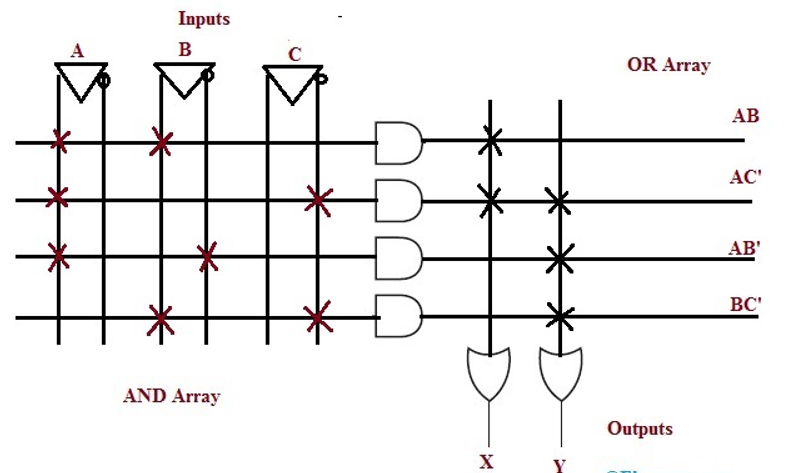
Implement the following Boolean expression with the help of programmable logic array (PLA)
X = AB + AC’
Y = AB’ +BC + AC’
The above given two Boolean functions are in the form of SOP (sum of products). The product terms present in the Boolean expressions are X & Y, and one product term that is AC’ is common in every equation. So, the total required logic gates for generating the above two equations is AND gates-4, OR programmable OR gates-2. The equivalent PLA logic diagram is shown below.
PLA Logic Circuit
The AND gates which are programmable have the right of entry for normal as well as complemented variable inputs. In the above logic diagram, the available inputs for each AND gate are A, A’, B, B’, C, C’. So, in order to generate a single product term with every AND gate, the program is required.
All the product terms are obtainable at the inputs of each OR gate. Here, the programmable connections on the logic gate can be denoted with the symbol ‘X’.
Q7) Explain CPLD?
A7)
Complex Programmable Logic Device
A complex programmable logic device (CPLD), is a complex device than programmable logic devices discussed in previous sections. CPLD contains the circuitry similar to PAL devices. Figure below shows the typical CPLD architecture having four function blocks of PLDs.
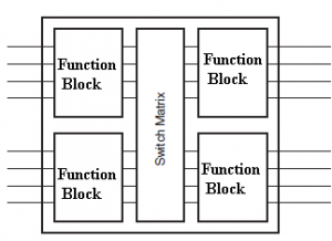
The function blocks has programmable interconnections. A switch matrix is used for function blocks to function blocks interconnections. Further, switch matrix in a CPLD may or may not be fully connected. This shows that, some of the connections between function block outputs and inputs are not supported in the CPLD. The complexity of a typical PAL device is around few hundred logic gates whereas the complexity of CPLD is around tens of thousands of logic gates. The CPLDs has predictable timing characteristics hence are suitable for critical control applications and other applications where a high performance level is required. Further, due to low power consumption and low cost, CPLDs are mostly used for battery-operated portable applications such as mobile phones, digital assistants etc.
Q8) Explain FPGA ?
A8)
The field programmable gate array is an integrated circuit that consists of internal hardware blocks with user-programmable interconnects to customize operation for a specific application.
The interconnects can readily be reprogrammed, allowing an FPGA to accommodate changes to a design or even support a new application during the lifetime of the part.
The FPGA has its roots in earlier devices such as programmable read-only memories (PROMs) and programmable logic devices (PLDs). These devices could be programmed either at the factory or in the field, but they used fuse technology (hence, the expression “burning a PROM”) and could not be changed once programmed.
In contrast, FPGA stores its configuration information in a re-programmable medium such as static RAM (SRAM) or flash memory.
Q9) Explain the architecture of FPGA?
A9) A basic FPGA architecture consists of thousands of fundamental elements called configurable logic blocks (CLBs) surrounded by a system of programmable interconnects, called a fabric, that routes signals between CLBs. Input/output (I/O) blocks interface between the FPGA and external devices.
Depending on the manufacturer, the CLB may also be referred to as a logic block (LB), a logic element (LE) or a logic cell (LC).
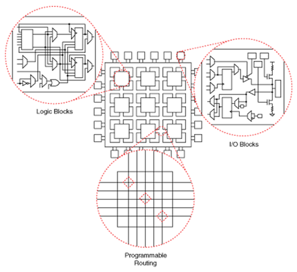
An individual CLB as shown in figure is made up of several logic blocks. A lookup table (LUT) is a characteristic feature of an FPGA. An LUT stores a predefined list of logic outputs for any combination of inputs: LUTs with four to six input bits are widely used. Standard logic functions such as multiplexers (mux), full adders (FAs) and flip-flops are also common.
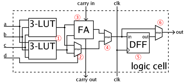
The number and arrangement of components in the CLB varies by device; the simplified example in Figure 2 contains two three-input LUTs (1), an FA (3) and a D-type flip-flop (5), plus a standard mux (2) and two muxes, (4) and (6), that are configured during FPGA programming.
This simplified CLB has two modes of operation. In normal mode, the LUTs are combined with Mux 2 to form a four-input LUT; in arithmetic mode, the LUT outputs are fed as inputs to the FA together with a carry input from another CLB. Mux 4 selects between the FA output or the LUT output. Mux 6 determines whether the operation is asynchronous or synchronized to the FPGA clock via the D flip-flop.
Current-generation FPGAs include more complex CLBs capable of multiple operations with a single block; CLBs can combine for more complex operations such as multipliers, registers, counters and even digital signal processing (DSP) functions.
Q10) Mention the applications of FPGA ?
A10)
Many applications rely on the parallel execution of identical operations; the ability to configure the FPGA’s CLBs into hundreds or thousands of identical processing blocks has applications in image processing, artificial intelligence (AI), data center hardware accelerators, enterprise networking and automotive advanced driver assistance systems (ADAS).
Many of these application areas are changing very quickly as requirements evolve and new protocols and standards are adopted. FPGAs enable manufacturers to implement systems that can be updated when necessary.
A good example of FPGA use is high-speed search: Microsoft is using FPGAs in its data centers to run Bing search algorithms. The FPGA can change to support new algorithms as they are created. If needs change, the design can be repurposed to run simulation or modeling routines in an HPC application. This flexibility is difficult or impossible to achieve with an ASIC.
Other FPGA uses include aerospace and defense, medical electronics, digital television, consumer electronics, industrial motor control, scientific instruments, cybersecurity systems and wireless communications.