Unit 5
Other Analog circuits
Q1) What is an active filter?
A1)
If an active filter permits only low-frequency components and denies all other high-frequency components, then it is termed as an Active Low Pass Filter.
Active low pass filters are made up of Op-Amp.
The input to the Op-Amp is high impedance signals, which produces a low impedance signal as output.
The performance of the amplifier plays a very important factor when designing an active low pass filter.
There are two primary kinds of active low-pass filters namely switched capacitor type and continuous capacitor type. The filters are available from first-order until eight order of design.
It is a simplistic filter that is composed of only one reactive component Capacitor accompanying with an active component Op-Amp.
A resistor is utilized with the capacitor or inductor to form RC or RL low pass filter respectively. In a passive circuit, the output signal amplitude is smaller than the input signal amplitude.
When a passive low pass filter is connected to an Op-Amp either in inverting or non-inverting condition, it gives an active low pass filter design. The connection of a simple RC circuit with a single Op-Amp is shown in the image below.
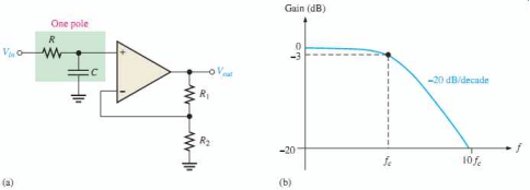
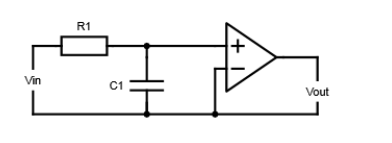
When compared with passive filter, an active filter has an arrangement in which the amplifier is designed as a voltage follower (Buffer) which gives a DC gain of one. This configuration provides excellent stability to the filter and has a high power gain. The main drawback of this filter is that it has no voltage gain above one, which can be rectified with extra circuit design.
Q2) Explain first order low pass filter?
A2)
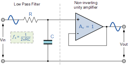
This first-order low pass active filter, consists simply of a passive RC filter stage providing a low frequency path to the input of a non-inverting operational amplifier. The amplifier is configured as a voltage-follower (Buffer) giving it a DC gain of one, Av = +1 or unity gain as opposed to the previous passive RC filter which has a DC gain of less than unity.
The advantage of this configuration is that the op-amps high input impedance prevents excessive loading on the filters output while its low output impedance prevents the filters cut-off frequency point from being affected by changes in the impedance of the load.
While this configuration provides good stability to the filter, its main disadvantage is that it has no voltage gain above one. However, although the voltage gain is unity the power gain is very high as its output impedance is much lower than its input impedance. If a voltage gain greater than one is required we can use the following filter circuit.
Active Low Pass Filter with Amplification
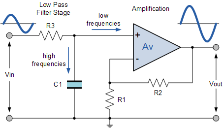
The frequency response of the circuit will be the same as that for the passive RC filter, except that the amplitude of the output is increased by the pass band gain, AF of the amplifier.
For a non-inverting amplifier circuit, the magnitude of the voltage gain for the filter is given as a function of the feedback resistor ( R2 ) divided by its corresponding input resistor ( R1 ) value and is given as:
DC gain = (1+ R2/R1)
Therefore, the gain of an active low pass filter as a function of frequency will be:
Gain of a first-order low pass filter
Voltage gain (Av) = Vout /Vin = AF /  1 + (f/fc) 2
- Where:
- AF = the pass band gain of the filter, (1 + R2/R1)
- ƒ = the frequency of the input signal in Hertz, (Hz)
- ƒc = the cut-off frequency in Hertz, (Hz)
Thus, the operation of a low pass active filter can be verified from the frequency gain equation above as:
- 1. At very low frequencies, ƒ < ƒc Vout / Vin ͌ AF
- 2. At the cut-off frequency, ƒ = ƒc Vout / Vin = AF /

- 3. At very high frequencies, ƒ > ƒc Vout / Vin < AF
Thus, the Active Low Pass Filter has a constant gain AF from 0Hz to the high frequency cut-off point, ƒC.
At ƒC the gain is 0.707AF, and after ƒC it decreases at a constant rate as the frequency increases. That is, when the frequency is increased tenfold (one decade), the voltage gain is divided by 10.
In other words, the gain decreases 20dB (= 20*log(10)) each time the frequency is increased by 10. When dealing with filter circuits the magnitude of the pass band gain of the circuit is generally expressed in decibels or dB as a function of the voltage gain, and this is defined as:
Magnitude of Voltage Gain in (dB)
AV(dB) = 20 log 10 (Vout/Vin )
-3 dB = 20 log 10 (0.707 Vout/Vin)
Q3) Design a non-inverting active low pass filter circuit that has a gain of ten at low frequencies, a high frequency cut-off or corner frequency of 159Hz and an input impedance of 10KΩ.
A3) The voltage gain of a non-inverting operational amplifier is given as:
Af = 1 + R2 / R1 =10
Assume a value for resistor R1 of 1kΩ rearranging the formula above gives a value for R2 of:
R2 = (10 -1) x R1 = 9 x 1 k = 9 k Ω
So for a voltage gain of 10, R1 = 1kΩ and R2 = 9kΩ. However, a 9kΩ resistor does not exist so the next preferred value of 9k1Ω is used instead. Converting this voltage gain to an equivalent decibel dB value gives:
Gain in dB = 20 log A = 20 log 10 = 20dB.
The cut-off or corner frequency (ƒc) is given as being 159Hz with an input impedance of 10kΩ. This cut-off frequency can be found by using the formula:
Fc = 1/ 2 π RC Hz where fc = 159Hz and R = 10kΩ
By rearranging the above standard formula we can find the value of the filter capacitor C as:
C = 1/ 2 π fc R = 1/ 2π x 159 x 10 K = 100nF
Q4) Explain monostable multi-vibrator?
A4)
The monostable multivibrator is also called as the one-shot multivibrator. The circuit produces a single pulse of specified duration in response to each external trigger signal. For such a circuit, only one stable state exists.
When an external trigger is applied, the output changes its state. The new state is called as a quasi-stable state. The circuit remains in this state for a fixed interval of time.
After some time it returns back to its original stable state. In fact, an internal trigger signal is generated which drives the circuit back to its original stable state. Usually, the charging and discharging of a capacitor provide this internal trigger signal.
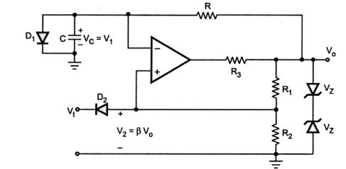
- The diode D1 connected across the capacitor is called clamping diode. It clamps the capacitor voltage to 0.7V when the output is at + Vsat .
- A negative triggering pulse is applied to the Non-inverting terminal of Op-amp through RC differentiator circuit and diode D2.
Operation of the Circuit
(i). To understand the operation of the circuit, let us assume that the output Vo is at +Vsat that is in its stable state.
(ii). The diode D1 (Connected across Capacitor) conducts and the voltage across the capacitor C - Vc gets clamped to 0.7 Volts.
(iii). The voltage at the non-inverting terminal is controlled by voltage divider circuit of R1 and R2
Voltage at non-inverting terminal (VB2) = β Vo
β= R2/ R1 + R2
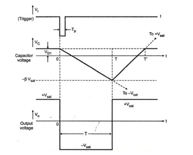
(iv). If VT , a negative trigger of amplitude VT is applied to the non-inverting terminal, so that the effective voltage at this terminal is less than 0.7 V then the output of the Op-amp changes its state from to + Vsat to -Vsat .
(v). The diode is now reverse biased and the capacitor starts charging exponentially to -Vsat through resistance R.
(vi). The voltage at the non-inverting terminal is now -βVsat. When the capacitor voltage becomes just slightly more negative than -βVsat , the output of the Op-amp changes its state back to + Vsat
(vii). The capacitor now starts charging towards + Vsat through R until Vc reaches 0.7V as capacitor gets clamped to the voltage.

Expression for pulse width T
Initial voltage ( at t=0 ) across Capacitor = Vco = VD1
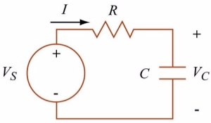
Here Role of supply Voltage will play output voltage Vs = Vo = -Vsat
Voltage across Capacitor at time t is given by the eq
Vc(t) = VD1 e -t/RC + Vo(1 -e -t/RC)
At time t=T
Vo= -Vsat
Vc(T) = - βVsat
Vc(t) = ( VD1 – Vo) e -t/RC + Vo
- βVsat = (VD1 + Vsat ) e -T/RC – Vsat
T = RC ln (1 + VD1 / Vsat ) / 1 - β
β=R2 / R1 + R2
If Vsat >> VD1 and R1 = R2
T= 0.69 RC
For Monostable operation, the trigger pulse width Tp should be much less than T.
The diode D2 is not essential but it is used to avoid malfunctioning if any positive noise spikes are present in triggering line.
It can be seen from the waveform that the voltage Vc does not reach its quiescent value VD1 until time T’>T . Hence it is necessary that a recovery time (T’-T) be allowed to elapse before the next triggering signal is applied.
Q5) Explain astable multivibrator ?
A5)
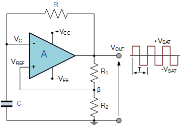
Firstly lets assume that the capacitor is fully discharged and the output of the op-amp is saturated at the positive supply rail. The capacitor, C starts to charge up from the output voltage, Vout through resistor, R at a rate determined by their RC time constant.
In RC circuits that the capacitor wants to charge up fully to the value of Vout (which is +V(sat)) within five time constants. However, as soon as the capacitors charging voltage at the op-amps inverting (-) terminal is equal to or greater than the voltage at the non-inverting terminal,the output will change state and be driven to the opposing negative supply rail.
But the capacitor, which has been charging towards the positive supply rail (+V(sat)), now sees a negative voltage, -V(sat) across its plates. This sudden reversal of the output voltage causes the capacitor to discharge toward the new value of Vout at a rate dictated again by their RC time constant.
Op-amp Multivibrator Voltages
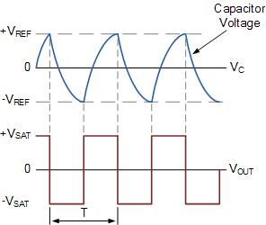
Once the op-amps inverting terminal reaches the new negative reference voltage, -Vref at the non-inverting terminal, the op-amp once again changes state and the output is driven to the opposing supply rail voltage, +V(sat).
The capacitor see’s a positive voltage across its plates and the charging cycle begins again. Thus, the capacitor is constantly charging and discharging creating an astable op-amp multivibrator output.
The period of the output waveform is determined by the RC time constant of the two timing components and the feedback ratio established by the R1, R2 voltage divider network which sets the reference voltage level. If the positive and negative values of the amplifiers saturation voltage have the same magnitude, then t1 = t2 and the expression to give the period of oscillation becomes:
β=R2/ R1 + R2
T = 2 RC x ln(1+β/1-β) since f=1/T
Where: R is Resistance, C is Capacitance, The frequency of oscillation for an Op-amp Multivibrator circuit not only depends upon the RC time constant but also upon the feedback fraction. However, if we used resistor values that gave a feedback fraction of 0.462, (β = 0.462), then the frequency of oscillation of the circuit would be equal to just 1/2RC as shown because the linear log term becomes equal to one.
Q6) An op-amp multivibrator circuit is constructed using the following components. R1 = 35kΩ, R2 = 30kΩ, R = 50kΩ and C = 0.01uF. Calculate the circuits frequency of oscillation.
A6) β=R2/ R1 + R2 = 30K/ 35K + 30K =0.462
T = 2RC ln(1+β/1-β) = 2RC ln (1+0.462/1-0.462)
T = 2 x (50K Ω x 0.01x μF) x ln (2.717)
T = 0.001 x 1 = 0.001 sec or 1 msec
f = 1/T = 1/0.001 = 1,000 Hz or 1kHz
Q7) Explain sequence generator ?
A7)
The sequence generators are nothing but a set of digital circuits which are designed to result in a specific bit sequence at their output. There are several ways in which these circuits can be designed including those which are based on multiplexers and flip flops .
The steps involved during this process are as follows.
Step 1
At first, we need to determine the number of flip-flops which would be required to achieve our objective. In our example, there are 4 states which are identical to the states of a 2-bit counter except the order in which they transit.
Step 2
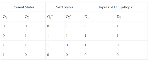
Write the state transition table for our sequence generator. This shown by the first four columns of Table I in which the first two columns indicate the present states while the next two columns indicate the corresponding next states. For instance, first state in our example is 0 = “00” which leads to the next state 1 = “01” .
Step 3
Now this state transition table is to be extended so as to include the excitation table of the flip-flop with which we desire to design our circuit.
In our case, it is nothing but D flip flop due to which we have the fifth and the sixth columns of the table representing the excitation table of D flip-flop.
In Table I in which the present and the next states 1 and 0 (respectively) result in D1 to be 0. The same row also shows the case wherein Qo = Qo + leads to Do=0.
Step 4
Its time to derive the Boolean expressions for D1 and D0. This can be done using any kind of simplification technique including K-map .
However as our example is quite simple, we can just use theBoolean laws to solve for D1 and D0. Thus
D1 =  Qo + Q1 Qo = Qo (
  + Q1) = Qo (1) = Qo
Do = 
 +
+  Qo =
Qo =  (
(  + Qo) =
  (1) =
(1) = 
Step 5:
Now we can design our sequence generator as shown in this figure.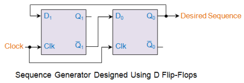
Q8) Explain78 series voltage regulator ?
A8)
A regulated voltage (without fluctuations & noise levels) is very important for the smooth functioning of many digital electronic devices. A common case is with micro controllers, where a smooth regulated input voltage must be supplied for the micro controller to function smoothly.
An example of IC based voltage regulator available in market is the popular 7805 IC which regulates the output voltage at 5 volts.
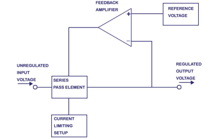
Fixed Voltage Regulators
These regulators provide a constant output voltage. A popular example is the 7805 IC which provides a constant 5 volts output. A fixed voltage regulator can be a positive voltage regulator or a negative voltage regulator.
A positive voltage regulator provides with constant positive output voltage. All those IC’s in the 78XX series are fixed positive voltage regulators. In the IC nomenclature – 78XX ; the part XX denotes the regulated output voltage the IC is designed for. Examples:- 7805, 7806, 7809 etc.
A negative fixed voltage regulator is same as the positive fixed voltage regulator in design, construction & operation.
The only difference is in the polarity of output voltages. These IC’s are designed to provide a negative output voltage. Example:- 7905, 7906 and all those IC’s in the 79XX series.
Q9) Explain LM 317 voltage regulator ?
A9)
LM317 is a 3-terminal regulator IC and it is very simple to use. The IC has 3 pins, in which the input voltage is supplied to pin3 (VIN) then using a pair of resistors (potential divider) we set a voltage at pin 1 (Adjust) which will decide the output voltage of the IC that is given out at pin 2 (VOUT). To make it act as a variable voltage regulator we have to set variable voltages at pin 1 which can be done by using a potentiometer in the potential divider.
The below circuit is designed to take 12V (you can supply up to 24V) as input and regulate it from 1.25V to 10V.
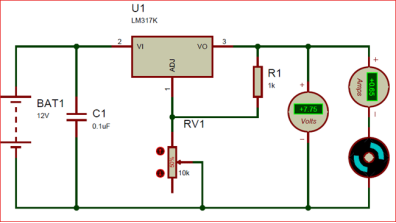
The Resistor R1 (1K) and the potentiometer (10k) together creates a potential difference at adjust pin which regulates the output pin accordingly. The formulae to calculate the Output voltage based on the value of resistors is
VOUT = 1.25 × (1 + (R2/R1))
The value of R1 is 1000 ohms and the value of R2 (potentiometer) is 5000 because it is a 10k potentiometer placed at 50% (50/100 of 1000 is 5000).
Vout = 1.25 × (1 + (5000/1000))
= 1.25 × 6
= 7.5V
And the simulation shows 7.7 V which is pretty much close.
Q10) What are its applications ?
A10)
- Variable power supply
- Current limiting circuits
- Reverse polarity circuits
- Commonly used in Desktop PC, DVD and other consumer products
- Used in motor control circuits