Unit – 3
Combinational Circuits
Using ripple carry adder, this addition is carried out as shown by the following logic diagram-

In the ripple carry adder, the output is known after the carry generated by the previous stage is produced. Thus, the sum of the most significant bit is only available after the carry signal has rippled through the adder from the least significant stage to the most significant stage. As a result, the final sum and carry bits will be valid after a considerable delay
2. What is carry look ahead adder? Define the functions CG and CP.
A carry-look ahead adder (CLA) is a type of adder used in digital logic. It improves speed by reducing the amount of time required to determine carry bits. It can be contrasted with the simpler, but usually slower. The carry-look ahead adder calculates one or more carry bits before the sum, which reduces the wait time to calculate the result of the larger value bits.
The output Gi of the first half-adder is 1if Ai and Bi both are 1 and a carry is generated. The variable Gi is known as ‘Carry Generate’ and can be expressed as:
Gi = Ai Bi
The variable Pi known as ‘Carry Propagate’ because a carry in may be propagated by the full-adder when either or both of the input bits are 1. This condition is expressed as the OR function of A and B:
Pi= A+B
3. What is a Parity Bit?
Parity bit is added to the word containing data in order to make number of 1s either even or odd. Thus it is used to detect errors, during the transmission of binary data .The message containing the data bits along with parity bit is transmitted from transmitter node to receiver node. At the receiving end, the number of 1s in the message is counted and if it doesn’t match with the transmitted one, then it means there is an error in the data.
4. Draw the truth table of an odd parity generator circuit. Realize a circuit to implement the same.
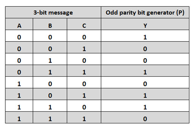
From the truth table, the circuit can be realized as follows:

5. Define a single bit magnitude comparator. Design a 2-bit comparator circuit.
A comparator used to compare two bits, i.e., two numbers each of single bit is called a single bit comparator. It consists of two inputs for allowing two single bit numbers and three outputs to generate less than, equal and greater than comparison outputs.
2 bit comparator:
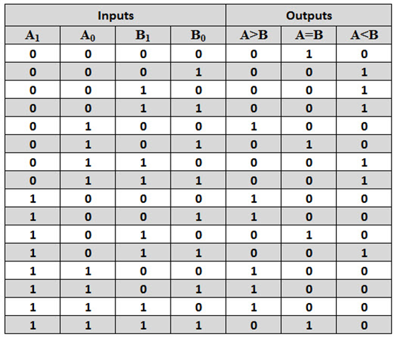
Using K-Maps we get the following equations:
A>B = A1B1′ + B0′ (A0B1′ + A0A1)
A<B = B1A1′ + B0B1A0′ + A1’A0’B0
A=B = 

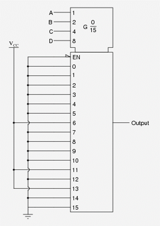
6. Consider the Boolean SOP expression, AB’CD+ABC’D+A’BCD’ for a 16-channel multiplexer. Show the wire connections necessary to make the multiplexer output the specified logic states in response to the data select (A, B, C, and D) inputs.
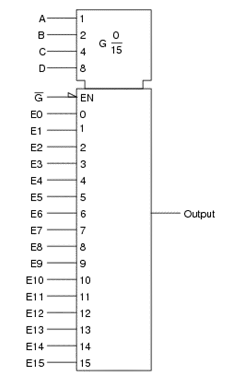
Solution:
The minterms present in the expression should be connected to VCC. Rest of the inputs will be connected to ground.
7. The following schematic diagram is for a two-input selector circuit, which (as the name implies) selects one of two inputs to be sent to the output. Determine what state the “select control” input line has to be in to select input A to be sent to the output, and what state it has to be in to select Input B to go to the output.
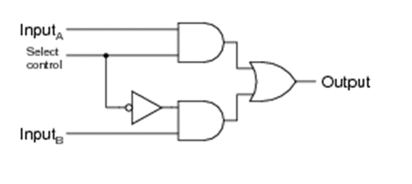
A high signal on the select control line selects Input A , while a low signal on that same line selects Input B.
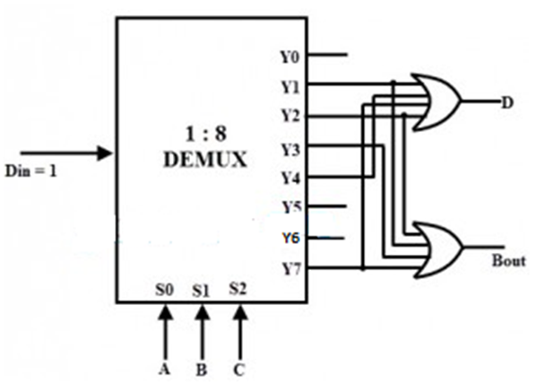
8. What is a demultiplexer? Realize a Full Subtractor circuit using DEMUX.
A demultiplexer is a combinational circuit that performs the opposite function as that of a multiplexer. In a DEMUX, we have n output lines, one input line, and m select lines. The relation between the number of output lines and the number of select lines is the same as we saw in a multiplexer. That is, 2^m = n. Depending on the value of the binary number formed by the select lines, any one of the output lines connects to the input line.
The rest of the output lines at this point go to an OFF state. That is, the value of the remaining lines is 0. In this way, a demultiplexer converts serial data to parallel data and acts as a serial-parallel converter.
9. What are applications of a DEMUX?
10. What is the difference between decoder and demultiplexer?
