Unit 4
Sequential Logic Design
Latches are basic storage elements that operate with signal levels (rather than signal transitions). Latches controlled by a clock transition are flip-flops. Latches are edge-sensitive devices. Latches are useful for the design of the asynchronous sequential circuit.
2. Give a brief description on Clocked SR, JK, MS J-K flip flop, D and T flip-flops?
MS J-K flip flop
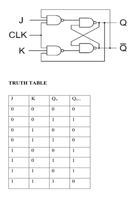
Fig. Master Slave Flip flop
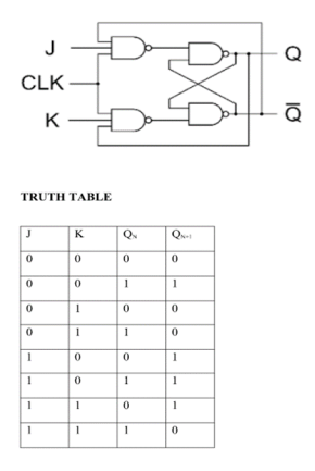
Working of a master slave flip flop –
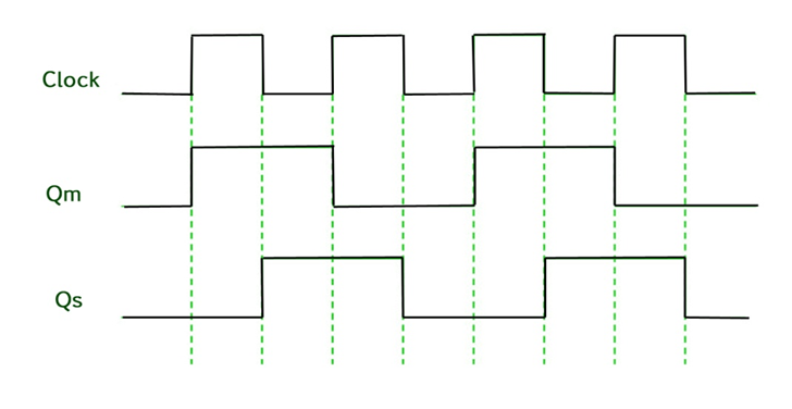
Timing Diagram of a Master flip flop –

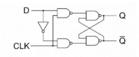
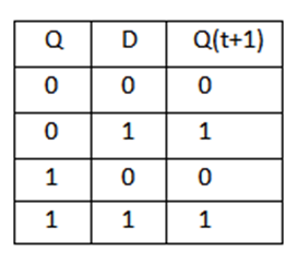
D Flip Flop:
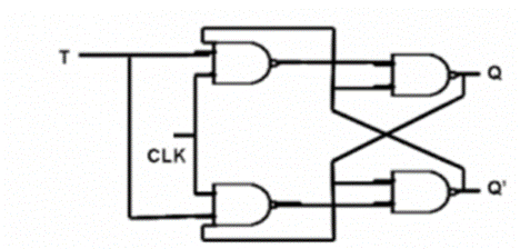
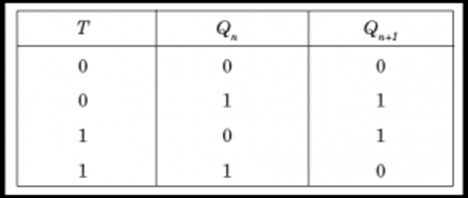
T Flip Flop:
3. What is the use of preset and clear terminals?
Asynchronous inputs on a flip-flop have control over the outputs (Q and not-Q) regardless of clock input status. These inputs are called the preset (PRE) and clear (CLR). The preset input drives the flip-flop to a set state while the clear input drives it to a reset state.
Hold time is defined as the minimum amount of time after the clock's active edge during which data must be stable. Violation in this case may cause incorrect data to be latched, which is known as a hold violation. Note that setup and hold time is measured with respect to the active clock edge only.
Whenever there are setup and hold time violations in any flip-flop, it enters a state where its output is unpredictable: this state is known as metastable state (quasi stable state); at the end of metastable state, the flip-flop settles down to either '1' or '0'. This whole process is known as metastability. In the figure below Tsu is the setup time and Th is the hold time. Whenever the input signal D does not meet the Tsu and Th of the given D flip-flop, metastability occurs.
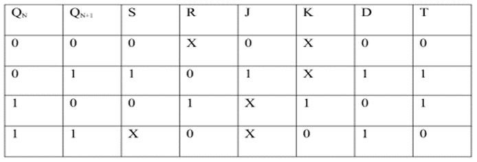
4. Describe in brief about Excitation Table for a flip flop?
EXCITATION TABLE:
Conversion for flip flops:
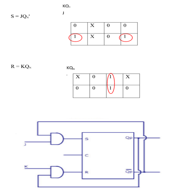
i) SR To JK FlipFlop
Excitation Functions: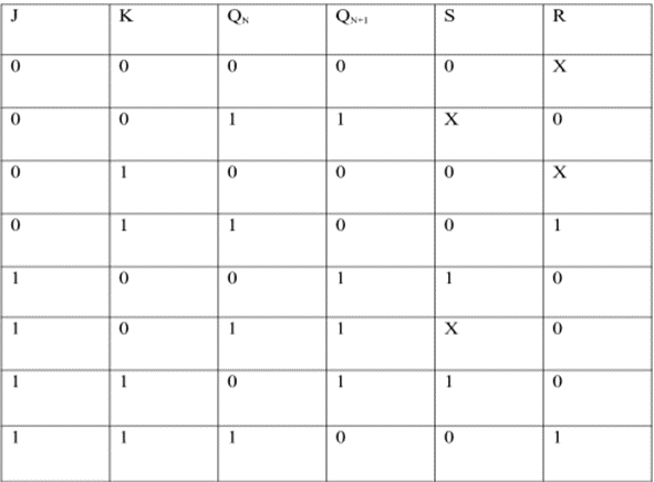
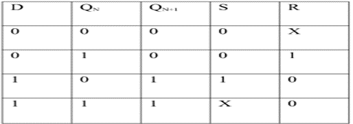
ii) Convert SR To D FlipFlop:
Excitation Functions:
S = DR = D‘

5. Write a brief note on Registers and write its type ?
Flip-flop is a 1 bit memory cell which can be used for storing the digital data. To increase the storage capacity in terms of number of bits, we have to use a group of flip-flop. Such a group of flip-flop is known as a Register. The n-bit register will consist of n number of flip-flop and it is capable of storing an n-bit word.
Shift registers
The registers which shift the bits towards the right are called “Shift right registers”.
Shift registers are of 4 types and they are:
6. Write a short note on Serial-In Serial-Out Shift Register?
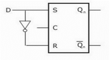
Fig. SISO
Serial-In Parallel-Out shift Register (SIPO) –

Fig. SIPO
7. Write about the function of Parallel-In Serial-Out Shift Register?
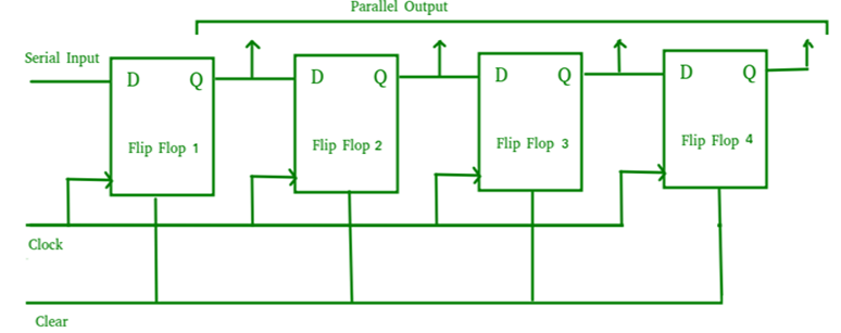
Fig. PISO
Parallel-In Parallel-Out Shift Register (PIPO) –
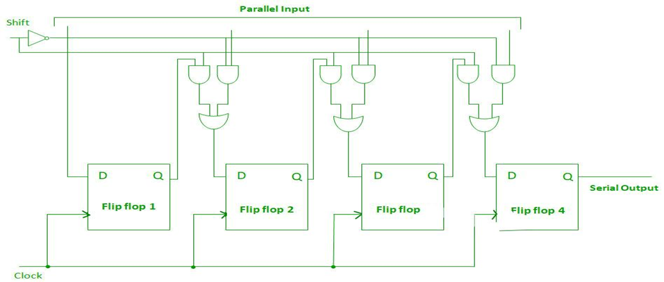
Fig. PIPO
8. What do you mean by Counters?
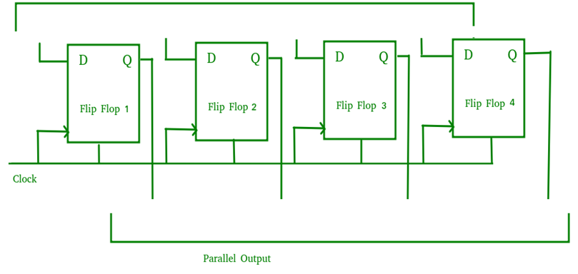

Fig. Ring counter
9. Explain about Ripple counters?
In this universal clock is not used and only the first flip flop is driven by main clock and the clock input of rest of the following is driven by output of previous flip flops.

Fig. Asynchronous counter

Fig. Timing diagram of Asynchronous counter
10. Explain the work of Mod-n counters?
Truth table is as follows:
Clock pulse | Q3 | Q2 | Q1 | Q0 |
0 | 0 | 0 | 0 | 0 |
1 | 0 | 0 | 0 | 1 |
2 | 0 | 0 | 1 | 0 |
3 | 0 | 0 | 1 | 1 |
4 | 0 | 1 | 0 | 0 |
5 | 0 | 1 | 0 | 1 |
6 | 0 | 1 | 1 | 0 |
7 | 0 | 1 | 1 | 1 |
8 | 1 | 0 | 0 | 0 |
9 | 1 | 0 | 0 | 1 |
10 | 0 | 0 | 0 | 0 |
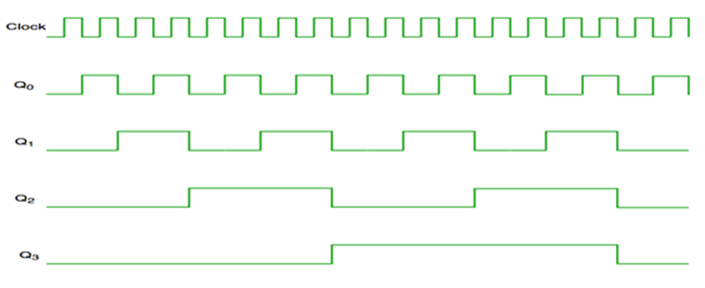
Fig. Decade counter
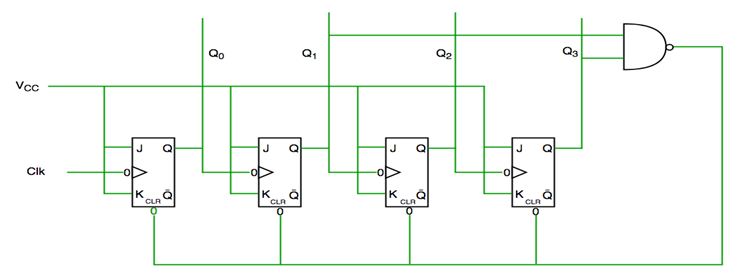
In the above circuit diagram we used nand gate for Q3 and Q1 and sending this to clear input line as the binary representation of 10 is—
1010
And Q3 and Q1 are 1 here, if we give NAND of these two bits then counter clears at 10 and again starts from the beginning.
Up/down counters
Both Synchronous and Asynchronous counters are capable of counting “Up” or counting “Down”, but their is another more “Universal” type of counter that can count in both directions either Up or Down depending on the state of their input control pin and these are known as Bidirectional Counters.
Bidirectional counters, also known as Up/Down counters, are capable of counting in either direction through any given count sequence and they can be reversed at any point within their count sequence by using an additional control input as shown below.
The circuit above is of a simple 3-bit Up/Down synchronous counter using JK flip-flops configured to operate as toggle or T-type flip-flops giving a maximum count of zero (000) to seven (111) and back to zero again. Then the 3-Bit counter advances upward in sequence (0,1,2,3,4,5,6,7) or downwards in reverse sequence (7,6,5,4,3,2,1,0).
Generally most bidirectional counter chips can be made to change their count direction either up or down at any point within their counting sequence. This is achieved by using an additional input pin which determines the direction of the count, either Up or Down and the timing diagram gives an example of the counters operation as this Up/Down input changes state.
Nowadays, both up and down counters are incorporated into single IC that is fully programmable to count in both an “Up” and a “Down” direction from any preset value producing a complete Bidirectional Counter chip. Common chips available are the 74HC190 4-bit BCD decade Up/Down counter, the 74F569 is a fully synchronous Up/Down binary counter and the CMOS 4029 4-bit Synchronous Up/Down counter.
