Unit – 6
Programmable Logic Devices
PLA: Both AND and OR arrays are programmable and Complex, Costlier than PAL.
PAL: AND arrays are programmable OR arrays are fixed, Cheaper and Simpler.
Programmable Array Logic (PAL) is a type of programmable logic device used to realize a particular logical function. PALs comprise of an AND gate array followed by an OR gate array as shown by Figure below. However it is to be noted that here only the AND gate array is programmable unlike the OR gate array which has a fixed logic. This is because here the inputs are fed to the AND gate through fuses (shown in blue), which act as programmable links. Programmable-AND and fixed-OR structure of PALs make them less flexible from programming point of view when compared with Programmable Logic Arrays (PLAs).

2. List the main difference between PROM and PLA.
In some cases the number of don’t care conditions is excessive, it is more economical to use a second type of LSI component called a PLA. A PLA is similar to a ROM in concept; however it does not provide full decoding of the variables and does not generates all the minterms as in the ROM.
3. List the main difference between ROM and RAM.
RAM is Random Access Memory. It is a random access read/write memory. The data can be read or written into any selected address. RAMs are called as Volatile memories because RAMs lose stored data when the power is turned OFF. ROM is a type of memory in which data are stored permanently or semi permanently. Data can be read from a ROM, but there is no write operation. ROMs are called as Non-Volatile memories because ROMs doesn’t lose stored data when the power is turned OFF.
4. Write a short note on DRAM
DRAM stores data by writing a charge to the capacitor by way of an access transistor. DRAM looks at the state of charge in a transistor-capacitor circuit ; a charged state is a 1 bit; the low charge is seen as a 0 bit.
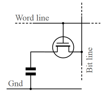
DRAM uses capacitors that lose charge over time due to leakage, even if the supply voltage is maintained. Since the charge on a capacitor decays when a voltage is removed, DRAM must be supplied with a voltage to retain memory (and is thus volatile). Capacitors can lose their charge a bit even when supplied with voltage if they have devices nearby (like transistors) that draw a little current even if they are in an “off” state; this is called capacitor leakage. Due to capacitor leakage, DRAM needs to be refreshed often.
5. Write a short note on SRAM
SRAM does not use capacitors. SRAM uses several transistors in a cross-coupled flip-flop configuration and does not have the leakage issue and does not need to be refreshed.
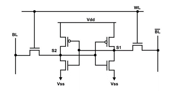
Figure above shows SRAM with 6 transistors. But SRAM still needs constant power to maintain the state of charge and thus is volatile like DRAM. Since SRAM uses several transistors per bit of memory versus DRAM, which uses one transistor and capacitor per bit, DRAM is less expensive. SRAM is faster and typically used for cache, DRAM is less expensive and has a higher density and has a primary use as main processor memory.
6. What is PLD?
A programmable logic device is an electronic component used to build reconfigurable digital circuits. Unlike a logic gate, which has a fixed function, a PLD has an undefined function at the time of manufacture.
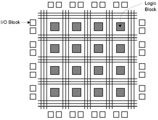
7. Summarize about FPGA with the help of a neat diagram of its architecture.
• A field‐programmable gate array (FPGA) is a VLSI circuit that can be programmed at the user’s location.
• A typical FPGA consists of an array of millions of logic blocks, surrounded by programmable input and output blocks and connected together via programmable interconnections.
• A typical FPGA logic block consists of lookup tables, multiplexers, gates, and flip‐flops. A lookup table is a truth table stored in an SRAM and provides the combinational circuit functions for the logic block.
8. Why the input variables to a PAL are buffered.
The input variables to a PAL are buffered to prevent loading by the large number of AND gate inputs to which available or its complement can be connected.
9. Implement the functions given below using PLA
F1 (A, B, C) = (0, 1, 3, 4)
F2 (A, B, C) = (1, 2, 3, 4, 5)
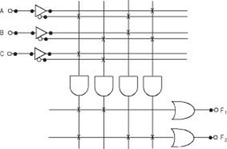
Assume that a 3 × 4 × 2 PLA is available for the realization of the above functions. It should be noted that according to the number of inputs and output, the specified PLA is sufficient to realize the functions. However, total distinct minterms in the functions are six, whereas available product terms or the number of AND gates in the specified PLA is four. So some simplification or minimization is required for the functions.
The simplified equations obtained from the K-Maps are:
F1 =B’C’ +A’C
F2 =A’B +A’C +AB’
In these expressions, there are four distinct product terms-B'C', A'C, A'B, and AB'. So these functions can be realized by the specified 3 × 4 × 2 PLA. The internal connection diagram for the functions using PLA after fuse-links programming can be drawn as:
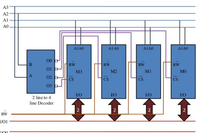
10. Obtain a 16x2 memory using 4x2 memory IC’s
Number of chips required= 16/4=4
At any one time, only one of the 16 locations is to be accessed, which will be in one of the four chips. This means only one of the four chips must get selected at a time.
For selecting one out of 16 locations, the number of address lines required is 4 (24 = 16). The address lines A0 and A1 will be same for each chip, and the address lines A2- A3 must select one out of the four chips. For this purpose, a 2-line to 4 –line decoder is used. The memory connections are shown below:
