Unit 1
MOSFET and its Analysis
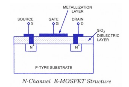
Figure shows the construction of an N-channel E-MOSFET. The main difference between the construction of Depletion -MOSFET and that of Enhancement -MOSFET, as we see from the figures given below the E-MOSFET substrate extends all the way to the silicon dioxide (SiO2) and no channels are doped between the source and the drain. Channels are electrically induced in these MOSFETs, when a positive gate-source voltage VGS is applied to it.
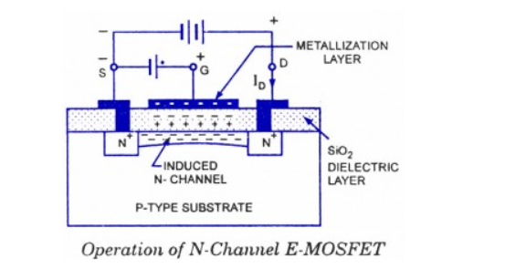
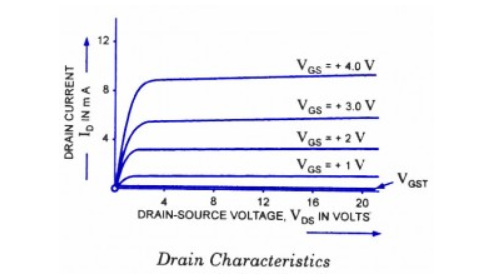
For VGS below VGST, the drain current ID = 0. But for VGS exceeding VGST an N-type inversion layer connects the source to drain and the drain current ID is large.
2. Explain its characteristics?
Characteristics
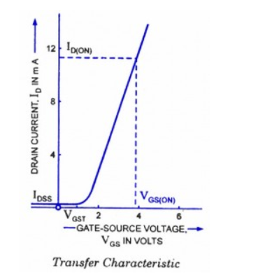
The figure shows the transfer characteristics of E-MOSFET
The equation for the transfer characteristic of E-MOSFETs is given as:
ID=K(VGS-VGST)2
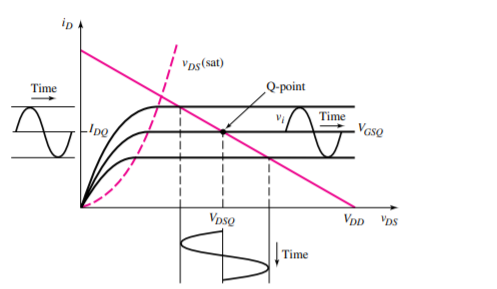
3. Explain the DC load line characteristics?
1.1.1 DC Load line
4. Explain the AC equivalent circuit?
AC equivalent circuit
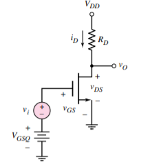
From the figure we see that the output voltage is
vDS = vo = VDD -iD RD -----------------------------------(1)
Using eq(1) we obtain
vo = VDD – (IDQ +id) RD = (VDD – IDQ RD) - idRD----------------------------(2)
The output voltage is a combination of dc and ac value . The time-varying output is the time-varying drain-to-source voltage or
Vo = vds = -idRD------------------------------------------------------(3)
We know that
id = gm vgs --------------------------------------------------------------------(4)
The equations in terms of instantaneous ac values as well as the phasors are
vgs=vi
or
Vgs = Vi
And
id = gm vgs
and
vds = -id RD
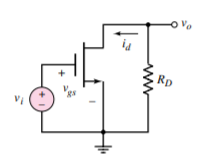
AC equivalent circuit
The ac equivalent in figure is developed by setting the dc sources in figure is equal to zero.
5. Explain its parameters?
The instantaneous gate to source voltage is
vGS= VGSQ + vi = VGSQ + vgs------------------------------------(1)
where VGSQ is the dc component and vgs is the ac component. The instantaneous drain current is
iD = Kn(vGS – VTN) 2-----------------------------------------------------(2)
Substituting (1) in (2) we get
iD= Kn[VGSQ + vgs -VTN ] 2 = Kn [(VGSQ – VTN +vgs] 2---------------------(3a)
or
iD= Kn[VGSQ -VTN ] 2 +2Kn [(VGSQ – VTN ) vgs + Kn v2 gs ----------------------------(3b)
The first term in (3b) is the dc or quiescent drain current IDQ , The second term is the time-varying drain current component that is linearly related to the signal vgs and the third term is proportional to the square of the signal voltage.
For sinusoidal input signal the squared term produces undesirable harmonics or non-linear distortion in the output voltage.
To minimize these harmonics we require
vgs ≤ 2(VGSQ- VTN )
6. What is parasitic?
Due to their structure, MOSFETs have a parasitic capacitance, as indicated in the diagram below. The diagram below is for an example of an N-channel MOSFET, but the situation is much the same for P-channel devices.
In the power MOSFETs we handle large amounts of power, the parasitic capacitance must be regarded as a parameter that limits the usage frequency and switching speed.
The drain and source of a MOSFET are insulated from the gate by the gate oxide film. A PN junction is formed between the drain and source with substrate intervening, and a parasitic ("body") diode is present.
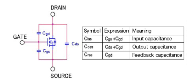
The three parameters Ciss, Coss, Crss appearing on MOSFET data sheets in general relate to these parasitic capacitances.
Ciss is the input capacitance, and is the capacitance obtained by totaling the gate-source capacitance Cgs and the gate-drain capacitance Cgd; it is the capacitance of the MOSFET as a whole, as seen from the input. Qg is the amount of charge necessary to drive (charge) Ciss.
Coss is the output capacitance, obtained by adding the drain-source capacitance Cds and the gate-drain capacitance Cgs, and is the total capacitance on the output side.
If Coss is large, a current arising due to Coss flows at the output even when the gate is turned off, and time is required for the output to turn off completely.
Crss is the gate-drain capacitance Cgd itself, and is called the feedback capacitance or the reverse transfer capacitance.
If Crss is large, the rise in drain current is delayed even after the gate is turned on, and the fall in current is delayed after the gate is turned off.
In other words, this parameter greatly affects switching speed. Qgd is the charge amount necessary to drive (charge) Crss.
7. Explain the non-ideal characteristics?
Finite output resistance:
Due to channel -length modulation the MOSFET drain current is slightly dependent on vDS and thus is defined as
iD = K(vGS – Vt) 2 (1+  vDS)
vDS)
To determine the relationship between the small signal voltage vgs and small signal current id we can apply small signal analysis of this equation as
id = d iD / d vGS | vGS= VGS
= 2K (vGS – Vt) | VGS = VGS vgs
= 2K (vGS – Vt). Vgs
= gm.vgs
v DS and current iD are related by
id = d iD / d vGS | vGS= VGS .Vds
=  K (Vgs – VT) 2 |vGS= VGS .Vds
= v ds / ro
ro = output resistance
Body effect
The body effect occurs in MOSFET in which the substrate or body is not connected to the source. For an NMOS device the body is connected to the most negative potential in the circuit and will be at signal ground.
The simplified current-voltage relation is
iD = Kn (vGS– VTN )2 and the threshold is given by
VTN = VTNO + [
[  2ɸ +vsB -
  2ɸf ]
2ɸf ]
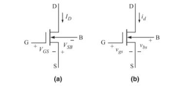
Sub Threshold Construction
In order to address the subthreshold conduction phenomenon let us plot the
IDS-VGS characteristics shown in Figure below.
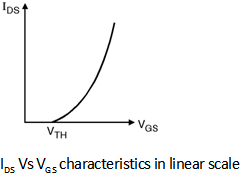
A closer inspection of the IDS-VGS curve shows that the current does not drop abruptly to '0' at VGS = VTH.
It indicates that the MOS transistor is partially conducting for voltages below the threshold voltage.
This effect is called as subthreshold or weak inversion conduction.
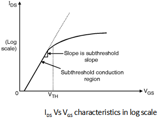
From the IDS-VGS curve in log scale it is clear that current does not drop to zero immediately for VGS < VTH but actually decays in an exponential fashion.
Thus even VGS < VTH IDS is finite but it exhibits exponential dependence on VGS for smaller values of VDS roughly in the range of 200 mV.
The subthreshold conduction effect can be formulated as :
IDS = I0 exp VGSnKTq
Where n > 1 is a non ideality factor.
• In digital circuit designs the presence of subthreshold current is not desirable because it deviates the transistor from its ideal switch like behaviour which require that current should drop as fast as possible once the gate to source voltage falls below VTH.
• The subthreshold conduction behaviour is represented subthreshold slope factor (S) which indicates the change in VGS for one decaded change in drain current. The unit of S is mV/decade.
• From the above Equation we can show that,
S = n KTq ln (10)
Temperature Effect
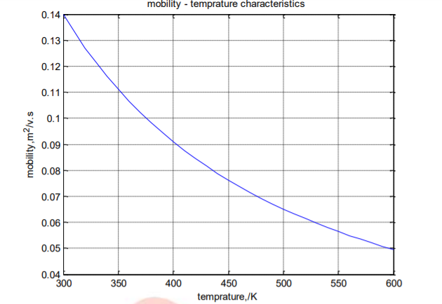
In order to capture the dependence of mobility on temperature , doping, and electric field different mathematical models were developed. The carrier mobility is given by
μT = μ (Tr) (T/Tr) k μ
where
T = Absolute temperature
Tr = Room temperature
Kμ = Fitting parameter with a typical value of about 1.5
μ(Tr)= ref temp (300K) = 0.14 m2 / v.s
The analytical modelling of the carrier mobility is shown in figure. It reveals the inverse relationship between temperature and carrier mobility .
Effect of W/L ratio
The K constant specifically Kn is called the conduction parameter of the n-channel device.
Kn is given by:
Kn=k′n/2⋅W/L
Where
k′n=μnCox
μn is the mobility of the electrons in the inversion layer and Cox is the oxide capacitance per unit area.
According to Neamen the k′n parameter is called the "process conduction parameter" and is considered to be a constant for a fabrication technology. Therefore, the ratio W/L is the transistor design variable.
Neamen goes on to say that the design variable is used to design MOSFETS to produce specific current-voltage characteristics in MOSFET circuits.
8. Explain common source amplifier ?
Figure below shows the common source amplifier circuit. In this circuit the MOSFET converts variations in the gate-source voltage into a small signal drain current which passes through a resistive load and generates the amplified voltage across the load resistor.
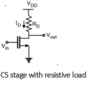
Now from above Figure,
ID = ½ μ Cox W/L (VGS – VTH )2
That is
ID = ½ μ Cox W/L (Vin – VTH )2
By KVL
VDD – ID RD = Vout
Vout = VDD– ½ μn Cox W/L (Vin – VTH )2RD
Differentiating this equation with respect to Vin
dVout / dVin = - μn Cox W/L (Vin – VTH )RD
Hence the voltage gain Av = -gmRD
Also, from small signal model of shown in above Figure.
By applying KVL,
Vin – VGS = 0
Vin = VGS
Also,
Vout + gmVGSRD =0
Vout = -gmVGS RD
Hence, the voltage gain Av = Vout / Vin – gm RD
As the gate terminal of MOSFET draws a zero current we can say that the common source amplifier provides a current gain of infinity.
Therefore Ai= ∞
Also because of zero gate current the input impedance of CS amplifier is also infinite. Therefore, Rin = ∞
In order to calculate the output impedance Rout consider the circuit shown in
Figure below.
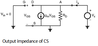
By applying KCL at point 'A'
We get
gmVGS + Vx-0/RD = Ix
But VGS =0
Vx/RD = Ix
Rout = Vx/Ix = RD
Rout = RD
The output impedance of common source amplifier is
Rout = RD
9. Explain source follower?
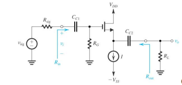
This is the common drain amplifier. This type of amplifier has the input signal fed at the gate similar to the CS amplifier but the signal output is taken at the source terminal as shown in figure.
We’ll calculate the following small-signal quantities for this MOSFET common gate amplifier Rin, Av, Avo, Gv, Gi , Ais and Rout. To begin construct the small-signal equivalent circuit:
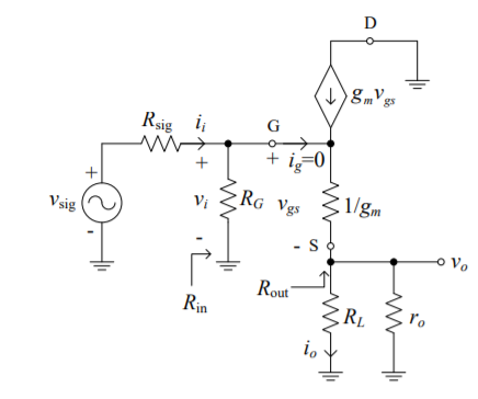
Because the drain terminal is an AC ground, one end of the output resistance ro was shifted so it appears in parallel with RL. This makes the T model suited for amplifier since RL || ro appears series with 1/gm.
Input resistance Rin : With ig =0 the small signal equivalent circuit that
Rin = RG .
Partial small signal voltage gains Av and Avo. At the output side of the small signal circuit with ig=0
vo = gm vgs (RL ||ro )
At the input using voltage division
vgs = 1/gm/ 1/gm + RL ||ro . vi
The small signal partial voltage gain
Av = vo/vi = RL ||ro / RL || ro + 1/gm
Notice that if ro>> RL and RL>> 1/gm then AV< 1
In case of open circuit load (RL ∞) the small-signal partial voltage gain becomes
Avo = Av|RL ->∞ =ro/ ro + 1/gm
Overall small signal voltage gain G . Using voltage division at the input to the small -signal equivalent circuit
vi = Rin / Rin + Rsig. Vsig
Substituting this
Gv = vo/vsig = Vi/vsig. Vo/vi = vi/vsig . Av
The overall small signal voltage gain of this common drain amplifier to be
Gv = vo/vsig = RG/ RG + Rsig . RL ||ro / RL ||ro + 1/gm
If ro>> RL and RL>> 1/gm as well as RG >>Rsig then
Gv< 1
This common drain amplifier is called source follower amplifier.
10. Explain the frequency response of amplifier?
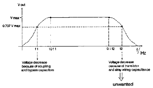
Figure shows the typical frequency response of an amplifier. At low frequencies the output voltage decreases because of coupling and bypass capacitors. At high frequencies, the output voltage decreases because of transistor and stray wiring capacitance.
Critical frequencies:
Where the output voltage is 0.707 of Vmax.
Two critical frequencies -> f1, f2
Midband:
Is the band of frequencies between 10 * f1 and 0.1 * f2.
The midband is where an amplifier is supposed to be operated.
Ex: Find the midband of an amplifier with f1 = 5 Hz and f2 = 100 KHz.
10 * f1 = 10 * 5 Hz = 50 Hz -- > lower end
0.1 * f2 = 0.1 * 100 KHz = 10 KHz -- > upper end
Midband: 50 Hz - 10 KHz