Unit 2
MOSFET Circuits
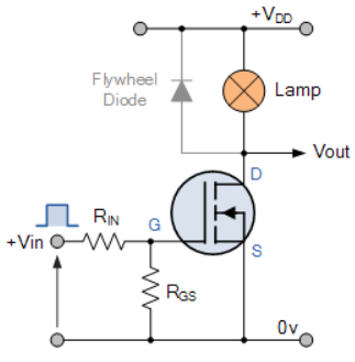
In this circuit arrangement an Enhancement-mode N-channel MOSFET is being used to switch a simple lamp “ON” and “OFF”.
The gate input voltage VGS is taken to an appropriate positive voltage level to turn the device and therefore the lamp load either “ON”, ( VGS = +ve ) or at a zero voltage level that turns the device “OFF”, ( VGS = 0V ).
If the resistive load of the lamp was to be replaced by an inductive load such as a coil, solenoid or relay a “flywheel diode” would be required in parallel with the load to protect the MOSFET from any self- generated back-emf.
The simple circuit for switching a resistive load such as a lamp or LED. But when using power MOSFETs to switch either inductive or capacitive loads some form of protection is required to prevent the MOSFET device from becoming damaged. Driving an inductive load has the opposite effect from driving a capacitive load.
For example, a capacitor without an electrical charge is a short circuit, resulting in a high “inrush” of current and when we remove the voltage from an inductive load we have a large reverse voltage build up as the magnetic field collapses, resulting in an induced back-emf in the windings of the inductor.
2. Explain CMOS inverter?
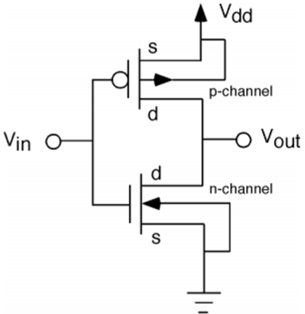
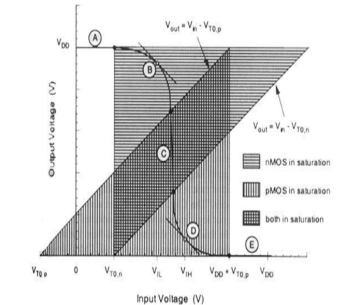
The CMOS inverter circuit is shown in the figure. Here, nMOS and pMOS transistors work as driver transistors; when one transistor is ON, other is OFF.
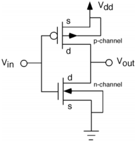
This configuration is called complementary MOS (CMOS). The input is connected to the gate terminal of both the transistors such that both can be driven directly with input voltages. Substrate of the nMOS is connected to the ground and substrate of the pMOS is connected to the power supply, VDD.
So VSB = 0 for both the transistors.
V_{GS,n}=V_{in}
V_{DS,n}=V_{out}
And,
V_{GS,p}=V_{in}-V_{DD}
V_{DS,p}=V_{out}-V_{DD}
When the input of nMOS is smaller than the threshold voltage (Vin <VTO,n), the nMOS is cut – off and pMOS is in linear region. So, the drain current of both the transistors is zero.
I_{D,n}=I_{D,p}=0
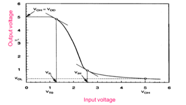
Therefore, the output voltage VOH is equal to the supply voltage.
V_{out}=V_{OH}=V_{DD}
When the input voltage is greater than the VDD + VTO,p, the pMOS transistor is in the cutoff region and the nMOS is in the linear region, so the drain current of both the transistors is zero.
I_{D,n}=I_{D,p}=0
Therefore, the output voltage VOL is equal to zero.
V_{out}=V_{OL}=0
The nMOS operates in the saturation region if Vin > VTO and if following conditions are satisfied.
V_{DS,n}\geq V_{GS,n}-V_{TO,n}
V_{out}\geq V_{in}-V_{TO,n}
The pMOS operates in the saturation region if Vin < VDD + VTO,p and if following conditions are satisfied.
V_{DS,p}\leq V_{GS,p}-V_{TO,p}
V_{out}\leq V_{in}-V_{TO,p}
3. Explain resistive load inverter ?
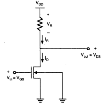
The basic structure of a resistive load inverter is shown in the figure given below. Here, enhancement type nMOS acts as the driver transistor. The load consists of a simple linear resistor RL. The power supply of the circuit is VDD and the drain current ID is equal to the load current IR.
Circuit Operation
When the input of the driver transistor is less than threshold voltage VTH (Vin < VTH), driver transistor is in the cut – off region and does not conduct any current. So, the voltage drop across the load resistor is ZERO and output voltage is equal to the VDD.
Now, when the input voltage increases further, driver transistor will start conducting the non-zero current and nMOS goes in saturation region.
4. Explain current sink and source?

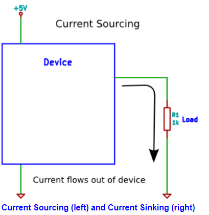
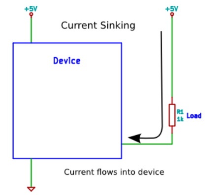
The load in the circuit diagram is shown as a 1k resistor, but can be any load that draws a current such as an LED and series resistor, the coil of a relay, a light bulb, etc.
The device in the circuit diagram can be any electronic circuit or device such as a microcontroller, FPGA, CPLD, logic circuit, etc.
Current Sourcing:
When a load is connected to a device so that the device supplies current to the load (sources current) then the configuration is said to be current sourcing.
An example is a series resistor and LED connected between a microcontroller pin and GND. When the microcontroller pin is switched high (logic 1) then the microcontroller will source current to the load. In this configuration a logic 1 will supply power to the load (switch the LED on) and a logic 0 will switch power to the load off (switch the LED off).
Current Sinking
When a load is connected to a device so that current flows from the power supply through the load and into the device, then the configuration is said to be current sinking. When current flows into the device, it is said to be sinking current.
An example of current sinking is when a series resistor and LED is connected between power (e.g. +5V) and a microcontroller pin. When the microcontroller pin is switched high (logic 1) then the current to the load is switched off. When the microcontroller switches the pin low (logic 0), current flows through the load.
5. Explain current mirror?
The calculation of the current gain n starts with the expressions of the input and of the output currents.
Iin = ID1 = β1(VGS 1 – VTh1 ) 2 ( 1 +  VDS1)
VDS1)
Iout = ID2 = β2 (VGS2 – VTh2 )2 ( 1+ 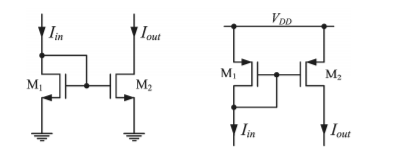 VDS2)
VDS2)
β 1 = μ Cox W1/ 2 L1β2 = μ Cox W2 / 2 L2
If the gate-source voltages of the transistors are assumed to be equal, the current gain results
n = Iout/Iin = β2 (VGS2 – VTh2 )2 ( 1+  VDS2) / β1 (VGS2 – VTh2 ) 2 ( 1+
  VDS1)
VDS1)
The input resistance of the mirror can be determined from the small signal equivalent model. First the input voltage is written as a function of the input current:
Vin = (Iin -I1 ) rDS1 = (Iin – gm VGS1 ) rDS1
The gate-source voltage VGS1 of the transistor M1 can be identified from the schematic as the input voltage.
By replacing VGS1 with Vin in the equation (4) the input resistance results:
Rin = Vin / Iin = rDS1/ 1+gm1 rDS1 = 1/ gm1
The output resistance can be calculated with a similar method as for a simple, one transistor current source.
The final expression of the output resistance is 1 out DS out
Rout = Vout/Iout = rDS1
6. Explain the four types of feedback amplifier?
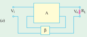
Voltage series:
It is also called shunt derived series-fed feedback. The amplifier and the feedback circuit are connected series parallel. Here a fraction of the output voltage is applied in series with the input voltage via the feedback.
The output resistance of the amplifier is reduced by the shunting effect of the input to the feedback network.
Ro’ = Ro/ (1+β A)
Similarly, Vi sees two circuit elements in series:
(i) The input resistance of the amplifier
(ii) The output resistance of the feedback network.
Hence, input resistance of the amplifier as a whole is increased due to feedback.
Ri’ = Ri (1+βA)
The series feedback always increases the input impedance by a factor of (1+βA)

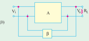
Voltage shunt

It is also known as shunt-derived shunt-fed feedback that is it is parallel-parallel prototype. A small portion of the output voltage is coupled back to the input voltage parallel.
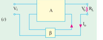
Current series feedback :
It is also known as series-derived series-fed feedback. Here, a part of the output current is made to feedback a proportional voltage in series with the input. Since it is a series pick up and series feedback both the input and output impedances of the amplifier are increased due to feedback.
Current shunt feedback
It is referred to as series-derived shunt-fed feedback. It is a parallel-series (PS) prototype. Here, the feedback network picks up a part of the output current and develops a feedback voltage in parallel with the input voltage.
The feedback network shunts the input but is in series with the output. Hence, output resistance of the amplifier is increased whereas its input resistance is decreased by a factor of loop gain.
7. Explain the effects of feedback ?
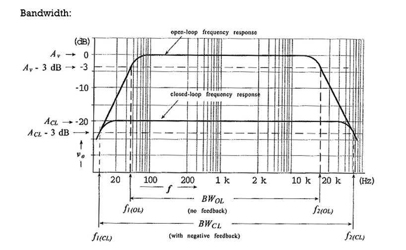
Effects of Negative Feedback in Amplifiers can be measured in decibels. A statement that 40 dB of feedback has been applied to an amplifier means that the amplifier gain has been reduced by 40 dB. Thus,
ACL = Av -40dB = Av/100
Consider the typical gain-frequency response of an amplifier, as illustrated in Fig. Without negative feedback, the amplifier open-loop (Av) gain falls off to its lower 3 dB frequency (f1(OL)), as illustrated.
This is usually due to the impedance of bypass capacitors increasing as the frequency decreases.
Similarly, the open-loop upper cut-off frequency (f2(OL)) is produced by transistor cut-off, by shunting capacitance, or by a combination of both.
BW OL = f2 (OL) – f1(OL)
The closed-loop gain (ACL) is much smaller than the open-loop gain, and ACL does not begin to fall off (at high or low frequencies) until Av (open-loop) falls substantially.
Consequently, f1(CL) is much lower than f1(OL), and f2(OL) is much higher than f2(OL). So, the circuit bandwidth with negative feedback (the closed-loop bandwidth) is much greater than the bandwidth without negative feedback.
BW CL = f2(CL) – f1 (CL)
ACL = Av/ 1+Av B
From Eq.
It can be shown that there is a 90° phase shift associated with the open-loop gain at frequencies below f1(OL) and above f2(OL).
ACL = -jAv/ 1-jAvB
| ACL | = Av /  [ 1 + (Av B) 2 ]
When Av = 1/B,
| ACL | = 1/B /  [ 1 + 1 ] = ACL /
= ACL – 3 dB
Thus, for a Effects of Negative Feedback in Amplifiers designed to have the widest possible bandwidth, the cutoff frequencies would occur when the open-loop gain falls to the equivalent of 1/B. Thus, f2(CL) occurs when,
Av = 1/ B ͌ ACL
So, for example, the cutoff frequencies for a negative feedback amplifier designed for a closed-loop gain of 100 would occur when the open-loop gain falls to 100. It is seen that,
negative feedback increases amplifier bandwidth.
The upper cut-off frequency for an amplifier is usually greater than 20 kHz, and the lower cut-off frequency is around 100 Hz, or lower. So, f2 ≫ f1, and consequently,
BW = f2 – f1 ͌ f2
This means that the amplifier bandwidth is essentially equal to the upper cut-off frequency.
The amplifier gain multiplied by the upper cut-off frequency is a constant quantity. This is known as the gain-bandwidth product. Therefore,
ACL x f2(CL) = Av x f1 (OL)
f 2(CL) = Av f1(OL)/ ACL
So, the closed-loop upper cut-off frequency for a negative feedback amplifier can be calculated from the open-loop upper cut-off frequency, the open-loop gain, and the closed-loop gain
8. Explain voltage feedback amplifier analysis ?
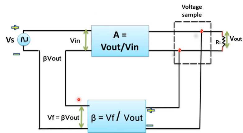
Voltage series feedback increase input impedance of the amplifier. Because back signal return to input in series to oppose the applied voltage causing input current fall and impedance increase.
Output signal = voltage signal
Feedback signal = voltage signal
Shun driven series fed feedback is given by
Ii = Vi/Zi = Vs -Vf / Zi = Vs – βVo / Zi
Ii = Vs – β A Vi / Zi
Ii . Zi = Vs – β A Vi
Vs = Ii Zi + β A Vi = Ii Zi + βA Ii Zi
Zif = Vs/Ii = Zi (β A) Zi
= Zi(1+βA)
9. Explain current series feedback amplifier?
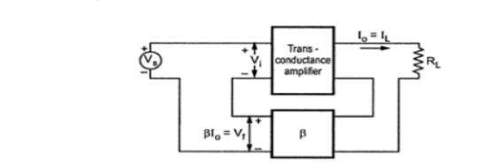
Current series feedback amplifier:
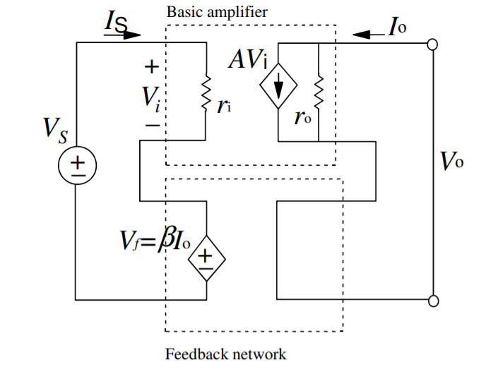
Voltage gain
Io = A. Vi = A (Vs-Vf)
Vf = β . Io
A(Vs – βIo) = Io
AVs = (1+β A) Io
Af = Io /Vs = A / (1+βA)
Input Impedance:
Zin = Vs/Is = Vi + Vf / Is
= Vi + β Vo /Is
= Vi + β A Vi /Is
= Vi(1+βA)/Is
= ri(1+βA)
Output Impedance:
Zout IVs=0 ;
Io = Vo – A . Vi/ro
Vi + Vf = Vs =0
Io = Vo + A.β.Io/ ro
Zout = Vo/Io = ro/ 1 + A β
10. Explain Barkhausen criteria?
Conditions which are required to be satisfied to operate the circuit as an oscillator are called as “Barkhausen criterion” for sustained oscillations.
The Barkhausen criteria should be satisfied by an amplifier with positive feedback to ensure the sustained oscillations.
For an oscillation circuit, there is no input signal “Vs”, hence the feedback signal Vf itself should be sufficient to maintain the oscillations.
The Barkhausen criterion states that:
• The loop gain is equal to unity in absolute magnitude, that is, | β A | = 1 and
• The phase shift around the loop is zero or an integer multiple of 2π: ∠β A = 2 π n, n ∈ 0, 1, 2,….
The product β A is called as the “loop gain”.
11. Explain Wein bridge oscillator?
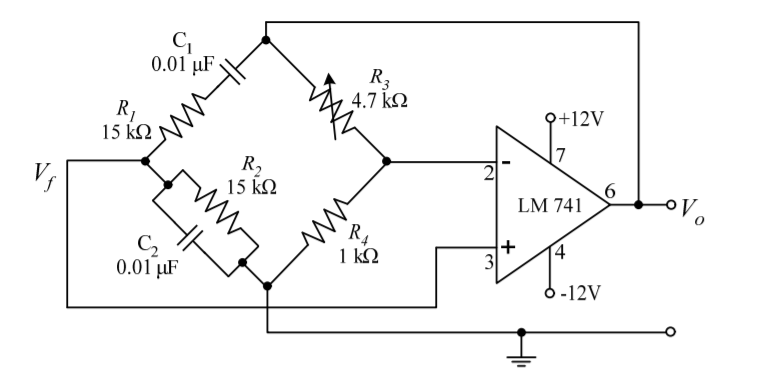
Wien bridge oscillator is an audio frequency sine wave oscillator of high stability and simplicity. The feedback signal in this circuit is connected to the non-inverting input terminal so that the op-amp is working as a non-inverting amplifier.
The feedback network does not provide any phase shift. The circuit can be viewed as a Wien bridge with a series combination of R1 and C1 in one arm and parallel combination of R2 and C2 in the adjoining arm. Resistors R3 and R4 are connected in the remaining two arms.
The condition of zero phase shift around the circuit is achieved by balancing the bridge. The series and parallel combination of RC network form a lead-lag circuit.
At high frequencies, the reactance of capacitor C1 and C2 approaches zero. This causes C1 and C2 appears short. Here, capacitor C2 shorts the resistor R2. Hence, the output voltage Vo will be zero since output is taken across R2 and C2 combination. So, at high frequencies, circuit acts as a 'lag circuit'.
At low frequencies, both capacitors act as open because capacitor offers very high reactance. Again, output voltage will be zero because the input signal is dropped across the R1 and C1 combination. Here, the circuit acts like a 'lead circuit'.
But at one particular frequency between the two extremes, the output voltage reaches to the maximum value. At this frequency only, resistance value becomes equal to capacitive reactance and gives maximum output. Hence, this frequency is known as oscillating frequency (f).

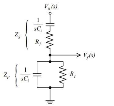
Consider the feedback circuit, on applying voltage divider rule
Vf(s) = Vo(s) x Zp(s)/ Zp(s) + Zs(s)
Zs(s) = R1 + 1/sC1 and Zp(s) = R2|| 1/sC2
Let R1=R2=R and C1=C2=C . On solving
β = Vf(s)/ Vo(s) = RsC /(RsC) 2 + 3RsC + 1 ---------------------------(1)
Since the op-amp is operated in the non-inverting configuration the voltage gain
Av = Vo(s)/ Vf(s) = 1 + R3/R4 -------------------(2)
Applying the condition for sustained oscillations, = Av β =1
RsC /(RsC) 2 + 3RsC + 1. 1 + R3/R4
S=jw
(1 + R3/R4) ( jwRC/ - R2 C2 w2 + 3 jwRC + 1) =1
jw RC (1 + R3/R4)= (- R2 C2 w2 + 3 jwRC + 1)
jw[(1 + R3/R4)RC – 3RC] = 1- R2 C2 w2
To obtain the frequency of oscillation equate the real part to zero
1- R2 C2 w2 = 0
w = 1/RC
f = 1/ 2 π RC
To obtain the condition for gain at the frequency of oscillation equate the imaginary part to zero.
jw[(1 + R3/R4)RC – 3RC] = 0
jw[(1 + R3/R4)RC= jw3RC
[(1 + R3/R4) =3
R3/R4 =2
Therefore R3 = 2 R4 is the required condition.
12. Explain phase shift oscillator?
Phase Shift oscillator
In an RC Oscillator circuit, the input is shifted 180o through the feedback circuit returning the signal out-of-phase and 180o again through an inverting amplifier stage to produces the required positive feedback.
This then gives us “180o + 180o = 360o” of phase shift which is effectively the same as 0o, thereby giving us the required positive feedback.
In other words, the total phase shift of the feedback loop should be “0” or any multiple of 360o to obtain the same effect.
The circuit on the left shows a single resistor-capacitor network whose output voltage “leads” the input voltage by some angle less than 90o.
In a pure or ideal single-pole RC network. it would produce a maximum phase shift of exactly 90o, and because 180o of phase shift is required for oscillation, at least two single-poles networks must be used within an RC oscillator design.
However, in reality it is difficult to obtain exactly 90o of phase shift for each RC stage so we must therefore use more RC stages cascaded together to obtain the required value at the oscillation frequency.
The amount of actual phase shift in the circuit depends upon the values of the resistor (R) and the capacitor (C), at the chosen frequency of oscillations with the phase angle ( φ ) being given as:
Xc = 1/2π fc R=R
Z = [ R 2 + Xc 2 ]½
Ø = tan -1 Xc /R