Unit V
Op-Amp Applications
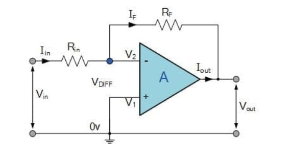
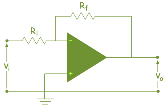
The input signal vi is applied to the inverting input terminal through resistor R1 and non-inverting input terminal is grounded. The feedback from the output of the inverting terminal is provided through the feedback resistor Rf.
Since the input is applied to the inverting terminal vo and vi are opposite in polarity and hence the feedback is negative. Since the non-inverting input terminal is grounded v2=0. Due to virtual short at the input of op-amp the inverting and non-inverting input terminals are at the same potential.
Therefore, v1 = v2 = 0.
Due to high input impedance of Op-amp the current flowing into its inverting input terminal is zero. Therefore, the same current flows through R1 and Rf .
i 1 = i f
But i1 = vi – v1 / R1 = vi/R1
i f = v1 – vo / Rf = -vo/Rf
vi/R1 = - vo/Rf
Af = vo/vi = -Rf/R1
Af is the closed loop voltage gain or voltage gain with negative feedback.
2. Explain non- inverting amplifier?
Non- Inverting amplifier is one in which the output is in phase with respect to input that is if you apply a positive voltage, output will be positive. The output is an non -inverted amplified version of input.
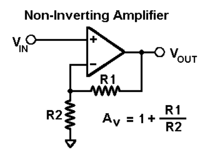
Assuming the op-amp is ideal and applying the concept of virtual short, the voltage at the inverting terminal is equal to non- inverting terminal.
Applying KCL at inverting node we get
Vi -Vo/ R2 + Vo – 0 / R1 = 0
By rearranging the terms, we will get
Voltage gain Av = Vo/ Vi = (1+ Rf/Ri)
Gain of non- inverting amplifier Av= (1+ Rf/Ri).
3.In an op-amp inverting amplifier R1 = 1K Ω and Rf = 100KΩ. The DC supply voltage of the op-amp is ± 15V. Calculate the output voltage if input voltage is 1V.
R1 = 1KΩ Rf = 100KΩ
V+ = 15V and V-=-15V. vi = 1V
Af = -Rf/R1 = -100K/1K = -100
Af = vo/vi
Vo = Af vi
= -100 x 1V = -100V
The output voltage cannot exceed the DC power supply voltage . Since vo is negative and large it is limited to V-
Vo ≈ V- = -15V
4.Explain voltage follower?
Voltage follower

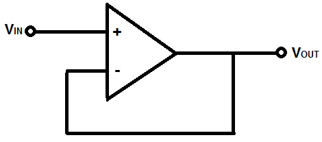
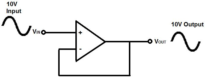
A voltage follower (also called a unity-gain amplifier, a buffer amplifier, and an isolation amplifier) is a op-amp circuit which has a voltage gain of 1.
This means that the op amp does not provide any amplification to the signal. The reason it is called a voltage follower is because the output voltage directly follows the input voltage, meaning the output voltage is the same as the input voltage. Thus, for example, if 10V goes into the op amp as input, 10V comes out as output. A voltage follower acts as a buffer, providing no amplification or attenuation to the signal.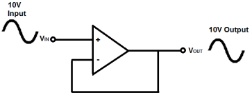
5. Explain summing amplifier?
The summing Amplifier is one variation of inverting amplifier. In inverting amplifier there is only one voltage signal applied to the inverting input as shown below,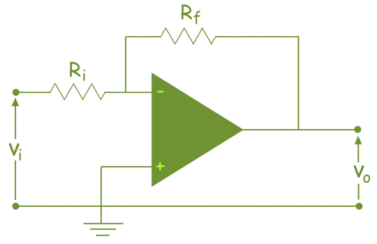
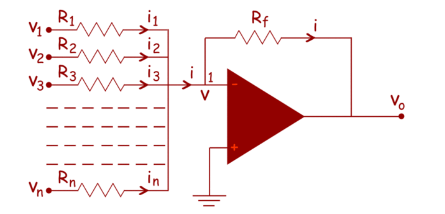
This simple inverting amplifier can easily be modified to summing amplifier, if we connect several input terminals in parallel to the existing input terminals as shown below.
Here, n numbers of input terminal are connected in parallel. Here, in the circuit, the non-inverting terminal of the op amp is grounded, hence potential at that terminal is zero.
As the op amp is considered as ideal op-amp, the potential of the inverting terminal is also zero.
So, the electric potential at node 1, is also zero. From the circuit, it is also clear that the current i is the sum of currents of input terminals.
Therefore,
i = i1 + i2 + i3 +………………………………….+in
i = v1 -0 /R1 + v2 -0 /R2 + v3-0 /R3 +………………+ vn-0/Rn
i = v1/R1 + v2 /R2 + v3 /R3 +……………………………….+ vn/Rn ------(i)
Now, in the case of ideal op amp the current at the inverting and non-inverting terminal are zero. So, as per Kirchhoff’s, the entire input current passes through the feedback path of resistance Rf. That means,
i= 0-vo/Rf = -vo /Rf ---------------------------------(ii)
From, equation (i) and (ii), we get,
v1/R1 + v2/R2 + v3/R3 +……………………..+ vn/Rn = -vo/Rf
vo = -(Rf/R1 v1 + Rf/R2 V2 + Rf/R3 v3 +……………………+Rf/Rn vn )
This indicates that output voltage v0 is weighted sum of numbers of input voltages.
6. Explain differential amplifier?
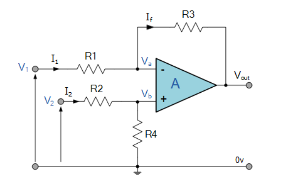
The differential amplifier amplifies the difference between two voltages making this type of operational amplifier circuit a Subtractor This type of operational amplifier circuit is commonly known as a Differential Amplifier.
By connecting each input in turn to 0v ground we can use superposition to solve for the output voltage Vout. Then the transfer function for a Differential Amplifier circuit is given as:
I1 = V1-Va/R1 ; I2 = V2-Vb/R2 ; If = Va –(Vout)/R3
Summing Point Va =Vb
Vb = V2(R4/R2+R4)
If V2 =0 then Vout = -V1 (R3/R1)
If V1=0 then Vout = V2(R4/R2+R4)(R1+R3/R1)
Vout = -Vout (a) + Vout(b)
Vout = -V1(R3/R1) + V2(R4/R2+R4)(R1+R3/R1)
When resistors, R1 = R2 and R3 = R4 the above transfer function for the differential amplifier can be simplified to the following expression:
Vout = (V2 -V1)
The output is the difference between the two inputs hence, the op-amp can be used as subtractor.
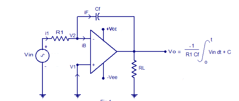
7. Explain practical integrator?
Equation for the instantaneous output voltage of the opamp integrator can be derived as follows.
Applying Kirchoff’s current (KCL) at node V2 we get
i1= iF + iB
Since the input resistance of an opamp is very high (in the range of Mega ohms) iB will be very small at it can be neglected.
Therefore i1 = iF
The relation between the current through a capacitor and voltage across it is
iC = C dv/dt.
Therefore iF= Cf X d (V2 – Vo ) / dt
Also, i1 = (Vin – V2) / R1.
Therefore the equation
i1 = iF
can be rewritten as
(Vin – V2) / R1 = Cf X d(V2 – Vo) / dt……….(1)
Since the non-inverting input is connected to ground, V1 can be taken as 0. Since the open loop gain of the present circuit is near infinity V2 can be assumed to be zero.
So, the equation (1) becomes;
Vin / R1 = Cf X d (-Vo) / dt
Integrating both sides of the above equation with respect to time, we get
 =
=  d(-Vo)/dt = Cf (-Vo) + Vo @ t =0
Rearranging the equation we get
Vo = -1/ (R1Cf) x  + C ----------------------------(2)
C is the integration constant and it has a proportional relationship with the output voltage at time t=0.
From eq(2) it is clear that the output voltage has an inverse relation with the R1 Cf (time constant ) and directly proportional relation with the negative integral of the input voltage.
8. Explain instrumentation amplifier?
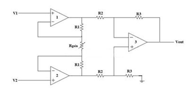
The Instrumentation amplifiers consist of three op-amps. In this circuit, a non-inverting amplifier is connected to each input of the differential amplifier.
This instrumentation amplifier provides high input impedance for exact measurement of input data from transducers. The circuit diagram of an instrumentation amplifier is as shown in the figure below.
The op-amps 1 & 2 are non-inverting amplifiers and together form an input stage of the instrumentation amplifier. The op-amp 3 is a difference amplifier that forms the output stage of the instrumentation amplifier.
Working
The output stage of the instrumentation amplifier is a difference amplifier, whose output Vout is the amplified difference of the input signals applied to its input terminals.
If the outputs of op-amp 1 and op-amp 2 are Vo1 and Vo2 respectively, then the output of the difference amplifier is given by,
Vout = (R3/R2)(Vo1-Vo2)
The expressions for Vo1 and Vo2 can be found in terms of the input voltages and resistances.
Consider the input stage of the instrumentation amplifier as shown in the figure below.
The potential at node A is the input voltage V1. Hence the potential at node B is also V1, from the virtual short concept. Thus, the potential at node G is also V1.
The potential at node D is the input voltage V2. Hence the potential at node C is also V2, from the virtual short. Thus, the potential at node H is also V2.
Ideally the current to the input stage op-amps is zero. Therefore, the current I through the resistors R1, Rgain and R1 remains the same.
Applying Ohm’s law between the nodes E and F,
I = (Vo1-Vo2)/(R1+Rgain+R1) ——————— 1
I = (Vo1-Vo2)/(2R1+Rgain)
Since no current is flowing to the input of the op-amps 1 & 2, the current I between the nodes G and H can be given as,
I = (VG-VH)/Rgain = (V1-V2)/Rgain ————————- 2
Equating equations 1 and 2,
(Vo1-Vo2)/(2R1+Rgain) = (V1-V2)/Rgain
(Vo1-Vo2) = (2R1+Rgain)(V1-V2)/Rgain —————— 3
The output of the difference amplifier is given as,
Vout = (R3/R2) (Vo1-Vo2)
Therefore, (Vo1 – Vo2) = (R2/R3)Vout
Substituting (Vo1 – Vo2) value in the equation 3, we get
(R2/R3)Vout = (2R1+Rgain)(V1-V2)/Rgain
i.e. Vout = (R3/R2){(2R1+Rgain)/Rgain}(V1-V2)
The above equation gives the output voltage of an instrumentation amplifier. The overall gain of the amplifier is given by the term (R3/R2){(2R1+Rgain)/Rgain}.
9. Explain comparator?
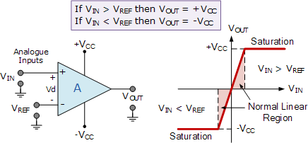
With reference to the op-amp comparator circuit above, lets first assume that VIN is less than the DC voltage level at VREF, ( VIN < VREF ).
As the non-inverting (positive) input of the comparator is less than the inverting (negative) input, the output will be LOW and at the negative supply voltage, -Vcc resulting in a negative saturation of the output.
If we now increase the input voltage, VIN so that its value is greater than the reference voltage VREF on the inverting input, the output voltage rapidly switches HIGH towards the positive supply voltage, +Vcc resulting in a positive saturation of the output.
If we reduce again the input voltage VIN, so that it is slightly less than the reference voltage, the op-amp’s output switches back to its negative saturation voltage acting as a threshold detector.
The op-amp voltage comparator is a device whose output is dependant on the value of the input voltage, VIN with respect to some DC voltage level as the output is HIGH when the voltage on the non-inverting input is greater than the voltage on the inverting input, and LOW when the non-inverting input is less than the inverting input voltage.
This condition is true regardless of whether the input signal is connected to the inverting or the non-inverting input of the comparator.
The value of the output voltage is completely dependent on the op-amps power supply voltage.
However practically, and for obvious reasons it is limited by the op-amps supply rails giving VOUT = +Vcc or VOUT = -Vcc.
The basic op-amp comparator produces a positive or negative voltage output by comparing its input voltage against some preset DC reference voltage. Generally, a resistive voltage divider is used to set the input reference voltage of a comparator, but a battery source, Zener diode or potentiometer for a variable reference voltage can all be used as shown.
10. Explain Schmitt trigger ?
A Schmitt trigger makes use of positive feedback – it takes a sample of the output and feeds it back into the input so as to ‘reinforce’, so to speak, the output – which is the exact opposite to negative feedback, which tries to nullify any changes to the output.
This reinforcing property is useful – it makes the comparator decide the state of the output it wants, and makes it stay there, even within what would normally be the dead zone.
Consider this simple circuit:
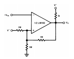
INVERTING COMPARATOR WITH HYSTERESIS
Assume the input voltage is lower than the reference voltage at the non-inverting pin and the output is therefore high.
V* is the reference input voltage which creates a fixed bias at the non-inverting input. Since the output is high through the pullup resistor, this creates a current path through the feedback resistor, slightly increasing the reference voltage.
When the input goes above the reference voltage, the output goes low. There is a feedback resistor, the reference voltage drops slightly below the nominal value because the feedback and the lower reference resistor are now in parallel with respect to ground (since a low output shorts that terminal of the resistor to ground).
Since the reference voltage is lowered, there is no chance of a small change in input causing multiple transitions – in other words, there is no longer a dead zone.
To cause the output to go high, the input must now cross the new lower threshold. Once crossed, the output goes high and the circuit is ‘reset’ to the initial configuration.
The input has to cross the threshold just once resulting in a single clean transition. The circuit now has two effective thresholds or states – it is bi-stable.
This can be summarised in the form of a graph:
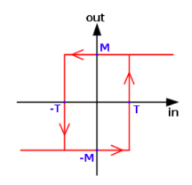
HYSTERESIS CURVE
This can be understood in the usual sense – the x axis is the input and y axis is the output. Tracing a line from x to y, we find that once the lower threshold has been crossed, the hysteresis goes high and vice versa.
The operation of the non-inverting comparator is similar – the output again changes the configuration of a resistor network to change the threshold to prevent unwanted oscillations or noise.
Applications of Schmitt Triggers
Schmitt triggers find a wide range of uses mostly as logic inputs. Again, it’s not a nice thing to have a single logic threshold, in case of noisy or slow signals multiple output transitions may result.
11. Explain square wave generator?
Square wave generator
The square wave generator is based on a uA741 opamp (IC1). Resistor R1 and capacitor C1 determines the frequency of the square wave. Resistor R2 and R3 forms a voltage divider setup which feedbacks a fixed fraction of the output to the non-inverting input of the IC.
If the values of R2 and R3 are made equal, then the frequency of the square wave can be expressed using the following equation
F = 1/(2.1976 R1C1)
12. Explain triangular wave generator ?
The op-amp IC used in this stage is also uA741 (IC2). Resistor R5 in conjunction with R4 sets the gain of the integrator and resistor R5 in conjunction with C2 sets the bandwidth. The square wave signal is applied to the inverting input of the op-amp through the input resistor R4. The op-amp integrator part of the circuit is shown in the figure below.
After this initial “kick” the capacitor starts charging and it creates an opposition to the input current flowing through the input resistor R4. The negative feedback compels the op-amp to produce a voltage at its out so that it maintains the virtual ground at the inverting input.
Since the capacitor is charging its impedance Xc keeps increasing and the gain Xc2/R4 also keeps increasing. This results in a ramp at the output of the op-amp that increases in a rate proportional to the RC time constant (T=R4C2) and this ramp increases in amplitude until the capacitor is fully charged.
When the input to the integrator (square wave) falls to the negative peak the capacitor quickly discharges through the input resistor R4 and starts charging in the opposite polarity.
Now the conditions are reversed, and the output of the op-amp will be a ramp that is going to the negative side at a rate proportional to the R4R2 time constant. This cycle is repeated, and the result will be a triangular waveform at the output of the op-amp integrator.