Unit 6
Converters and PLL
A voltage to current converter or V to I converter, is an electronic circuit that takes current as the input and produces voltage as the output.
An op-amp based voltage to current converter produces an output current when a voltage is applied to its non-inverting terminal. The circuit diagram of an op-amp based voltage to current converter is shown in the following figure.
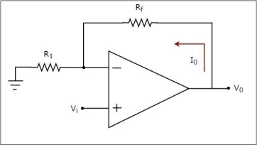
In the circuit shown above, an input voltage Vi is applied at the non-inverting input terminal of the op-amp.
According to the virtual short concept, the voltage at the inverting input terminal of an op-amp will be equal to the voltage at its non-inverting input terminal .
So, the voltage at the inverting input terminal of the op-amp will be Vi.
The nodal equation at the inverting input terminal's node is −
ViR1−I0=0
=>I0=VtR1
Thus, the output current I0 of a voltage to current converter is the ratio of its input voltage Vi and resistance R1.
We can re-write the above equation as −
I0/Vi=1/R1
The above equation represents the ratio of the output current I0 and the input voltage Vi & it is equal to the reciprocal of resistance R1 The ratio of the output current I0and the input voltage Vi is called as Transconductance.
2. Explain current to voltage converter?
A current to voltage converter or I to V converter is an electronic circuit that takes current as the input and produces voltage as the output.
An op-amp based current to voltage converter produces an output voltage when current is applied to its inverting terminal. The circuit diagram of an op-amp based current to voltage converter is shown in the following figure.
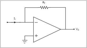
In the circuit shown above, the non-inverting input terminal of the op-amp is connected to ground. That means zero volts is applied at its non-inverting input terminal.
According to the virtual short concept, the voltage at the inverting input terminal of an op-amp will be equal to the voltage at its non-inverting input terminal. So, the voltage at the inverting input terminal of the op-amp will be zero volts.
The nodal equation at the inverting terminal's node is −
−Ii+0−V0/Rf=0
−Ii=V0/Rf
V0=−Rf.Ii
Thus, the output voltage, V0 of current to voltage converter is the (negative) product of the feedback resistance, Rf and the input current, It. Observe that the output voltage, V0 is having a negative sign, which indicates that there exists a 1800 phase difference between the input current and output voltage.
We can re-write the above equation as −
V0/Ii=−Rf
The above equation represents the ratio of the output voltage V0 and the input current Ii, and it is equal to the negative of feedback resistance, Rf. The ratio of output voltage V0 and input current Ii is called as Transresistance.
3. Explain weighted resistor DAC ?
A weighted resistor DAC produces an analog output, which is almost equal to the digital (binary) input by using binary weighted resistors in the inverting adder circuit. In short, a binary weighted resistor DAC is called as weighted resistor DAC.
The circuit diagram of a 3-bit binary weighted resistor DAC is shown in the following figure −
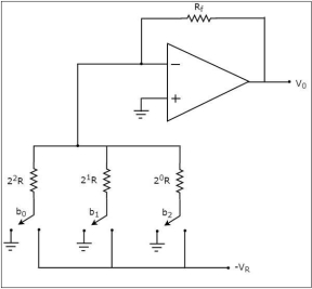
The bits of a binary number can have only one of the two values. i.e., either 0 or 1. Let the 3-bit binary input isb2b1b0. Here, the bits b2 and b0 denote the Most Significant Bit (MSB) and Least Significant Bit (LSB) respectively.
The digital switches shown in the above figure will be connected to ground, when the corresponding input bits are equal to ‘0’
Similarly, the digital switches shown in the above figure will be connected to the negative reference voltage, −VR when the corresponding input bits are equal to ‘1’.
In the above circuit, the non-inverting input terminal of an op-amp is connected to ground. That means zero volts is applied at the non-inverting input terminal of op-amp.
According to the virtual short concept, the voltage at the inverting input terminal of opamp is same as that of the voltage present at its non-inverting input terminal. So, the voltage at the inverting input terminal’s node will be zero volts.
The nodal equation at the inverting input terminal’s node is:
(0 + VR b2) / 2 0 R + 0 + VR b1 / 2 1 R + 0 + VR b0 / 2 2 R + 0 -V0 /Rf =0
Vo /Rf = VR b2 / 2 0 R + VR b1 / 2 1R + VR b0 / 2 2 R
Vo = VR .Rf/ R { b2 / 2 0 + b1 / 2 1 + b0 / 2 2 }
Substituting R = 2Rf in the above equation
Vo = VR . Rf / 2 Rf { b2 / 2 0 + b1 / 2 1 + b0 / 2 2 }
Vo = VR / 2 { b2 / 2 0 + b1 / 2 1 + b0 / 2 2 }
The above equation represents the output voltage equation of a 3-bit binary weighted resistor DAC. Since the number of bits are three in the binary (digital) input, we will get seven possible values of output voltage by varying the binary input from 000 to 111 for a fixed reference voltage, VR.
We can write the generalized output voltage equation of an N-bit binary weighted resistor DAC as shown below based on the output voltage equation of a 3-bit binary weighted resistor DAC.
=>V0=VR/2{bN−1/20+bN−2/21+....+b0/2N−1}
The disadvantages of a binary weighted resistor DAC are as follows −
4. Explain R-2R ladder DAC
The R-2R Ladder DAC overcomes the disadvantages of a binary weighted resistor DAC. As the name suggests, R-2R Ladder DAC produces an analog output, which is almost equal to the digital (binary) input by using a R-2R ladder network in the inverting adder circuit.
Thecircuit diagramof a 3-bit R-2R Ladder DAC is shown in the following figure
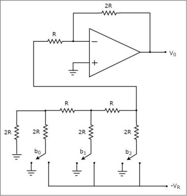
Let the 3-bit binary input is b2b1b0. Here, the bits b2 and b0 denote the Most Significant Bit (MSB) and Least Significant Bit (LSB) respectively.
The digital switches shown in the above figure will be connected to ground, when the corresponding input bits are equal to ‘0’. Similarly, the digital switches shown in above figure will be connected to the negative reference voltage, −VR when the corresponding input bits are equal to ‘1’.
It is difficult to get the generalized output voltage equation of a R-2R Ladder DAC. But, we can find the analog output voltage values of R-2R Ladder DAC for individual binary input combinations easily.
The advantages of a R-2R Ladder DAC are as follows −
5. Explain SAR?
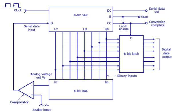
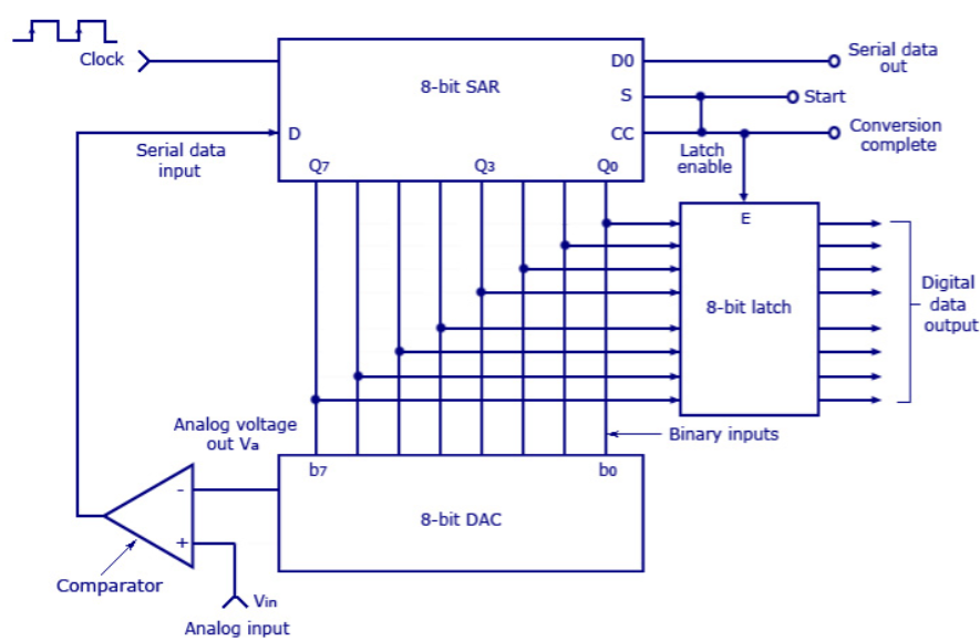
If comparator output is HIGH, D/A output will be less than Vin and the MSB will be set to the next position (Q7 to Q6) by the SAR.
6. Explain flash DAC?
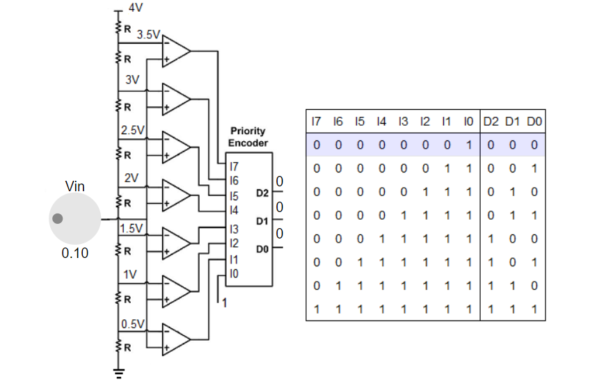
Flash ADC
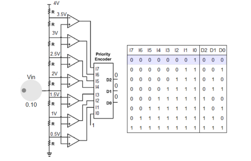
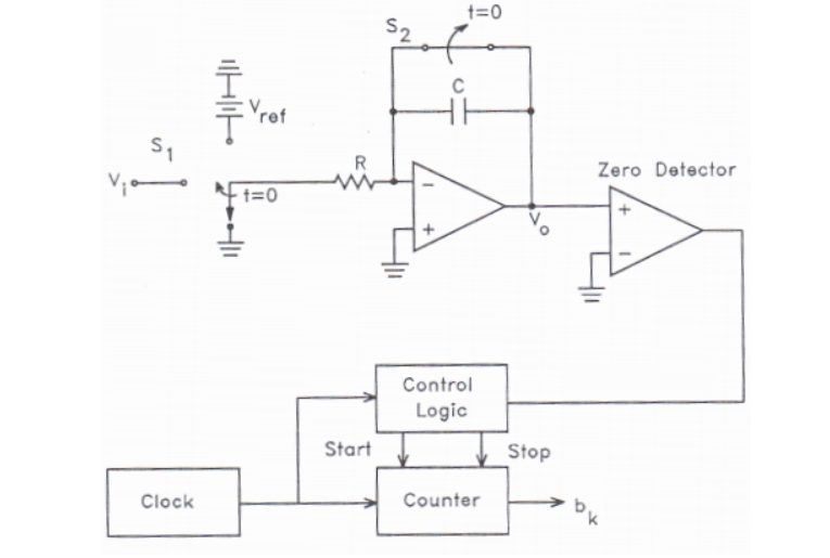
7. Explain Dual slope ADC
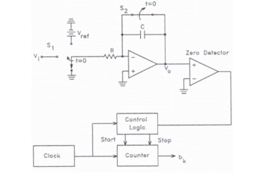
Working:
8. Explain characteristics?
Common mode input range:
The common mode input range can therefore be defined as the range of common mode voltage levels where the ADC produces acceptable output codes.
The two criteria’s shown are where the standard deviation of N conversions is kept within a known boundary whereas the other boundary is how many output codes that can be lost due to the offset in the signal, which will give a lower and an upper bound on what the common mode input should lay between.
Gain:
The ADCs produce the same number of digital codes with the execption that they are spread out over different input ranges, while keeping the location of the mid code centered around Vin,diff = 0.
The gain can therefore be expressed as the range between all zero code and the maximum code, the characteristics of the ADC or the width of an output code, defined as

where N is the resolution of the ADC in number of bits and VFS is the input range of the ADC.
Quantization noise
In an ideal ADC, the only error at the output is due to the quantization of the input values due to the fact that the ADC has a finite resolution of N bits . The quantization error can be described as
e(t) = t, where −q 2 < t < q 2 ,
q is the width of the code
9. Explain the block diagram of ADC?
ADC stands for analog to digital converter. It is an electronic device used for converting an analog signal into a digital signal.
The analog input signal of ADC is continuous time & continuous amplitude signal. The output of ADC is a discrete time and discrete amplitude digital signal.
In the real world, every real quantity such as voice, temperature, weight etc exists in the analog state. And it cannot be processed by any digital device such as a computer or a cell phone.
These analog quantities are converted into digital form so that a digital device can process it. This conversion is done using analog to digital converter.
The analog signal is first applied to the ‘sample‘ block where it is sampled at a specific sampling frequency. The sample amplitude value is maintained and held in the ‘hold‘ block. It is an analog value.
The hold sample is quantized into discrete value by the ‘quantize‘ block. At last, the ‘encoder‘ converts the discrete amplitude into a binary number.
Analog To Digital Conversion StepsThe conversion from analog signal to a digital signal in an analog to digital converter is explained below using the block diagram given above.
SampleThe sample block function is to sample the input analog signal at a specific time interval. The samples are taken in continuous amplitude & possess real value but they are discrete with respect to time.
The sampling frequency plays important role in the conversion. So, it is maintained at a specific rate. The sampling rate is set according to the requirement of the system.
HoldThe second block used in ADC is the ‘Hold’ block. It has no function. It only holds the sample amplitude until the next sample is taken. The hold value remains unchanged till the next sample.
QuantizeThis block is used for quantization. It converts the analog or continuous amplitude into discrete amplitude.
The on hold continuous amplitude value in hold block goes through ‘quantize’ block & becomes discrete in amplitude. The signal is now in digital form as it has discrete time & discrete amplitude.
EncoderThe encoder block converts the digital signal into binary form i.e. into bits.
10. Explain ADC circuits?
In electronics, an Analog to Digital Converter (ADC) is a device for converting an analog signal (current, voltage etc.) to a digital code, usually binary.
In the real world, most of the signals sensed and processed by humans are analog signals.
Analog-to-Digital conversion is the primary means by which analog signal are converted into digital data that can be processed by computers for various purposes as shown in figure.
Audio Signal Processing
There are many types of ADC for different applications.
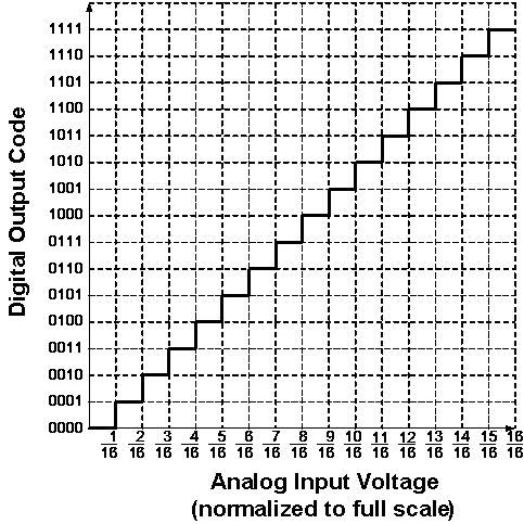
The most inexpensive type of ADC is a Successive-Approximation ADC. Figure shows the transfer curve of a 4-bit ADC.
Inside a Successive-Approximation ADC, a series of digital codes, each corresponds to a fix analog level, are generated successively by an internal counter to compare with the analog signal under conversion.
The generation is stopped when the analog level becomes just larger than the analog signal. The digital code corresponds to the analog level is the desired digital representation of the analog signal.
Ideal Transfer Curve of a 4-bit ADC
The performance of ADCs and DACs mainly depends on their Resolution and Speed.
The Resolution of a converter is expressed in the number of Bit. For an ADC, the Resolution states the number of intervals or levels which can be divided from a certain analog input range. An n-bit ADC has the resolution of 1 / 2n.
For example, the Resolution of a 16-bit ADC is 1 / 65536, since 216 = 65536. If the measuring voltage range is 10 V, then this input range can be resolved into 10 V / 65536 = 0.153 mV precision.
The Speed of a converter is expressed by the Sampling Frequency. It is the number of times that the converter samples the analog signal, its unit is Hertz (Hz).
11. What are the specifications of ADC?
Offset error
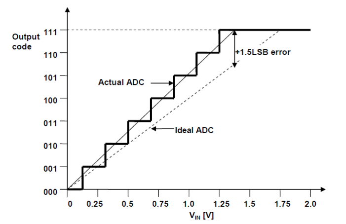
Analog-to-Digital Converter (ADC) offset error is defined as the deviation of the actual ADC’s transfer function from the perfect ADC’s transfer function at the point of zero to the transition measured in the Least Significant Bit (LSB).
When the transition from output value 0 to 1 does not occur at an input value of 0.5 LSB, then we say that there is an offset error.
With positive offset errors, the output value is larger than 0 when the input voltage is less than 0.5 LSB from below.
With negative offset errors, the input value is larger than 0.5 LSB when the first output value transition occurs.
Gain Error
Analog-to-Digital Converter (ADC) gain error is defined as the deviation of the last step’s midpoint of the actual ADC from the last step’s midpoint of the ideal ADC, compensating for offset error.
After compensating for offset errors, applying an input voltage of 0 always results in an output value of 0.
However, gain errors cause the actual transfer function slope to deviate from the ideal slope.
This gain error can be measured and compensated for by scaling the output values. An example of a 3-bit ADC transfer function with gain errors is shown below:

Absolute error
Analog-to-Digital Converter (ADC) absolute error (absolute accuracy) is the total uncompensated error and includes quantization error , offset error , gain error , and non-linearity.
It is the amount of deviation from the ideal ADC transfer function without compensating for gain or offset errors.
The absolute error is also called the total unadjusted error. This error specification gives the designer details of the worst-case ADC performance without any form of error compensation.
Monotocity
An Analog-to-Digital Converter (ADC) is monotonic if, for increasing analog voltage input, the digital output code increases and vice versa. Monotonic behaviour does not guarantee that there will be no missing codes.
Monotonic behaviour is an especially important characteristic for ADCs used in feedback control loops since non-monotonic response can cause oscillations in the system. Monotonicity is a critical specification with automatic control applications.
12. Explain PLL block diagram ?
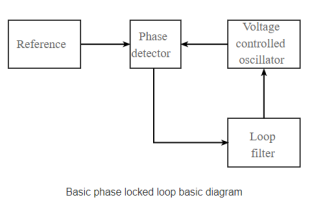
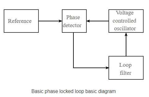
A basic phase locked loop, PLL, consists of three basic elements:
Operation
The diagram for a basic phase locked loop shows the three main element of the PLL: phase detector, voltage- controlled oscillator and the loop filter.
In the basic PLL, reference signal and the signal from the voltage- controlled oscillator are connected to the two input ports of the phase detector.
The output from the phase detector is passed to the loop filter and then filtered signal is applied to the voltage- controlled oscillator.
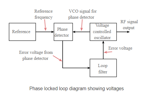
The Voltage Controlled Oscillator, VCO, within the PLL produces a signal which enters the phase detector. The phase of the signals from the VCO and the incoming reference signal are compared and a resulting difference or error voltage is produced. This corresponds to the phase difference between the two signals.
The error signal from the phase detector passes through a low pass filter which governs many of the properties of the loop and removes any high frequency elements on the signal.
Once through the filter the error signal is applied to the control terminal of the VCO as its tuning voltage. The sense of any change in this voltage is such that it tries to reduce the phase difference and hence the frequency between the two signals.
Initially the loop will be out of lock, and the error voltage will pull the frequency of the VCO towards that of the reference, until it cannot reduce the error any further and the loop is locked.
When the PLL, phase locked loop, is in lock a steady state error voltage is produced. By using an amplifier between the phase detector and the VCO, the actual error between the signals can be reduced to very small levels.
However, some voltage must always be present at the control terminal of the VCO as this is what puts onto the correct frequency.
The fact that a steady error voltage is present means that the phase difference between the reference signal and the VCO is not changing. As the phase between these two signals is not changing means that the two signals are on exactly the same frequency.

13. Explain phase detector ?
XOR Phase Detector:

The gain of the phase detector is the ratio between VPD and . When the phase between clkDiv and ClkIn is around /2, VPD is VDD/2, then it increases to VDD.
The gain of the phase detector is the ratio between VPD and . When the phase difference is larger than , the slope sign is negative until 2 .
When locked, the phase difference should be close to /2. The XOR gate output produces a regulator square oscillation VPD when the clk and the signal divin have one quarter of period shift (90 or Π/2).
For other angles output is not regular. Following figure shows CMOS circuit for XOR gate.
14. Explain the applications of PLL?
A PLL may be used to demodulate AM signals as shown in the figure below. The PLL is locked to the carrier frequency of the incoming AM signal. The output of VCO which has the same frequency as the carrier, but unmodulated is fed to the multiplier.
Since VCO output is always 900 before being fed to the multiplier. This makes both the signals applied to the multiplier and the difference signals, the demodulated output is obtained after filtering high frequency components by the LPF.
Since the PLL responds only to the carrier frequencies which are very close to the VCO output, a PLL AM detector exhibits high degree of selectivity and noise immunity which is not possible with conventional peak detector type AM modulators.
FM Demodulation:
If PLL is locked to a FM signal, the VCO tracks the instantaneous frequency of the input signal. The filtered error voltage which controls the VCO and maintains lock with the input signal is the demodulated FM output. The VCO transfer characteristics determine the linearity of thedemodulated output.
Since, VCO used in IC PLL is highly linear, it is possible to realize highly linear FM demodulators.
15. Explain the typical circuits
The PLL is widely used in frequency synthesis to generate spectrally pure signals and, if necessary, to operate as an analog or digital frequency or phase modulator.
Frequency multiplication or division, frequency addition or subtraction may be performed, using a PLL in conjunction with programmable frequency dividers and mixers as shown in Fig.
As a result, the output frequency fo depends on the reference fR and offset fS frequencies, moreover, on the division ratios of frequency dividers. In frequency synthesis, the PLL input is called reference signal and its frequency is denoted by fR.
To optimize the system performance, frequently a multiloop circuit configuration is used.
In frequency synthesis, the dominant noise sources are the VCO, frequency dividers, mixers, and phase detectors.
The main design goals are to minimize the output phase noise, to avoid the generation of spurious output signals, and to minimize the unwanted output FM caused by the periodic output of the phase detector.
These requirements can be satisfied with special PD configurations, such as sample-and-hold phase detector or phase-frequency detector with a charge-pump circuit.
In addition to frequency synthesis, PLLs may be also used as FM or PM modulators.
The corresponding transfer functions for FM and PM are
sΘo(s) = [1 − H(s)]KvVFM(s)
Θo(s) = H(s) N AK VPM(s) (3)
where Kv and N/(AK) are the gains of the FM and PM modulators, respectively.
H(s) and [1 − H(s)] denote the closed-loop transfer and error functions, respectively.
However, since the frequency synthesizer has a frequency divider in the feedback path, the loop gain becomes
K = KgKdKv
