Unit - 4
Peripheral Support in PIC 18FXXXX
Q1) WAP Sample code to blink the LEDs with 1ms delay.
A1)
#include<pic16f877a.h>
Char value = 0;
#define SBIT_PS2 2
Void interrupt timer_isr()
{
If(TMR0IF==1)
{
Value=~value; // complement the value for blinking the LEDs
TMR0 = 101; /*Load the timer Value, (Note: Timervalue is 101 instaed of 100 as the
TImer0 needs two instruction Cycles to start incrementing TMR0 */
TMR0IF=0; // Clear timer interrupt flag
}
}
Void main()
{
TRISD=0x00; //COnfigure PORTD as output to blink the LEDs
OPTION_REG = (1<<SBIT_PS2); // Timer0 with external freq and 32 as prescalar
TMR0=100; // Load the time value for 1ms delay
TMR0IE=1; //Enable timer interrupt bit in PIE1 register
GIE=1; //Enable Global Interrupt
PEIE=1; //Enable the Peripheral Interrupt
While(1)
{
PORTD = value;
}
}
Q2) Delay Calculations for 100ms @20Mhz with Prescalar as 8: $$RegValue = 65536-(Delay * Fosc)/(Prescalar*4)) = 65536-((100ms * 20Mhz)/(8*4)) = 3036 = 0xBDC44
A2)
Steps to configure by using the Timer1 for delay generation:
- Calculate the Timer Count for required delay.
- Set the Pre-scalar bits in T1CON as per the delay calculations.
- With the help of TMR1CS bit Select the Clock Source Internal/External
- Load the timer value into registers TMR1H, TMR1L.
- For Enabling the Timer1 Interrupt set TMRIE bit
- For Enabling the Global and Peripheral interrupts set GIE and PIE bits.
- Start the timer by setting TMR1ON bit.
#include<pic16f877a.h>
Char value = 0;
#define SBIT_PS1 5
#define SBIT_PS0 4
Void interrupt timer_isr()
{
If(TMR1IF==1)
{
Value=~value; // complement the value for blinking the LEDs
TMR1H=0x0B; // Load the time value(0xBDC) for 100ms delay
TMR1L=0xDC;
TMR1IF=0; // Clear timer interrupt flag
}
}
Void main()
{
TRISD=0x00; //COnfigure PORTD as output to blink the LEDs
T1CON = (1<<SBIT_PS1) | (1<<SBIT_PS0); // Timer0 with external freq and 8 as prescalar
TMR1H=0x0B; // Load the time value(0xBDC) for 100ms delay
TMR1L=0xDC;
TMR1IE=1; //Enable timer interrupt bit in PIE1 register
GIE=1; //Enable Global Interrupt
PEIE=1; //Enable the Peripheral Interrupt
TMR1ON = 1; //Start Timer1
While(1)
{
PORTD = value;
}
}
Q3) Write a program to calculate the timer count for the required delay?
A3)
Steps:
- Calculate the Timer Count for the required delay.
- Set the Presaclar bits in OPTION_REG as per the delay calculations.
- Clear the PSAbit for using the prescalar.
- Select the Clock Source Internal/External using TOCS bit.
- Load the timer value into TMRO register.
- Enable the Timer0 Interrupt by setting TMR0IE bit
- Enable the Global and Peripheral interrupts by setting GIE and PIE bits
#include<pic16f877a.h>
Char value = 0;
#define SBIT_PS2 2
Void interrupt timer_isr()
{
If(TMR0IF==1)
{
Value=~value; // complement the value for blinking the LEDs
TMR0 = 101; /*Load the timer Value, (Note: Timervalue is 101 instaed of 100 as the
TImer0 needs two instruction Cycles to start incrementing TMR0 */
TMR0IF=0; // Clear timer interrupt flag
}
}
Void main()
{
TRISD=0x00; //COnfigure PORTD as output to blink the LEDs
OPTION_REG = (1<<SBIT_PS2); // Timer0 with external freq and 32 as prescalar
TMR0=100; // Load the time value for 1ms delay
TMR0IE=1; //Enable timer interrupt bit in PIE1 register
GIE=1; //Enable Global Interrupt
PEIE=1; //Enable the Peripheral Interrupt
While(1)
{
PORTD = value;
}
}
Q4) Write a program to calculate the timer 1 count for the required delay?
A4)
Steps:
• Calculate the Timer Count for the required delay.
• Set the Presaclar bits in T1CON as per the delay calculations.
• Select the Clock Source Internal/External using TMR1CS bit.
• Load the timer value into TMR1H, TMR1L register.
• Enable the Timer1 Interrupt by setting TMRIE bit
• Enable the Global and Peripheral interrupts by setting GIE and PIE bits
• Finally start the timer by setting TMR1ON bit
#include<pic16f877a.h>
Char value = 0;
#define SBIT_PS1 5
#define SBIT_PS0 4
Void interrupt timer_isr()
{
If(TMR1IF==1)
{
Value=~value; // complement the value for blinking the LEDs
TMR1H=0x0B; // Load the time value(0xBDC) for 100ms delay
TMR1L=0xDC;
TMR1IF=0; // Clear timer interrupt flag
}
}
Void main()
{
TRISD=0x00; //COnfigure PORTD as output to blink the LEDs
T1CON = (1<<SBIT_PS1) | (1<<SBIT_PS0); // Timer0 with external freq and 8 as prescalar
TMR1H=0x0B; // Load the time value(0xBDC) for 100ms delay
TMR1L=0xDC;
TMR1IE=1; //Enable timer interrupt bit in PIE1 register
GIE=1; //Enable Global Interrupt
PEIE=1; //Enable the Peripheral Interrupt
TMR1ON = 1; //Start Timer1
While(1)
{
PORTD = value;
}
}
Q5) Write a program for timer 2 for the required delay?
A5)
- Calculate the Timer Count for the required delay.
- Set the Prescaler bits in T2CON as per the delay calculations.
- Load the timer value into TMR2 register.
- Enable the Timer2 Interrupt by setting TMR2IE bit
- Enable the Global and Peripheral interrupts by setting GIE and PIE bits
- Finally start the Timer2 by setting TMR2ON bit
#include<pic16f877a.h>
#define SBIT_T2CKPS1 1
Char value = 0;
Int count = 0;
Void interrupt timer_isr()
{
If(TMR2IF==1)
{
TMR2 = 101; /*Load the timer Value, (Note: Timervalue is 101 instead of 100 as the
Timer2 needs two instruction Cycles to start incrementing TMR2 */
TMR2IF=0; // Clear timer interrupt flag
If(count>=2000) //500us * 2000=1000000us=1sec
{
Count=0;
Value=~value; // complement the value for blinking the LEDs
}
Else
{
Count++; // Keep incrementing the count till it reaches 2000 to generate 1sec delay
}
}
}
Void main()
{
TRISD=0x00; //COnfigure PORTD as output to blink the LEDs
T2CON = (1<<SBIT_T2CKPS1); // Timer2 with external freq and 16 as prescalar
TMR2=100; // Load the timer value for 500us delay
TMR2IE=1; //Enable timer interrupt bit in PIE1 register
GIE=1; //Enable Global Interrupt
PEIE=1; //Enable the Peripheral Interrupt
TMR2ON = 1;
While(1)
{
PORTD = value;
}
}
Q6) WAP for LED Toggling using PIC18F4550 External Interrupt?
A6)
#include "osc.h"
#include <p18f4550.h>
#define LED LATC
Void External_Interrupt_Init();
Void MSdelay(unsigned int);
Void main()
{
OSCCON=0x72; /* Set internal oscillator to 8MHz*/
TRISC0=0; /* Make PORTC.0 as output*/
LED=0;
External_Interrupt_Init(); /* Initialize External Interrupt*/
While(1);
}
Void External_Interrupt_Init()
{
TRISBbits.TRISB0=1; /* Make INT0 pin as an input pin*/
/* Also make PBADEN off in Configuration file or
Clear ADON in ADCON0 so as to set analog pin as digital*/
INTCON2=0x00; /* Set Interrupt on falling Edge*/
INTCONbits.INT0IF=0; /* Clear INT0IF flag*/
INTCONbits.INT0IE=1; /* Enable INT0 external interrupt*/
INTCONbits.GIE=1; /* Enable Global Interrupt*/
}
Void interrupt ISR()
{
LED = ~(LED); /* Toggle LED on interrupt*/
MSdelay(200);
INTCONbits.INT0IF=0;
}
Void MSdelay(unsigned int val)
{
Unsigned int i,j;
For (i=0; i<val; i++)
For (j=0; j<165; j++); /* Delay count for 1ms for 8MHz freq. */
}
Q7) WAP for Setup Timer1 for Timer or Counter Mode?
A7)
[ For Timer Mode]
// -- [[ Configure Timer1 To Operate In Timer Mode]] --
// Clear The Timer1 Register. To start counting from 0
TMR1 = 0;
// Choose the local clock source (timer mode)
TMR1CS = 0;
// Choose the desired prescaler ratio (1:1)
T1CKPS0 = 0;
T1CKPS1 = 0;
[ For Counter Mode ]
//--[ Configure The Timer1 Module To Operate In Counter Mode ]--
TMR1 = 0;
// Choose the desired prescaler ratio (1:1)
T1CKPS0 = 0;
T1CKPS1 = 0;
// Choose the extrenal clock source (counter mode)
TMR1CS = 1;
T1OSCEN = 1;
// Enable Synchronization For Counter Mode
T1SYNC = 0;
//--[ Configure The Timer1 Module To Operate In Counter Mode ]--
TMR1 = 0;
// Choose the desired prescaler ratio (1:1)
T1CKPS0 = 0;
T1CKPS1 = 0;
// Choose the external clock source (counter mode)
Q8) Write the ISR Handler For CCP-Compare Interrupt?
A8)
Void interrupt ISR()
{
If (CCP1IF)
{
// Do Some Stuff...
}
}
Program:
#include <xc.h>
#include "config.h"
#include <stdint.h>
Uint8_t X=0; // Counter For Compare Match Events
Void main(void)
{
//--[ Configure The IO Ports ]--
// Set The Output Pin For The LED
TRISC4=0;
RC4=0; // Initially OFF
//--[ Configure The Timer1 Module To Operate In Timer Mode ]--
TMR1 = 0;
T1CKPS0 = 0;
T1CKPS1 = 0;
TMR1CS = 0;
TMR1ON = 1;
//--[ Configure The CCP1 Module To Operate in Compare Mode ]--
// Preload The CCPR1 Register
CCPR1 = 50000;
// CCP in Compare Mode, CCPx Pin Is Unchanged & Trigger Special Event
CCP1M0 = 1;
CCP1M1 = 1;
CCP1M2 = 0;
CCP1M3 = 1;
// Enable CCP1 Interrupt
CCP1IE = 1;
PEIE = 1;
GIE = 1;
// Create The Main Loop Of The System
While (1)
{
// Stay Idle, everything is taken care of in the ISR
}
Return;
}
// Write The ISR Handler
Void interrupt ISR()
{
If ( CCP1IF )
{
X++;
If (X==10)
{
// Toggle The LED
RC4 = ~RC4;
X = 0;
}
// Clear The Interrupt Flag Bit
CCP1IF = 0;
}
}
Q9) Write a program for PR2 register Configure T2CON register and set the TMR2 register to 0. Also, start the Timer2.
A9)
Steps:
- Load the PR2 value which will decide the period of the pulse.
- Set the duty cycle by loading a value in the CCPR1L: CCP1CON<5: 4>
- Configure the CCP1CON register for setting a PWM mode.
- Initialize the pin CCP1as an output pin which will give PWM output.
- Configure the T2CON register and enable TMR2 using T2CON
#include "osc_config.h"
#include <pic18f4550.h>
Void main()
{
OSCCON = 0x72; /* Set internal clock to 8MHz */
TRISC2 = 0; /* Set CCP1 pin as output for PWM out */
PR2 = 199; /* Load period value */
CCPR1L = 40; /* load duty cycle value */
T2CON = 0; /* No pre-scalar, timer2 is off */
CCP1CON = 0x0C; /* Set PWM mode and no decimal for PWM */
TMR2 = 0; /* Clear Timer2 initially */
TMR2ON = 1; /* Timer ON for start counting*/
While(1);
}
Q10) WAP for interfacing of 8051 with DC motor circuit?
A10)
We use 20MHz clock and the o/p frequency is 2KHz;
Whereas PWM period = 1/frequency (that will be 1/2000 = .0005)


Program:
Void main()
{
Short duty = 0; //initial value for duty
TRISD = 0xFF; //PORTD as input
TRISC = 0x00; //PORTC as output
TRISB = 0x00; //PORTB as output
PORTB = 0x02; //Run motor in anticlock wise
PWM1_Init(1000); //Initialize PWM1
PWM1_Start(); //start PWM1
PWM1_Set_Duty(duty); //Set current duty for PWM1
While (1) // endless loop
{
If (!RD0_bit && duty<260) //if button on RD0 pressed
{
Delay_ms(40);
Duty = duty + 10; //increment current_duty
PWM1_Set_Duty(duty); //Change the duty cycle
}
If (!RD1_bit && duty >0) //button on RD1 pressed
{
Delay_ms(40);
Duty = duty - 10; //decrement duty
PWM1_Set_Duty(duty);
}
Delay_ms(10); // slow down change pace a little
}
}
Q11) WAP to interfacing of Temperature sensor with microcontroller?
A11)
ORG 00H
MOV P1,#11111111B // initializes P1 as input port
MOV P0,#00000000B // initializes P0 as output port
MOV P3,#00000000B // initializes P3 as output port
MOV DPTR,#LABEL // loads the address of "LABEL" to DPTR
MAIN: MOV R4,#250D // loads register R4 with 250D
CLR P3.7 // makes Cs=0
SETB P3.6 // makes RD high
CLR P3.5 // makes WR low
SETB P3.5 // low to high pulse to WR for starting conversion
WAIT: JB P3.4,WAIT // polls until INTR=0
CLR P3.7 // ensures CS=0
CLR P3.6 // high to low pulse to RD for reading the data from ADC
MOV A,P1 // moves the digital output of ADC to accumulator A
MOV B,#10D // load B with 10D
DIV AB // divides the content of A with that in B
MOV R6,A // moves the quotient to R6
MOV R7,B // moves the remainder to R7
DLOOP:SETB P3.2 // sets P3.2 which activates LED segment 1
MOV A,R6 // moves the quotient to A
ACALL DISPLAY // calls DISPLAY subroutine
MOV P0,A // moves the content of A to P0
ACALL DELAY // calls the DELAY subroutine
CLR A // clears A
MOV A,R7 // moves the remainder to A
CLR P3.2 // deactivates LED segment 1
SETB P3.1 // activates LED segment 2
ACALL DISPLAY
MOV P0,A
ACALL DELAY
CLR A
CLR P3.1 // deactivates LED segment 2
DJNZ R4,DLOOP // repeats the loop "DLOOP" until R4=0
SJMP MAIN // jumps back to the main loop
DELAY: MOV R3,#255D // produces around 0.8mS delay
LABEL1: DJNZ R3,LABEL1
RET
DISPLAY: MOVC A,@A+DPTR // converts A's content to corresponding digit drive pattern
RET
LABEL: DB 3FH // LUT (look up table) starts here
DB 06H
DB 5BH
DB 4FH
DB 66H
DB 6DH
DB 7DH
DB 07H
DB 7FH
DB 6FH
END
Q12) Write and explain the ADCONO control register 0?
A12)
The PIC 18F4321 contains an on‑chip A/D converter (or sometimes called ADC) module with 13 channels (AN0-AN12). An analog input can be selected as an input on one of these 13 channels, and can be converted to a corresponding 10‑bit digital number. Three control registers, namely, ADCON0 through ADCON2, are used to perform the conversion. The ADCON0 register, shown in Figure below, controls the operation of the A/D module. The ADCON0 register can be programmed to select one of 13 channels using bits CHS3 through CHS0 (bits 5 through 2). The conversion can be started by setting the GO/ DONE (bit 1) to 1. Once the conversion is completed, this bit is automatically cleared to 0 by the PIC18F4321. The ADCON1 register, shown in Figure below, configures the functions of the port pins as Analog (A) input or Digital (D) I/O.

Bit 7-6 Unimplemented: Read as ‘0’
Bit 5-2 CHS3:CHS0: Analog Channel Select
Bits 0000 = Channel 0 (AN0)
0001 = Channel 1 (AN1)
0010 = Channel 2 (AN2)
0011 = Channel 3 (AN3)
0100 = Channel 4 (AN4)
0101 = Channel 5 (AN5)
0110 = Channel 6 (AN6)
0111 = Channel 7 (AN7)
1000 = Channel 8 (AN8)
1001 = Channel 9 (AN9)
1010 = Channel 10 (AN10)
1011 = Channel 11 (AN11)
1100 = Channel 12 (AN12)
1101 = Unimplemented
1110 = Unimplemented
1111 = Unimplemented
Bit 1 GO/ DONE: A/D Conversion Status bit
When GO/DONE = 1:
1 = A/D conversion in progress
0 = A/D idle
Bit 0 ADON: A/D On bit
1 = A/D converter module is enabled
0 = A/D converter module is disabled
Q13) Write the steps involved to be followed to perform an A/D conversion?
A13)
The following steps should be followed to perform an A/D conversion:
Configure the A/D module
- Configure analog pins, voltage reference, and digital I/O (ADCON1)
- Select A/D input channel (ADCON0)
- Select A/D acquisition time (ADCON2)
- Select A/D conversion clock (ADCON2) • Turn on A/D module (ADCON0)
Configure A/D interrupt (if desired)
- Clear ADIF bit (bit 6 of PIR1)
- Set ADIE bit
- Set GIE bit (bit 7) and PEIE (bit 6) of INTCON register
- All interrupts including A/D Converter interrupt, branch to address 0x000008 (default) upon power‑on reset. However, the A/D Converter interrupt can be configured as low priority by setting the ADIP bit (bit 6) of the IPRI register to branch to address 0x000018. The instruction, BSF IPR1, ADIP can be used for this purpose.
Wait for the required acquisition time (if required).
Start conversion:
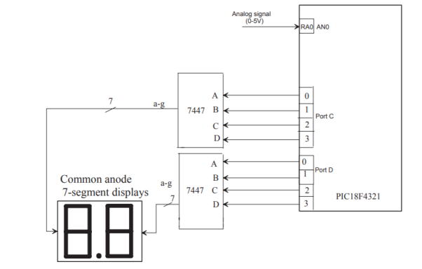
Figure: Interfacing of on-chip ADC
Q14) Explain timer 1 register with every register configuration?
A14)
Timer 1
The timer TMR1 module is 16-bit timer/counter with features such as:
- 16-bit timer/counter with two 8-Bit register TMR1H/TMR1L
- Writeable and Readable
- Software programmable pre-scaler upto 1:8
- Internal or external clock select
- Interrupt on overflow from FFFFh to 00h
- Edge selects for external clock.
Timer 1 Register
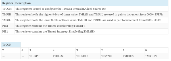
T1CKPS1:T1CKPS0: Timer1 Input Clock Pre-scale Select bits
11 = 1:8 pre-scale value
10 = 1:4 pre-scale value
01 = 1:2 pre-scale value
00 = 1:1 pre-scale value
T1OSCEN: Timer1 Oscillator Enable Control bit
1-Oscillator is enabled
0-Oscillator is shut-off
T1SYNC: Timer1 External Clock Input Synchronization Control bit
1-Do not synchronize external clock input
0-Synchronize external clock input
TMR1CS: Timer1 Clock Source Select bit
1-External clock from pin RC0/T1OSO/T1CKI (on the rising edge)
0-Internal clock (FOSC/4)
TMR1ON: Timer1 On bit
1-Enables Timer1
0-Stops Timer1
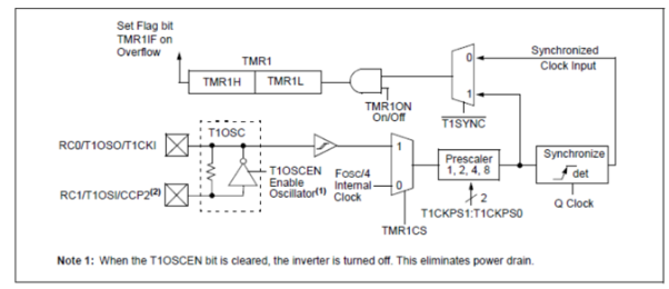
Fig: Timer 1 Block Diagram
Q15) Explain the configuration of external PIC interrupts INTCON?
A15)
INTCON Register
INTCON registers are used to configure the external PIC interrupts.

GIE: Global Interrupt Enable
This bit is set high to enable all interrupts of PIC 18F452
1-Enable all interrupts
0- Disable all interrupts
PEIE: Peripheral Interrupt Enable
This bit is set high to enable all peripheral interrupts of the microcontroller.
1- Enable all peripheral interrupts
0 – Disable all peripheral interrupts.
TOIE – TMR) Overflow Interrupt Enable
This bit is set high to enable External Interrupt 0
1 – Enable TMRO overflow interrupt
0 – Disable TMR0 overflow interrupt
INTE: INT External Interrupt Enable
This bit is set to enable external interrupts
1-Enable the INT external interrupt
0 – Disable the INT external interrupt
RBIE: RB Interrupt enable
This bit is set high to enable the RB port Change interrupt pin.
1 – Enables the RB port change interrupt
0 - Disables the RB port change interrupt
T0IF: TMR0 Overflow Interrupt Flag
1 – TMR0 register has overflowed
0 – TMR0 register has not overflowed
INTF: INT External Interrupt Flag
1 – INT external interrupt occurred
0 – INT external interrupt did not occur.
RBIE – RB port Change Interrupt Flag
1 – At least one of the RB7:RB4 pins changed the state
0 – Disables the RB port change interrupt.
T0IF: TMR0 Overflow Interrupt flag
1- TMR0 register has overflowed.
0 – TMR0 has not overflowed.
INTF: INT External Interrupt flag
1 –The INT external interrupt occurred.
0 – The INT external interrupt has not occurred.
RBIF: RB port change interrupt priority
1 - At least one of the RB7:RB4 pins changed the state
0 – None of the pins have changed the state.
INTCON2 Register:

RBPU: Port B Pull up Enable
1= All port B pull ups are diabled
0=All port b pull ups are enabled by individual port latch values
INTEDG0, INTEDG1, INTEDG2: External Interrupt Edge
These bits are used to select the triggering edge of the corresponding interrupt signal on which the microcontroller is to respond.
1=interrupt on rising edge
0= interrupt on falling edge
Bit 3, Bit 1: Unimplemented
It is always read as 0
TMR0IP: TMR0 overflow priority
1=High Priority
0=Low Priority
RBPIP: RB Port change Interrupt Priority
1=High Priority
0=Low Priority
Q16) Explain PORTB change interrupts in detail?
A16)
This “interrupt on change” is triggered when any of the RB7:RB4 pins, configured as an input, changes level. When this interrupt is used in conjunction with the software programmable weak internal pull-ups, a direct interface to a keypad is possible. This is shown in application note AN552, Implementing Wake-up on Key Stroke. Another way to use the “interrupt on change” feature would be as additional external interrupt sources. This allows PIC16CXXX devices to support multiple external interrupts, in addition to the built-in external interrupt on the INT pin.
The interrupt source(s) cannot simply be directly connected to the PORTB pins, and expect an interrupt to occur the same as on the interrupt (INT) pin. To develop the microcontrollers hardware/software to act as an interrupt by an external signal, we must know the characteristics of the external signal. After we know this, we can determine the best way to structure the program to handle this signal. The characteristics that we need to consider when developing the interrupt include:
1. The rising edge and falling edges.
2. The pulse width of the interrupt trigger (high time / low time).
It is easy to understand the need of knowing about which edge triggers the interrupt service routine for the external interrupt. This allows one to ensure that the interrupt service routine is only entered for the desired edge, with all other edges ignored. Not so clear is the pulse width of the interrupt’s trigger. This characteristic helps determine the amount of additional overhead that the software routine may need.
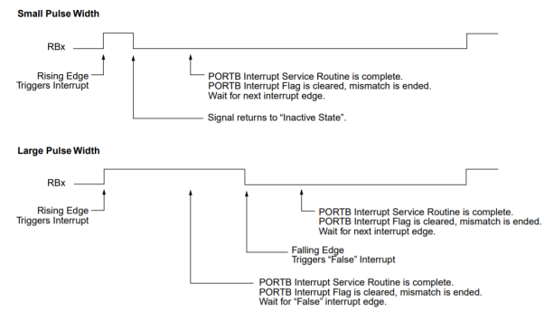
Figure: Interrupt steps for small and wide pulse widths
Figure above shows the two cases for the interrupt signal verses the time to complete the interrupt service routine. The first waveform is when the signal makes the low-to-high-to-low transitions before the interrupt service routine has completed (interrupt flag cleared). When the interrupt flag has been cleared, the interrupt signal has already returned to the inactive level. The next transition of the signal is due to another interrupt request. An interrupt signal with this characteristic will be called a small pulse width signal. The second waveform is when the signal only makes the low-to-high transitions before the interrupt service routine has completed (interrupt flag cleared). The next transition (high-to-low) will return the interrupt signal to the inactive level. This will generate a “false” interrupt, that will need to be cleared. Then the following transition (low-to-high) will be a “true” interrupt. An interrupt signal with this characteristic will be called a wide pulse width signal.
An interrupt pulse with a small pulse width requires less overhead than a wide pulse width. A small pulse width signal must be less than the minimum execution time of the interrupt service routine, while a wide pulse width must be greater then, the maximum time through the interrupt service routine.
Q17) Explain the sensor interfacing using ADC with microcontroller?
A17)
In case of temperature the Celsius and Fahrenheit scale thermometer displays the ambient temperature through LCD display.
This consists of two sections:
- One senses the temperature. The temperature sensor is LM 35.
- The other converts the temperature value into a suitable number in Celsius scale by ADC0804.
The temperature is sensed in Celsius scale and converted into Fahrenheit scale temperature by using Celsius to Fahrenheit conversion formulae.
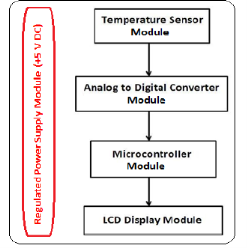
Figure: Process
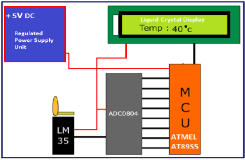
Figure: Circuit Diagram
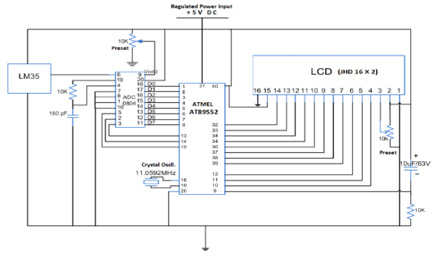
Figure: Interfacing of Temperature sensor with microcontroller
- The temperature sensor used is LM35. The LM 35 IC generates a 10mV variation in its output voltage for every degree Celsius change in temperature. The output of the temperature sensor is analog in nature.
- Hence, there is a need for analog to digital convertor to convert the analog input to its equivalent binary output.
- The ADC 0804 is the analog to digital convertor IC. It is a single channel converter that converts the analog input up to a range of 5V into its equivalent 8-bit binary output.
- The step size is defined by the voltage applied at Vref/2 pin of the ADC IC.