Unit - 6
Serial Port Programming interfacing with 18FXXXX
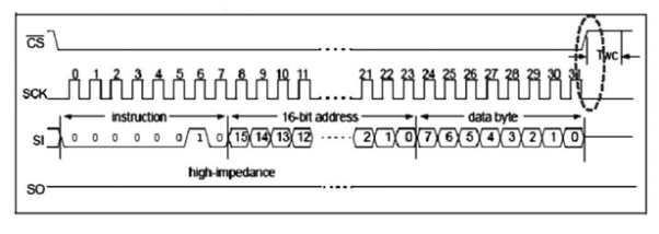
Q1) Write an Embedded C program to interface Serial EEPROM IC 25CXXX with PIC18FXXXX using SPI protocol and write a character and read the same character and display it on to the LED's
A1)
//Program to Write and read from SPI EEPROM 25Cxxx
//Write a character and read it to display the read data on LED
#include <p18f4550.h>
#pragma config FOSC = HS //Oscillator Selection
#pragma config WDT = OFF //Disable Watchdog timer
#pragma config LVP = OFF //Disable Low Voltage Programming
#pragma config PBADEN = OFF //Disable PORTB Analog inputs
/*Declare PORT pin to use as chip select/Slave select*/
#define CS_EEPROM_TRIS TRISAbits.TRISA5
#define CS_EEPROM PORTAbits.RA5
/************ SPI EEPROM Commands *******************/
#define EEPROM_CMD_READ (unsigned)0b00000011
#define EEPROM_CMD_WRITE (unsigned)0b00000010
#define EEPROM_CMD_WRDI (unsigned)0b00000100
#define EEPROM_CMD_WREN (unsigned)0b00000110
#define EEPROM_CMD_RDSR (unsigned)0b00000101
#define EEPROM_CMD_WRSR (unsigned)0b00000001
//Function Prototypes
void msdelay (unsigned int time); //Function to generate delay
void SPIinit(); //Function to Initialize SPI Module
unsigned char SPISend(unsigned char data); //Function to send data to SPI Slave
unsigned char SPIReceive(); //Function to receive data from SPI Slave
//Function to Write the single byte to SPI EEPROM IC
void EEPROMWriteByte(unsigned char Data, unsigned int Address);
//Funcction to read the single byte from SPI EEPROM IC
unsigned char EEPROMReadByte(unsigned int Address);
//Start of Main Program void main(void)
{
unsigned char rx_data;
TRISD = 0x00; //Configuring PORTD as output
PORTD = 0x00; //Initially PORTD made low
SPIinit(); //Initializing SPI module
EEPROMWriteByte(0xAA, 0x0010); //Write Data to SPI EEPROM
msdelay(500);
rx_data = EEPROMReadByte(0x10); //Read Data from SPI EEPROM
PORTD = rx_data; //Verify the data using PORTD
while(1); //Endless loop
} //End of main program
//Function Definitions //Function to generate delay void msdelay (unsigned int time)
{
unsigned int i, j;
for (i = 0; i< time; i++)
for (j = 0; j < 275; j++);/*Calibrated for a 1 ms delay in MPLAB*/
}
//Function to Initialize SPI Module void SPIinit()
{
TRISCbits.TRISC3=0; //SCK = output
TRISCbits.TRISC5=1; //SDI = input
TRISCbits.TRISC4=0; //SDO = output
PORTCbits.RC3=0; //Clearing SDO,SCK initially
PORTCbits.RC4=0;
CS_EEPROM_TRIS=0; //Chip select pin = Output
CS_EEPROM =1; //Initially slave not selected
SSPSTATbits.SMP=1; //1 = Input data sampled at end of data output time
SSPSTATbits.CKE=1; //1 = Transmit occurs on transition from active to idle clock state
SSPCON1=0X02; //SPI Master mode, clock = FOSC/64
SSPCON1bits.SSPEN=1; //Enabling SPI module
}
//Function to send data to SPI Slave
unsigned char SPISend(unsigned char data)
{ //Load SSPBUF with data
SSPBUF=data;
while(!SSPSTATbits.BF); //Check for Buffer full status
}
//Function to receive data from SPI Slave unsigned char SPIReceive()
{
SSPBUF=0x0; //dummy write to receive data while(!SSPSTATbits.BF); //Check for Buffer full status return(SSPBUF); //return the received data
}
//Function to Write the single byte to SPI EEPROM IC
void EEPROMWriteByte(unsigned char Data, unsigned int Address)
{
unsigned char low_address, high_address;
low_address = (unsigned char)(Address & 0x00ff); //Separate out lower address
high_address = (unsigned char)((Address>>8)&0x00ff); //Separate out higher address
//Send the Wrtie Enable Command to SPI EEPROM CS_EEPROM =0;
SPISend(EEPROM_CMD_WREN); CS_EEPROM =1;
//Write the Data to SPI EEPROM
CS_EEPROM =0;
SPISend(EEPROM_CMD_WRITE); //Send Write Command
SPISend(high_address); //Send Higher Address (A15 - A8)
SPISend(low_address); //Send Lower Address (A7 - A0)
SPISend(Data); //Send data to be written
CS_EEPROM =1;
msdelay (100); //Keep Some delay before disabling
//Send the Wrtie Disable Command to SPI EEPROM CS_EEPROM =0;
SPISend(EEPROM_CMD_WRDI); CS_EEPROM =1;
}
//Funcction to read the single byte from SPI EEPROM IC unsigned char EEPROMReadByte(unsigned int Address)
{
unsigned char temp;
unsigned char low_address, high_address;
low_address = (unsigned char)(Address & 0x00ff); //Separate out lower address high_address = (unsigned char)((Address>>8)&0x00ff); //Separate out higher address
CS_EEPROM =0;
SPISend(EEPROM_CMD_READ); //Send Read Command
SPISend(high_address); //Send Higher Address (A15 - A8)
SPISend(low_address); //Send Lower Address (A7 - A0)
temp = SPIReceive(); //Read the data from specified location
CS_EEPROM =1;
return temp; //return the received data
}
Q2) Programm for four way traffic light control in C
A2)
#include<stdio.h>
#include<reg51.h>
Void delay(void);
Void count1(void);
Void count2(void);
Sbit NR=P0^0; sbit NY=P0^1; sbit NG=P0^2; sbit NGL=P0^3; //Setting bit for LED's north
Sbit SR=P0^4; sbit SY=P0^5; sbit SG=P0^6; sbit SGL=P0^7; //Setting Bit for LED's South
Sbit ER=P1^0; sbit EY=P1^1; sbit EG=P1^2; sbit EGL=P1^3; //Setting Bit for LED's East
Sbit WER=P1^4; sbit WEY=P1^5; sbit WEG=P1^6; sbit WEGL=P1^7; //Setting Bit for LED's West
Unsigned char a[10]={0x06,0x5b,0x4f,0x66,0x6d,0x7d,0x07,0x7f,0x6f,0x3f}; //Array for displaying digits on segment 1,2.......9,0
Unsigned char b[7]={0x3f,0x06,0x5b,0x4f,0x66,0x6d,0x7d}; //Array for displaying 0 to 6
Unsigned int i,j,s,k; //Assigning Integers
Void main() //Main program
{
NR=1; NY=1; NG=0; NGL=1; // I phase forward green for north lights
SR=1; SY=1; SG=0; SGL=1; // forward green for south lights
ER=0; EY=1; EG=1; EGL=1; //Red signal for east
WER=0; WEY=1; WEG=1; WEGL=1; //Red signal for west lights
{
Count1(); //Calling out subroutine to display digits in 7 segment
}
NR=1; NY=1; NG=0; NGL=1; //I phase yellow signal
SR=1; SY=1; SG=0; SGL=1;
ER=1; EY=0; EG=1; EGL=1;
WER=1; WEY=0; WEG=1; WEGL=1;
{
Count2(); //Calling out sub routine for displaying counts for yellow
}
NR=0; NY=1; NG=1; NGL=1; //II phase red signal for north lights
SR=0; SY=1; SG=1; SGL=1;
ER=1; EY=1; EG=0; EGL=1;
WER=1; WEY=1; WEG=0; WEGL=1;
{
Count1();
}
NR=1; NY=0; NG=1; NGL=1; //II phase yellow lights for North and south
SR=1; SY=0; SG=1; SGL=1;
ER=1; EY=1; EG=0; EGL=1;
WER=1; WEY=1; WEG=0; WEGL=1;
{
Count2();
}
NR=1; NY=1; NG=1; NGL=0; //III phase Green left for north and south
SR=1; SY=1; SG=1; SGL=0;
ER=0; EY=1; EG=1; EGL=1;
WER=0; WEY=1; WEG=1; WEGL=1;
{
Count1();
}
NR=1; NY=1; NG=1; NGL=0; //III phase yellow lights
SR=1; SY=1; SG=1; SGL=0;
ER=1; EY=0; EG=1; EGL=1;
WER=1; WEY=0; WEG=1; WEGL=1;
{
Count2();
}
NR=0; NY=1; NG=1; NGL=1; //IV phase Red signal for North and south
SR=0; SY=1; SG=1; SGL=1;
ER=1; EY=1; EG=1; EGL=0;
WER=1; WEY=1; WEG=1; WEGL=0;
{
Count1();
}
NR=1; NY=0; NG=1; NGL=1; //IV phase Yellow signal for north and south
SR=1; SY=0; SG=1; SGL=1;
ER=1; EY=1; EG=1; EGL=0;
WER=1; WEY=1; WEG=1; WEGL=0;
{
Count2();
}
}
Void count1(void) //Sub routine for displaying numbers in segments for red signal
{
P2=0x3f;
For(j=0;j<=4;)
{
For(i=0;i<=8;)
{
P3=a[i];
i++;
Delay();
}
j++;
P2=b[j];
P3=0x3f;
Delay();
}
}
Void count2(void) //Sub routine for displaying numbers in segments for yellow signal
{
P2=0x3f;
For(i=0;i<=8;)
{
P3=a[i];
i++;
Delay();
}
P2=0x06;
P3=0x3f;
Delay();
}
Void delay(void) //Sub routine for creating delay
{
For(s=0;s<=230;s++) //Creating delay using number count
{
For(k=0;k<238;k++);
}
}
Q3) WAP in C for Interfacing of RTC (DS1307) with I2C
A3)
Program:
#include "p18f4550.h"
//Configuration bits setting//
#pragma config FOSC = HS //Oscillator Selection
#pragma config WDT = OFF //Disable Watchdog timer
#pragma config LVP = OFF //Disable Low Voltage Programming
#pragma config PBADEN = OFF //Disable PORTB Analog inputs
//Declarations
#define Brd_Fosc 20000000
#define 12C CLOCK 100E3
#define SSPADD_VAL ((Brd_Fosc/(412C_CLOCK))-1)
#define LCD DATA PORTD //LCD data port
#define en PORTEbits.RE2 // enable signal
#define rw PORTEbits.RE1 // read/write signal
#define rs PORTEbits.REO // register select signal
//Function Prototypes
void I2C_init(void); //Function to initialise I2C module
unsigned char I2C_byte_write(unsigned char device,unsigned char address,unsigned char data); unsigned char I2C_byte_read (unsigned char device,unsigned char address);
void init_LCD(void);
void LCD command(unsigned char cmd); void LCD data(unsigned char data);
void LCD write string(static char *str); void msdelay (unsigned int time);
void ascii display (unsigned char rtc data);
//Function to initialise the LCD
//Function to pass command to the LCD //Function to write character to the LCD //Function to write string to the LCD //Function to generate delay
//Function to convert BCD to ascii
//Start of Main Program
void main(void)
{
unsigned char i,j;
unsigned char val;
unsigned char msgl[ ]="WIKINOTE";
unsigned char msg2[ ]="I2C RTC TEST";
unsigned char msg3[ ]="writing to RTC";
unsigned char msg4[ ]Date n Time";
HRTC_Register_MAP: //SS:MM:HH Day, Date, Month, Year
unsigned char RTC_REGH={0x50,0x59,0x71,0x02,0x21,0x08,0x14,1\01;
TRISD = Ox00; //Configuring PORTD as output
TRISE = Ox00; //Configuring PORTE as output
ADCON1=0x0F; //make ALL PORT PIN as digital
//Display Messages
LCD_write_string(msg1);
LCD_command(Oxc0);
LCD_write_string(msg2);
msdelay(500);
LCD_command(Ox01);
LCD_write_string(msg3);
LCDcommand(Oxc0);
LCD_write_string(msg4);
msdelay(500);
//Configure RTC
for (i=0;i < 7; i++)
{
I2C byte_write (OxDO,i, RTC_REG[i]);
msdelay(20);
}
LCD_command(Ox01);
LCD_command(Ox80);
RTC REG[2] = 12C_byte_read (0xD0,0x02);
val = RTCREG[2] & 0x1F; //Ignore AM/PM n 12/23 info
ascii_display (val); //Display Hours
LCD_data (':');
RTC_REG[1] = 12C_byte_read (0xD0,0x01);
ascii_display (RTC_REG[1]); //Display Minutes
LCD_data (':');
RTC_REG[0] = 12C_byte_read (0xD0,0x00);
ascii_display (RTC_REG[0]); //Display Seconds
val=RTC_REG[2]&0x20;
LCD data (");
if(val)
LCD_data ('P');
else
LCD_data ('A');
LCD_data ('M');
//Getting AM or PM from hours location
RTC_REG[4] = I2C_byte_read (0xD0,0x04);
ascii_display (RTC_REG[4]);//Display Date
RTC_REG[5] = 12C_byte_read (0xD0,0x05);
ascii_display (RTC_REG[5]); //Display Month
LCD_data ('/');
LCD_data (2');
LCD_data ('0');
RTC_REG[6] = 12C_byte_read (0xD0,0x06);
ascii_display (RTC_REG[6]);//Display Year
msdelay(250);
}
}
//Function Definitions
void i2C0_init()
{
TRISBbits.TRISB0=1; //Setting up SDA/SCL pins as inputs
TRISBbits.TRISB1=1;
SSPCON1 = 0x08; //i2C Master mode, clock = FOSC/(4 * (SSPADD + 1))
SSPSTATbits.SMP=1; //Enabling slew control for high sped mode
SSPADD= SSPADD_VAL; //Setting I2C clock
SSPCON1bits.SSPEN=1;//Enabling MSSP module
}
unsigned char I2C_byte_write(unsigned char device,unsigned char address,unsigned char data) {
SSPCON2bits.SEN=1; //Generating start condition
while(!PIR1bits.SSPIF); //Waiting for transmission of start bit
PlRlbits.SSPIF=O; //Clearing SSPIF flag
SSPBUF=device&OxFE; //Sending Device Address
while(!PIR1bits.SSPIF); //Waiting for transmission of device address
PlRlbits.SSPIF=O; //Clearing SSPIF flag
SSPBUF=address; //Sending Memory Location
while(!PIR1bits.SSPIF); //Waiting for transmission of memory address
PlRlbits.SSPIF=O; //Clearing SSPIF flag
SSPBUF=data;
while(!PIR1bits.SSPIF);
PlRlbits.SSPIF=O;
SSPCON2bits.PEN=1; //Generating STOP condition
while(!PIR1bits.SSPIF); //Waiting for transmission of stop bit
PlRlbits.SSPIF=O; //Clearing SSPIF flag
}
unsigned char I2C_byte_read(unsigned char device,unsigned char address)
{
unsigned char data;
SSPCON2bits.SEN=1; //Generating start condition
while(!PIR1bits.SSPIF); //Waiting for transmission of start bit
PIR1bits.SSPIF=0; //Clearing SSPIF flag
SSPBUF=device&OxFE; //Selecting device in write mode
while(!PIR1bits.SSPIF);
PIRlbits.SSPIF=O;
SSPBUF=address;
while(! PI R1bits.SSPIF);
PIRlbits.SSPIF=O;
SSPCON2bits. RSEN=1; //generating repeated start condition
while(! PI R1bits.SSPIF);
PIR1bits.SSPIF=0;
////Sending Read Command
SSPBUF=devicel0x01; //Sending Address
while(!PIR1bits.SSPIF); //Waiting for transmission of read command along with reception of ACK bit
PIRlbits.SSPIF=O; //Clearing SSPIF flag
SSPCON2bits.RCEN=1; //Enabling Master Receive Mode
while(!PIR1bits.SSPIF); //Waiting to receive a byte
PlRlbits.SSPIF=O; //Clearing interrupt flag
Data=SSPBUF; //Getting received data byte
SSPCON2bits.PEN=1;
while(!PIR1bits.SSPIF);
PlRlbits.SSPIF=O;
return data;
}
//Generating STOP condition
void msdelay (unsigned int time) //Function to generate delay
{
unsigned int i, j;
for (i = 0; i < time; i++)
for (j = 0; j < 275; j++);//Calibrated for a 1 ms delay in MPLAB
}
init_LCD(void) // Function to initialise the LCD
{
LCDcommand(Ox38); // initialization of 16X2 LCD in 8bit mode
msdelay(15);
LCDcommand(Ox01); // clear LCD
msdelay(15);
LCD_command(Ox0C); // cursor off
msdelay(15);
LCD_command(Ox80); // go to first line and 0th position
msdelay(15);
}
void LCD_command(unsigned char cmd) //Function to pass command to the LCD
{
LCD DATA =
rs = 0;
rw = 0;
en = 1;
msdelay(15);
en = 0;
cmd; //Send data on LCD data bus
//RS = 0 since command to LCD
//RW = 0 since writing to LCD
//Generate High to low pulse on EN
void LCD _data(unsigned char data)//Function to write data to the LCD
{
LCD_DATA = data; //Send data on LCD data bus
rs = 1; //RS = 1 since data to LCD
rw = 0; //RW = 0 since writing to LCD
en = 1; //Generate High to low pulse on EN
msdelay(15);
en = 0;
}
//Function to write string to LCD
void LCD_write_string(static char *str)
{
int i = 0;
while (str[i] != "\0")
{
LCD data(str[i]);
msdelay(15);
i++;
}
// sending data on LCD byte by byte
void ascii_display (unsigned char rtc_data)
{
unsigned char temp;
ternp=rtc_data; //Store data Temporarily
temp=temp&OxFO; //unpack higher byte
temp=(temp>>4)I0x30; //Add 0x30 to unpacked BCD
LCD_data (temp); //write converted BCD digit
temp=rtc_data; //Store data Temporarily
temp=(temp&OxOF); //unpack lower byte
temp=templ0x30; //Add 0x30 to unpacked BCD
LCD_data (temp); //write converted BCD digit
}
Q4) Write a C program for the PIC18 to transfer the letter G serially at 9600 baud, continuously. Use 8-bit data and 1-stop bit. XTAL = 10MHz
A4)
#include <P18F4580.h>
Void main(void)
{
TXSTA= 0X20;
SPBRG=15;
TXSTAbits.TXEN=1;
RCSTAbits.SPEN=1;
While(1)
{
TXREG=’g’;
While(PIRIbits.TXIF==0);
}
}
Q5) Write a C program for the PIC18 to transfer the message ‘YES’ serially at 9600 baud, continuously. Use 8-bit data and 1-stop bit. XTAL = 10MHz
A5)
#include <P18F4580.h>
Void SerTx(unsigned char);
Void main(void)
{
TXSTA= 0X20;
SPBRG=15;
TXSTAbits.TXEN=1;
RCSTAbits.SPEN=1;
While(1)
{
SerTx(‘Y’);
SerTx(‘E’);
SerTx(‘S’);
}
}
Void SerTx(unsigned char c)
{
While (PIRIbits.TXIF==0);
TXREG=c;
}
Q6) Program the PIC18 in C to receive bytes of data serially and put them on PORTB. Set the baud rate at 9600, 8-bit data and 1-stop bit?
A6)
#include<P18F458.h>
Void main(void)
{
TRISB=0;
RCSTA=0x90;
SPBRG=15;
While(1)
{
While(PIRIbite.RCIF==0);
PORTB=RCREG;
}
}
Q7) Write a C18 program to send two different strings to the serial port. Assuming that SW is connected to pin PORTB.5, monitor its status and make a decision as follows:
SW=0; send your first name
SW=1; send your last name
Assume XTAL=10MHz, baud rate of 9600, and 8-bit data.
A7)
#include <P18F458.h>
#define MYSW PORTBbits.RB5
Void main(void)
{
Unsigned char z;
Unsigned char fname[] = ‘ALI’;
Unsigned char lname[]=’SMITH’;
TRISBbits.TRISB5=1;
TXSTA=0X20;
SPBRG=15;
TXSTAbits.TXEN=1;
RCSTAbits.SPEN=1;
If(MYSW==0)
{
For(z=0;z<3;z++)
{
While (PIRIbits.TXIF==0);
TXREG=fmane[z];
}
}
Else
{
For(z=0;z<5;z++)
{
While(PIRIbits.TXIF==0);
TXREG=lname[z];
}
}
While(1);
}
Q8) Explain what are RS-232 Line drivers?
A8)
RS-232 represents serial data transmission. RS232 transmits signals using a positive voltage for binary 0 and negative voltage for binary 1.
To talk to other modules PLCs, use RS232. These modules may be anything that use RS232 as operator, interface or HMI, computers, motor controller’s robot or vision system.
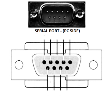
Figure 1. DB-9 connector

RS-232 Line Driver
- It consists of two-line drivers, two-line receivers, and a dual charge-pump circuit with ±15 kV ESD protection.
- It provides the electrical interface between an asynchronous communication controller and a serial port connector.
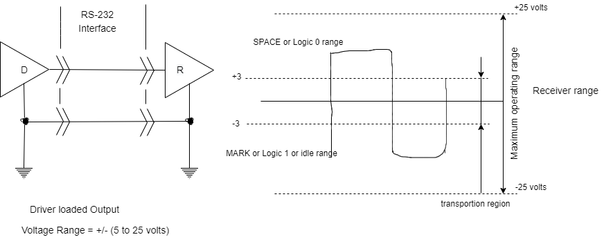
Figure 2. RS-232 Line Driver
- The maximum speed is 20kbit/s. However, modern equipment can operate much faster than this.
- The length of the cable also plays a part in maximum speed. The longer the cable and slower the speed you can obtain accurate results.
Q9) What is the main drawback of RS-232. What replaces RS-232 for better performance?
A9)
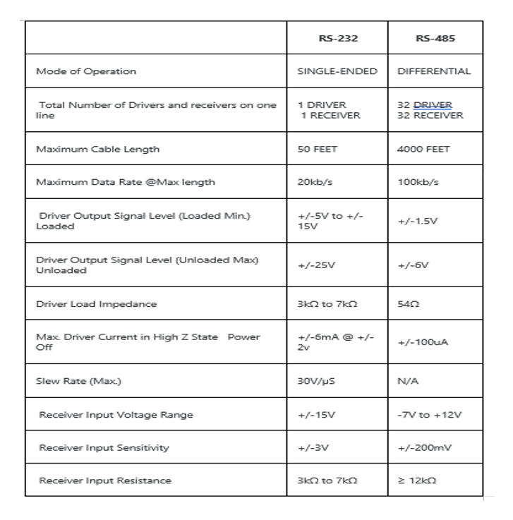
- The main drawbacks with RS-232 is lack of immunity for noise on the signal lines.
- The transmitter and receiver compare the voltages of data and handshake lines with one common zero line.
- The shifts in ground level produce disastrous effects. Therefore, the trigger level of RS-232 interface is set relatively high at ± 3V.
- In RS485 there is no common zero as signal reference. Several volts difference in ground level of RS485 transmitter and receiver does cause any problem.
- The RS485 signals are floating and each signal is transmitted over a Sig+ line and a Sig- line. The RS485 receiver compares the voltage difference between both lines,
- This works well and prevents the existence of ground loops, a common source of communication problems. The best results are achieved if the Sig+ and Sig- lines are twisted.
Q10) Explain transmission of I2C data transmission?
A10)
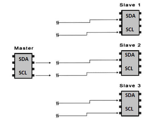
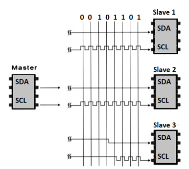
1. The master sends the start condition to every connected slave by switching the SDA line from a high voltage level to a low voltage level before switching the SCL line from high to low:
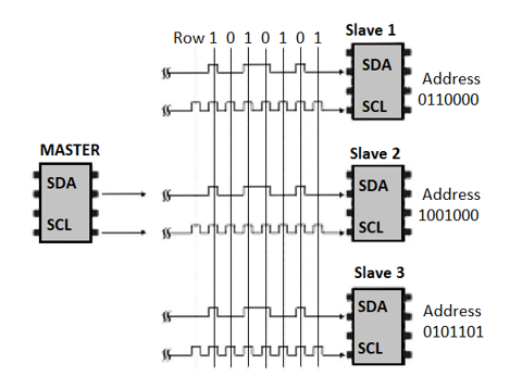
2. The master sends each slave the 7 or 10 bit address of the slave it wants to communicate with, along with the read/write bit:
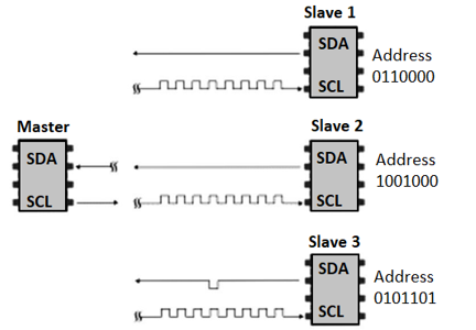
3. Each slave compares the address sent from the master to its own address. If the address matches, the slave returns an ACK bit by pulling the SDA line low for one bit. If the address from the master does not match the slave’s own address, the slave leaves the SDA line high.
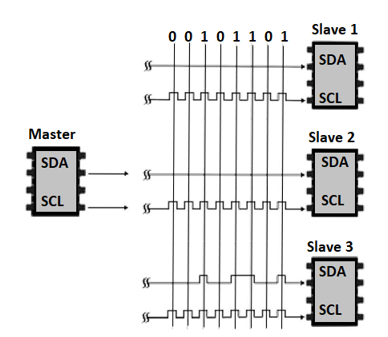
4. The master sends or receives the data frame:
5. After each data frame has been transferred, the receiving device returns another ACK bit to the sender to acknowledge successful receipt of the frame:
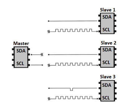
6. To stop the data transmission, the master sends a stop condition to the slave by switching SCL high before switching SDA high:
Q11) Explain what is serial peripheral interface?
A11)
- Serial Peripheral Interface (SPI) is an interface bus used to send data between microcontrollers and small peripherals such as shift registers, sensors, and SD cards. It uses separate clock and data lines, along with a select line to choose the device to talk to.
- SPI has a "synchronous" data bus, which means that it uses separate lines for data and a "clock" that keeps both sides in perfect sync.
- The clock is an oscillating signal which tells the receiver exactly when to sample the bits on the data line. This could be the rising (low to high) or falling (high to low) edge of the clock signal. When the receiver detects that edge, it will immediately look at the data line to read the next bit. Because the clock is sent along with the data.
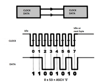
Figure 4. SPI
In SPI, only one side generates the clock signal called SCK for Serial ClocK. The side that generates the clock is called the "master", and the other side is called the "slave". There is always only one master, but there can be multiple slaves.
When data is sent from the master to a slave, it's sent on a data line called MOSI, for "Master Out / Slave In". If the slave needs to send a response back to the master, the master will continue to generate a prearranged number of clock cycles, and the slave will put the data onto a third data line called MISO, for "Master In / Slave Out".
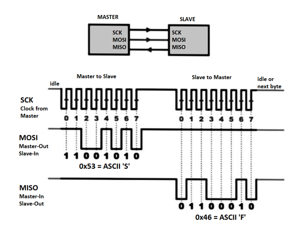
Figure 5. Master-Slave
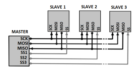
Figure 6. Multiple Slave
Q12) What is SPI read and write protocol?
A12)
SPI Read and Write Protocol.
- In connecting a device with an SPI bus to µC we use µC as the master and SPI device acts as slave.
- µC generates SCLK fed to SCLK pin of SPI to synchronize transfer of data one bit at a time. MSB goes in first.
- During transfer , the SS pin must be HIGH.
- To distinguish between read and write D7 bit of address byte is 1 and for read it is low.
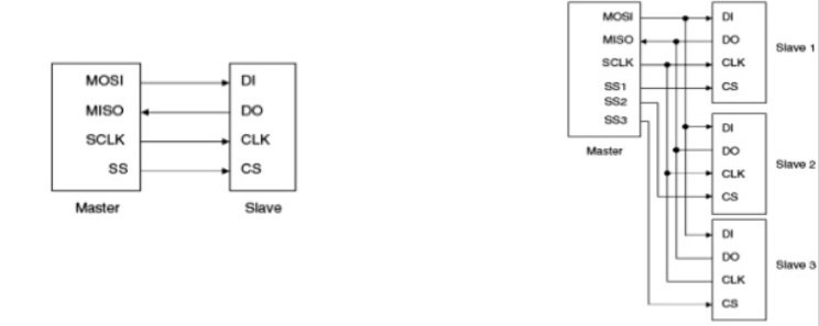
Figure 7. SPI Read Write Protocol
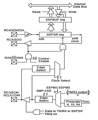
Figure 8. Registers.
The MSSP module has four registers for SPI mode operation. These are:
- MSSP control register (SSPCON1)
- MSSP status register (SSPSTAT)
- Serial receive/Transmit Buffer (SSPBUF)
- MSSP Shift register (SSPSR)
Q13) Write short notes on USART?
A13)
8251 universal synchronous asynchronous receiver transmitter (USART) acts as a mediator between microprocessor and peripheral to transmit serial data into parallel form and vice versa.
- It takes data serially from peripheral (outside devices) and converts into parallel data.
- After converting the data into parallel form, it transmits it to the CPU.
- Similarly, it receives parallel data from microprocessor and converts it into serial form.
- After converting data into serial form, it transmits it to outside device (peripheral).
Pin Configuration
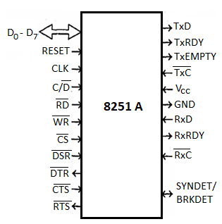
Fig 9 Pin Configuration
Data Bus: Bi-directional, tri-state, 8-bit Data Bus. This pin allows transfer of bytes between the CPU and the 8251A.
RD (Read): A low on this input allows the CPU to read data or status bytes from 8251A
WR (Write): A low on this input allows the CPU to write data or command word to the 8251A.
CLK (Clock): The CLK input is used to generate internal device timing. The frequency of CLK must be greater than 30 times the receiver or transmitter data bit rates.
RESET: A high on this input forces the 8251A into an “Idle” mode. The device will remain at “Idle” until a new set of control words is written into the 8251 Pin Diagram to program its functional definition.
C/D (Control /Data): This input in conjuction with the WR and RD inputs, informs the 8251A that the word on the Data Bus is either a data character control word or status information as shown in table.
C/ 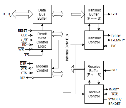  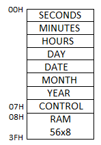 | Operation |
0 0 1 | CPU reads data from USART |
0 1 0 | CPU writes Data to USART |
1 0 1 | CPU reads Status from USART |
1 1 1 | CPU writes command to USART |
X 1 1 | USART Bus Floating |
CS (Chip Select): A low on this input allows communication between CPU and 8251A
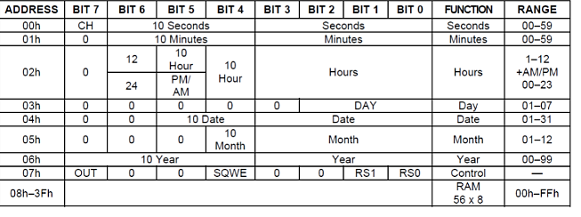
Fig 11 Block Diagram
It contains the following blocks:
- Data bus buffer –
This block helps in interfacing the internal data bus of 8251 to the system data bus. The data transmission is possible between 8251 and CPU by the data bus buffer block.
- Read/Write control logic –
It is a control block for overall device. It controls the overall working by selecting the operation to be done. The operation selection depends upon input signals as:

In this way, this unit selects one of the three registers- data buffer register, control register, status register.
- Modem control (modulator/demodulator) –
A device converts analog signals to digital signals and vice-versa and helps the computers to communicate over telephone lines or cable wires. The following are active-low pins of Modem.
- DSR: Data Set Ready signal is an input signal.
- DTR: Data terminal Ready is an output signal.
- CTS: It is an input signal which controls the data transmit circuit.
RTS: It is an output signal which is used to set the status RTS.
- Transmit buffer –
This block is used for parallel to serial converter that receives a parallel byte for conversion into serial signal and further transmission onto the common channel.
- TXD: It is an output signal, if its value is one, means transmitter will transmit the data.
- Transmit control –
This block is used to control the data transmission with the help of following pins:
- TXRDY: It means transmitter is ready to transmit data character.
- TXEMPTY: An output signal which indicates that TXEMPTY pin has transmitted all the data characters and transmitter is empty now.
- TXC: An active-low input pin which controls the data transmission rate of transmitted data.
- Receive buffer –
This block acts as a buffer for the received data.
- RXD: An input signal which receives the data.
- Receive control –
This block controls the receiving data.
- RXRDY: An input signal indicates that it is ready to receive the data.
- RXC: An active-low input signal which controls the data transmission rate of received data.
Q14) WAP in C for Initialization of I2C Module in Master Mode (I2C)
A14)
- Configure SCL and SDA pins as input through TRIS Register
- Calculate and Load Baud rate value in SSPADD for I2C Clock = 100Khz
SSPADD = ((Fosc/(4-112C Clock)) - 1 - Enable Master I2C mode in SSPCON1 register
SSPM3:SSPM0=1000 - I2C Master mode, clock=FOSC/(4 (SSPADD+1)) - Disable Slew rate control by setting SNIP bit in SSPSTAT in baud rate selected is standard (100 KHz and 1MHz)
- Enable I2C in SSPCON1 register by setting SSPEN bit in SSPCON1
Void i2C0_init()
{
TRISCbits.RC4=1; //Setting up SDA pins as inputs
TRISCbits.RC3=0; // SETTING SCL pin as output
SSPCON1 = 0x08; //i2C Master mode, clock = FOSC/(4 * (SSPADD + 1))
SSPSTATbits.SMP=1; //Enabling slew control for high sped mode
SSPADD= SSPADD_VAL; //Setting I2C clock
SSPCON1bits.SSPEN=1;//Enabling MSSP module
}
Q15) Write steps to write data to a slave device in interfacing of RTC?
A15)
- Send a start sequence by setting SEN bit in SSPCON2
- Check the start sequence transmitted
- Send the I'C address of the slave with the R/W bit Low (Even Address).SSPBUF = Slave Address
- Check the ACKSTAT from SSPSTAT
- Send the internal register/memory location address to which you want to write the data. SSPBUF = Address of register/memory location
- Send the data byte. SSPBUF = Data to be transmitted
- Check the ACKSTAT from SSPSTAT
- Send the stop sequence by setting PEN bit in SPPCON
Q16) Explain the RTC and RAM address map?
A16)
RTC and RAM address map

The address map for the RTC and RAM registers of the DS1307 are shown, The RTC registers are in address locations
- Ooh to 07h. The RAM registers are in address locations 08h to 3Fh. During a multi-byte access, when the address pointer reaches 3Fh, the end of RAM space, it wraps around to location Ooh, the beginning of the clock space.
RTC clock
Q17) Explain the write operation in RTC interfacing?
A17)
Write Operation:
- Serial data and clock are received through SDA and SCL.
- After each byte is received an acknowledge bit is transmitted.
- START and STOP conditions are recognized as the beginning and end of a serial transfer. Hardware performs address recognition after reception of the slave address and direction bit (see Figure).
- The slave address byte is the first byte received after the master generates the START condition.
- The slave address byte contains the 7-bit DS1307 address, which is 1101000, followed by the direction bit (R/W), which for a write is 0.
- After receiving and decoding the slave address byte, the DS1307 outputs an acknowledge on SDA. After the DS1307 acknowledges the slave address + write bit, the master transmits a word address to the DS1307.
- This sets the register pointer on the DS1307, with the DS1307 acknowledging the transfer.
- The master can then transmit zero or more bytes of data with the DS1307 acknowledging each byte received.
- The register pointer automatically increments after each data byte are written.
- The master will generate a STOP condition to terminate the data write.
Q18) Explain read operation steps in RTC interfacing?
A18)
Read Operation:
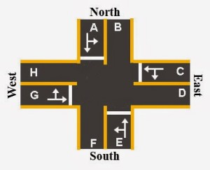
Fig 10 Write memory pointer
- The first byte is received and handled as in the slave receiver mode. However, in this mode, the direction bit will indicate that the transfer direction is reversed.
- The DS1307 transmits serial data on SDA while the serial clock is input on SCL.
- START and STOP conditions are recognized as the beginning and end of a serial transfer (see Figure).
- The slave address byte is the first byte received after the START condition is generated by the master. The slave address byte contains the 7-bit DS1307 address, which is 1101000, followed by the direction bit (R/W), which is 1 for a read.
- After receiving and decoding the slave address the DS1307 outputs an acknowledge on SDA.
- The DS1307 then begins to transmit data starting with the register address pointed to by the register pointer. If the register pointer is not written to before the initiation of a read mode the first address that is read is the last one stored in the register pointer.
- The register pointer automatically increments after each byte are read.
- The DS1307 must receive a Not Acknowledge to end a read.
Q19) Explain the design of four way traffic light system design steps?
A19)
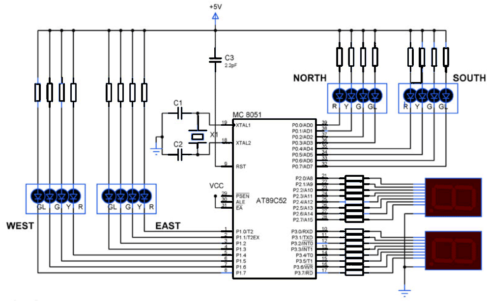
In this section we design the four-way traffic light system. This system is having a microcontroller and 7-segment LED for indications. The traffic flow is kept in mind while designing the TLC. The timings between each light need be to very precise and accurate. The LED s connected to the microcontroller using Common Anode configuration. When there is logic 0 signal in microcontroller the LED is ON and vice versa. We can use 12MHz crystal with microcontroller. In this case we are using 6MHz.

Figure 11 Traffic Light Controller

Figure 12 LED
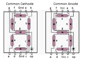
The above is shown circuit diagram for the Traffic light controller assembly having microcontroller and LED segments. The 7-segment should be connected to the port in the following order P2.0 to pin “a” of the 7 segment, P2.1 to b, P2.2 to c and ends up with P2.7 to h. These are the connection configurations and components we are going to use in this 4-way Traffic light system using 8051 Microcontroller.

Figure 13 Design for all four directions
A model for four-way road is shown above. The designing is done by considering this model. We consider North a starting point of the traffic. We need to consider only two directions straight and left as a free right turn is allowed in the design. The green signal according to our design needs to allow vehicles to go forward and to the left. We consider four zones mentioned below.
ZONE I-
We assume vehicles which are coming from A wants to travel to F through roads E to B. In order to achieve this green signal in A and E allows the traffic flow, while other directions are RED.
ZONE II-
In this zone traffic from G to D and C to H road is allowed. TO achieve this traffic from other directions is stopped by RED light.
ZONE III-
The traffic to the left from A to D and from E to H is allowed. The RED signal is shown to East and West directions.
ZONE IV-
Here traffic from G to B and C to F are allowed. The RED signal is active for North and South direction. To manage the traffic all the zone rules are repeated in sequence.
We need to make a note of the timings for the lights to be ON or OFF. It is completely based on the traffic and the design requirement. We consider here 50sec ON for RED light, 10 sec for yellow. Before switching the traffic flow for next zone, the green remains on for total of 60sec.
Q20) Explain read and write status registers of EEPROM with SPI?
A20)
READ STATUS REGISTER (RDSR): The Read Status Register instruction provides access to the status register. The Ready/Busy and Write Enable status of the device can be determined by the RDSR instruction. Similarly, the Block Write Protection bits indicate the extent of protection employed. These bits are set by using the WRSR instruction.

WRITE STATUS REGISTER (WRSR): The WRSR instruction allows the user to select one of four levels of protection.
The AT25128/256 is divided into four array segments. Top quarter (1/4), top half (1/2), or all of the memory segments can be protected. Any of the data within any selected segment will therefore be READ only.The block write protection levels and corresponding status register control bits are shown in Table 1.2.The three bits, BP0, BP1, and WPEN are nonvolatile cells that have the same properties and functions as the regular memory cells (e.g. WREN, tWC, RDSR).
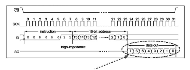
Figure 14 Instruction set for 25CXX for SPI EEPROM
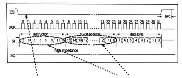
Figure 15 Block Write Protect bits.


Figure 16 Read Sequence
Upon completion, any data on the SI line will be ignored. The data (D7 – D0) at the specified address is then shifted out onto the SO line. If only one byte is to be read, the CS line should be driven high after the data comes out. The read sequence can be continued since the byte address is automatically incremented and data will continue to be shifted out. When the highest address is reached, the address counter will roll over to the lowest address allowing the entire memory to be read in one continuous read cycle.
Write Sequence:
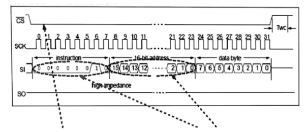
Figure 17 Write Sequence
Programming will start after the CS pin is brought high. The low-to-high transition of the CS pin must occur during the SCK low time immediately after clocking in the D0 (LSB) data bit. The Ready/Busy status of the device can be determined by initiating a Read Status Register (RDSR) instruction. If Bit 0 = “1”, the write cycle is still in progress. If Bit 0 = “0”, the write cycle has ended. Only the RDSR instruction is enabled during the write programming cycle.
