Unit - 2
Data Acquisition and Signal Communication
Q1) A modulating signal m(t)=10cos(2π×103t) is amplitude modulated with a carrier signal c(t)=50cos(2π×105t). Find the modulation index, the carrier power, and the power required for transmitting AM wave.
A1) Given, the equation of modulating signal as
m(t)=10cos(2π×103t)
We know the standard equation of modulating signal as
m(t)=Amcos(2πfmt)
Comparing both equations, we get
Amplitude of modulating signal as Am=10volts
And Frequency of modulating signal as fm=103Hz=1KHz
c(t)=50cos(2π×105t)
Comparing these two equations, we will get
Amplitude of carrier signal as Ac=50volts
And Frequency of carrier signal as fc=105Hz=100KHz
μ = Am/Ac
μ = 10/50 =0.2
The value of modulation index is 0.2
Carrier power, Pc
Pc=Ac2/2R
Let R=1ohm
Carrier power, Pc is 1250 watts.


Q2) The equation of amplitude wave is given by s(t)=20[1+0.8cos(2π×103t)] cos(4π×105t). Find the carrier power, the total sideband power, and the band width of AM wave.
A2) s(t)=20[1+0.8cos(2π×103t)] cos(4π×105t).
We can write above equation as
s(t)=20[1+0.8cos(2π×103t)] cos (4πx 2 x105t).
 t)
t)
Amplitude of carrier signal as Ac=20volts
Modulation index as μ=0.8
Frequency of modulating signal as fm=103Hz=1KHz
Frequency of carrier signal as fc=2×10⁵Hz=200KHz
The formula for Carrier power, Pc
Pc=Ac2/2R
Pc = (20)2/2(1) = 200W
Total side band power is
PSB=Pcμ2/2
PSB=200×(0.8)2/2=64W
Total side band power is 64 watts.
We know the formula for bandwidth of AM wave is
BW=2fm
Substitute fm value in the above formula.
BW=2(1K) =2KHz
The bandwidth of AM wave is 2 KHz.
Q3) A carrier is phase modulated (PM) with frequency deviation of 10 kHz by a single tone frequency of 1 kHz. If the single tone frequency is increased to 2 kHz, assuming that phase deviation remains unchanged the bandwidth of the PM signal is
A3)
- In PM phase deviation,


- If the frequency
 is increased to 2 kHz and phase deviation remains unchanged
 - The modulation index

- According to carsons rule
- Bandwidth=

Q4) A device with input 𝑥(𝑡) and output 𝑦(𝑡) is characterized by: 𝑦(𝑡)=𝑥2 (𝑡). An FM signal with frequency deviation of 90 KHz and modulating signal bandwidth of 5 KHz is applied to this device. The bandwidth of the output signal is (a) 370 KHz (b) 190 KHz (c) 380 KHz (d) 95 KHz
A4) Frequency deviation Δ𝒇=𝟗𝟎𝑲𝑯𝒛
Modulating signal bandwidth = 5 KMz
When FM signal is applied to doubler frequency deviation doubles.
𝑩.𝑾 = 𝟐(Δ𝒇+𝒇𝒎) = 𝟐(𝟏𝟖𝟎+𝟓) =𝟑𝟕𝟎 𝑲𝑯z
Q5) An FM signal with a modulation index 9 is applied to a frequency tripler. The modulation index in the output signal will be (a) 0 (b) 3 (c) 9 (d) 27
A5) The frequency modulation index β is multiplied by n in n-times frequency multiplier.
𝑺𝒐, 𝜷′=𝟑×𝟗 = 27
Q6) A sinusoidal modulating waveform of amplitude 5 V and a frequency of 2 KHz is applied to FM generator, which has a frequency sensitivity of 40 Hz/volt. Calculate the frequency deviation, modulation index, and bandwidth.
A6) Given, the amplitude of modulating signal, Am=5V
Frequency of modulating signal, fm=2KHz
Frequency sensitivity, kf=40Hz/volt
We know the formula for Frequency deviation as
Δf=kfAm
Δf=40×5=200Hz
β=Δf/fm
β=200/(2×1000) = 0.1
The formula for Bandwidth of Narrow Band FM is the same as that of AM wave.
BW=2fm
BW=2×2K=4KHz
Q7) An FM wave is given by s(t)=20cos(8π×106t+9sin(2π×103t)). Calculate the frequency deviation, bandwidth, and power of FM wave.
A7) s(t)=20cos(8π×106t+9sin(2π×103t))
We know the standard equation of an FM wave as
s(t)=Accos(2πfct+βsin(2πfmt))
Amplitude of the carrier signal, Ac=20V
Frequency of the carrier signal, fc=4×10⁶Hz=4MHz
Frequency of the message signal, fm=1×10³Hz=1KHz
Modulation index, β=9
β=Δf/fm
Δf=9×1K=9KHz
The formula for Bandwidth of Wide Band FM wave is
BW=2(β+1)fm
BW=2(9+1)1K=20KHz
The bandwidth of Wide Band FM wave is 20KHz
Pc=Ac2/2R
P= (20)2/2(1) =200W
Therefore, the power of FM wave is 200watts.
Q8) In a summing amplifier, if R = 1kΩ, Va = +3V, Vb = +8V, Vc = +9V, Vd = +5V and supply voltage is ±15V. Find the output voltage Vo.
A8) Vo = Sum of all input voltages applied at both the terminals
Vo = Va + Vb + Vc +Vd
Vo = -3 -8 +9 +5
Vo = +3V
Q9) Find the output voltage for the given circuit diagram if Rf = 5kΩ.
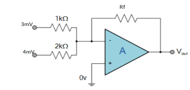
A9)
We know,
Gain (Av) = =
= 
Hence,
Av1 = 
Av2 = 
Now, Output voltage Vo = Sum of the two amplified input signals
Vo = Av1 x V1 + Av2 x V2
Vo =(-5 x 3) + ( -2.5x 4) mV
Vo = -25mV
As the above output voltage is negative hence it is an inverting amplifier.
Q10) A 200mV peak to peak sine waveform voltage is applied to Op-amp inverting amplifier with Rf/R1 = 10.
A10) Peak to peak input voltage
2Vm = 200 mV
Vm = 100 mV
Vi= Vm sin wt = 100 sin wt mV
Vo = -Rf/R1 x vi = -10 x 100 sinwt mV
= -1000 sin wt mV
Q11) Design a non-inverting amplifier using Op-amp with a closed loop voltage gain of 10.
A11)
Af = 1 + Rf/R1 =10
Rf/R1 = 9
Rf = 9 R1
If R1 = 1K
Rf = 9K Ω
Q12) In an op-amp inverting amplifier R1 = 1K Ω and Rf = 100KΩ. The DC supply voltage of the op-amp is ± 15V. Calculate the output voltage if input voltage is 1V.
A12)
R1 = 1KΩ Rf = 100KΩ
V+ = 15V and V-=-15V. Vi = 1V
Af = -Rf/R1 = -100K/1K = -100
Af = vo/vi
Vo = Af vi
= -100 x 1V = -100V
The output voltage cannot exceed the DC power supply voltage. Since vo is negative and large it is limited to V-
Vo ≈ V- = -15V
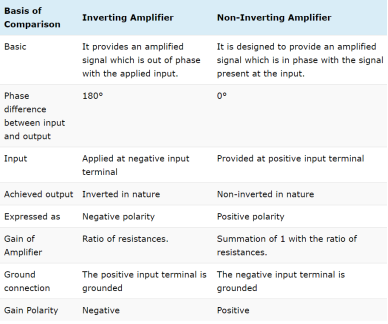
Q13) Compare inverting, non-inverting and differential amplifier?
A13)
Q14) Explain synchronous and asynchronous types of communications?
A14) Types of Communication system
1)Synchronous transmission
In synchronous transmission, data moves in a completely paired approach, in the form of chunks or frames. Synchronisation between the source and target is required so that the source knows where the new byte begins, since there are no spaces included between the data. Synchronous transmission is effective, dependable, and often utilised for transmitting a large amount of data. It offers real-time communication between linked devices.An example of synchronous transmission would be the transfer of a large text file. Before the file is transmitted, it is first dissected into blocks of sentences. The blocks are then transferred over the communication link to the target location.
Characteristics of Synchronous Transmission
- There are no spaces in between characters being sent.
- Timing is provided by modems or other devices at the end of the transmission.
- Special ’syn’ characters go before the data being sent.
- The syn characters are included between chunks of data for timing functions.
Examples of Synchronous Transmission
- Chatrooms
- Video conferencing
- Telephonic conversations
- Face-to-face interactions
2)Asynchronous Transmission
In asynchronous transmission, data moves in a half-paired approach, 1 byte or 1 character at a time. It sends the data in a constant current of bytes. The size of a character transmitted is 8 bits, with a parity bit added both at the beginning and at the end, making it a total of 10 bits. It doesn’t need a clock for integration—rather, it utilises the parity bits to tell the receiver how to translate the data.It is straightforward, quick, cost-effective, and doesn’t need 2-way communication to function.
Characteristics of Asynchronous Transmission
Serial vs Parallel Communication | |
The process of sending data one bit at a time, sequentially over a communication channel or a computer bus. | The process of sending multiple bits as a whole on a link with several parallel channels or computer buses. |
Required Number of Lines | |
Uses a single line to send data | Uses several lines to transmit data |
Speed | |
Slow for short distances and low frequencies but higher in long distances and high frequencies | Fast for short distance and low frequencies but slower in long distances and high frequencies |
Error and Noise | |
Error and Noise are minimum | Error and noise are high |
Nature | |
Simple and straightforward | Unreliable and complicated |
Cost | |
Cost is comparatively lower | Cost is higher in comparison |
- Each character is headed by a beginning bit and concluded with one or more end bits.
- There may be gaps or spaces in between characters.
Examples of Asynchronous Transmission
- Emails
- Forums
- Letters
- Radios
- Televisions
Q15) Write short notes on programmable control amplifier?
A15) Programmable gain amplifiers are typically non-inverting operational amplifiers with a digitally controlled analog switch connected to several resistors in its feedback loop. An external computer or another logic or binary signal controls the addressable inputs of the analog switch so it selects a certain resistor for particular gain. The data acquisition system’s signal conditioners sense the input signal amplitude and automatically send the proper binary code to the programmable gain amplifier (PGA) to increase the gain for a low signal, or decrease the gain for a large signal. The input signal then can be measured and displayed without distortion.
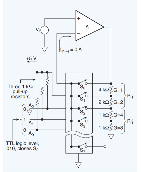
Fig: Programmable gain Amplifier
Q16) Explain instrumentation amplifier with circuit diagram?
A16) The Instrumentation amplifiers consist of three op-amps. In this circuit, a non-inverting amplifier is connected to each input of the differential amplifier.
This instrumentation amplifier provides high input impedance for exact measurement of input data from transducers. The circuit diagram of an instrumentation amplifier is as shown in the figure below.
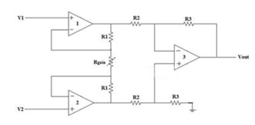
Fig: Instrumentation Amplifier
The op-amps 1 & 2 are non-inverting amplifiers and together form an input stage of the instrumentation amplifier. The op-amp 3 is a difference amplifier that forms the output stage of the instrumentation amplifier.
Working
The output stage of the instrumentation amplifier is a difference amplifier, whose output Vout is the amplified difference of the input signals applied to its input terminals.
If the outputs of op-amp 1 and op-amp 2 are Vo1 and Vo2 respectively, then the output of the difference amplifier is given by,
Vout = (R3/R2)(Vo1-Vo2)
The expressions for Vo1 and Vo2 can be found in terms of the input voltages and resistances.
Consider the input stage of the instrumentation amplifier as shown in the figure below.
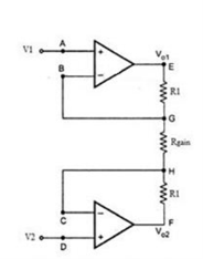
Fig: Input Stage of Instrumentation Amplifier
The potential at node A is the input voltage V1. Hence the potential at node B is also V1, from the virtual short concept. Thus, the potential at node G is also V1.
The potential at node D is the input voltage V2. Hence the potential at node C is also V2, from the virtual short. Thus, the potential at node H is also V2.
Ideally the current to the input stage op-amps is zero. Therefore, the current I through the resistors R1, Rgain and R1 remains the same.
Applying Ohm’s law between the nodes E and F,
I = (Vo1-Vo2)/(R1+Rgain+R1) ——————— 1
I = (Vo1-Vo2)/(2R1+Rgain)
Since no current is flowing to the input of the op-amps 1 & 2, the current I between the nodes G and H can be given as,
I = (VG-VH)/Rgain = (V1-V2)/Rgain ————————- 2
Equating equations 1 and 2,
(Vo1-Vo2)/(2R1+Rgain) = (V1-V2)/Rgain
(Vo1-Vo2) = (2R1+Rgain) (V1-V2)/Rgain —————— 3
The output of the difference amplifier is given as,
Vout = (R3/R2) (Vo1-Vo2)
Therefore, (Vo1 – Vo2) = (R2/R3)Vout
Substituting (Vo1 – Vo2) value in the equation 3, we get
(R2/R3)Vout = (2R1+Rgain)(V1-V2)/Rgain
i.e. Vout = (R3/R2) {(2R1+Rgain)/Rgain} (V1-V2)
The above equation gives the output voltage of an instrumentation amplifier. The overall gain of the amplifier is given by the term (R3/R2) {(2R1+Rgain)/Rgain}.
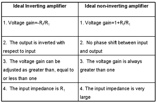
Q17) Compare inverting and non inverting amplifier?
A17)
Q18) Write short notes on quantization?
A18) Quantizing is defined as the transformation of a continuous analog input into a set of discrete output states. Quantization noise is a model of quantization error introduced by quantization in the analog-to-digital conversion (ADC). It is a rounding error between the analog input voltage to the ADC and the output digitized value. The noise is non-linear and signal-dependent.
An analog-to-digital converter is an electronic device that converts an analog voltage to a digital code. The output of the A/D converter can be directly interfaced to digital devices such as microcontrollers and computers. The resolution of an A/D converter is the number of bits used to digitally approximate the analog value of the input. The number of possible states N is equal to the number of bit combinations that can be output from the converter:
N=2n
Where n is the number of bits. For the example illustrated in Figure, the 3-bit device has 23 or 8 output states as listed in the first column. The output states are
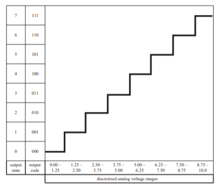
Fig: A/D conversion
Usually numbered consecutively from 0 to (N- 1). The corresponding code word for each output state is listed in the second column. Most commercial A/D converters are 8-, 10-, or 12-bit devices that resolve 256, 1024, and 4096 output states, respectively. The number of analog decision points that occur in the process of quantizing is (N- 1). In Figure above, the decision points occur at 1.25 V, 2.50 V, . . . , and 8.75 V. The analog quantization size Q, sometimes called the code width, is defined as the full-scale range of the A/D converter divided by the number of output states
Q=(Vmax-Vmin)/N
It is a measure of the analog change that can be resolved by the converter. Although the term resolution is defined as the number of output bits from an A/D converter, sometimes it is used to refer to the analog quantization size. For our example, the analog quantization size is 10/8 V 1.25 V. This means that the amplitude of the digitized signal has an error of at most 1.25 V. Therefore, the A/D converter can only resolve a voltage to within 1.25 V of the exact analog voltage.
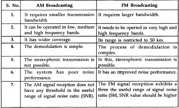
Q19) List difference between AM/FM?
A19)
