Unit 1
- Explain p-type and n-type semiconductor?
N type Semiconductor:-
To increase the number of conduction band electrons inintrisic silicon , pentavalent imparity atoms are added. These are atoms with five valence electrons such as
i) arsenic (as)
Ii) phosphors (p)
Iii) Bismuth (Bi)
Iii) Antimony ( sb)
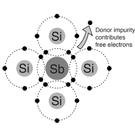
- Pentavalent impurity atom in a silicon crystal. An antimony (sb) impurity atom shown above-
- Each pentavalent atom forms covalent bonds with four adjustment silicon atoms, leaving one extra electron.
- The pentavalent atom gives up on electron, it often called a donor atom.
- Majority and minority carriers: - A type here means negative charge of an electron. Electron are called the majority carriers in n-type material.
- Hole in an n-type material are called minority carriers
P Type Semiconductor :-
To increase the number of holes in intrinsic silicon trivalent impurity atoms are added these are atoms with their valence electrons such as
i) Baron(B)
Ii) Indium(IN)
iii)Gallium(GO)
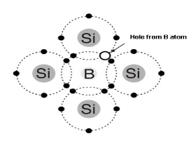
- Trivalent impurity atom in a silicon crystal structure. A) boron (B) impurity atom is shown in the center.
- The number of holes can be carefully controlled by the number of trivalent impurity atoms added to the silicon .
- A Hole created by the doping process is not accompanied by a conduction (free) electron.
- Trivalent Atom can take an electron it is often referred to as on accepted atom
2. Explain half-wave rectifier?
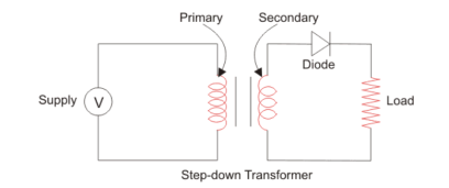
First, a high AC voltage is applied to the to the primary side of the step down transformer and a low voltage at the secondary winding obtained is applied to the diode.

During the positive half cycle of the AC voltage, the diode will be forward biased and the current flows through the diode. During the negative half cycle of the AC voltage, the diode will be reverse biased and the flow of current will be blocked. The final output voltage waveform on the secondary side (DC) is shown in figure
If we replace the secondary transformer coils with a source voltage, we can simplify the circuit diagram of the half-wave rectifier as:

For the positive half cycle of the AC source voltage, the equivalent circuit effectively becomes:
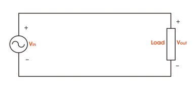
This is because the diode is forward biased, and is hence allowing current to pass through. So we have a closed circuit.
But for the negative half cycle of the AC source voltage, the equivalent circuit becomes:
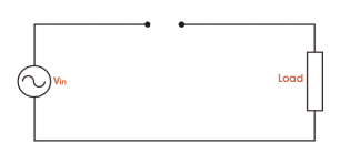
Because the diode is now in reverse bias mode, no current is able to pass through it. As such, we now have an open circuit. Since current can not flow through to the load during this time, the output voltage is equal to zero.
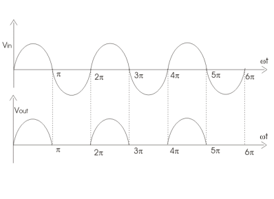
The half wave rectifier waveform of input side (Vin), and the output side (Vout) after rectification (i.e. conversion from AC to DC):
3. Explain centre-tapped full wave rectifier?
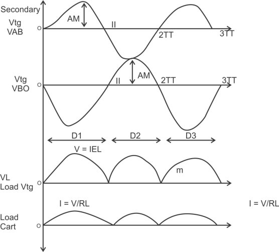
A center tapped rectifier is a type of full wave rectifier that uses two diode connected to the secondary of a center tapped transformer.
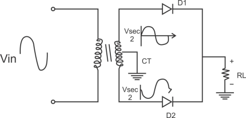
Center tapped full wave rectifier operation:-
I) During positive half cycle of i/p ac supply.
Diagram

D1.Is in forward biased & D2 is in reverse biased.
II)During -ve half cycle.

D1 Reverse biased
D2 Forward biased
4. Explain bridge rectifier?
The bridge rectifier uses four diode connected, when the i/p cycle is positive diode D1 & D2 are forward biased and conduct current in the direction shown a vtg is developed across RL which looks the positive half of the i/p cycle during this diodes D3 and D4 are reverse biased.
When the ilp cycle is -ve diode D3& D4 are forward biased & conduct current in the same direction through R1 as during in the positive half cycle during the -ve half cycle D1& D2 are reverse biased. a full wave rectified O/P VTG appears across RL as a result of this action.
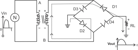
- during positive half cycle of ilp D1 & D2 are forward biased conduct current D3 & D4 are reverse biased:-
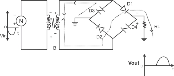
- during -ve half cycle of the ilp D3 &D4 are forward biased & conduct current D1 & D2 are reverse biased-
5. Explain voltage regulator using Zener diodes?
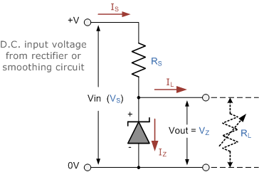
Resistor, RS is connected in series with the zener diode to limit the current flow through the diode with the voltage source, VS being connected across the combination. The stabilised output voltage Vout is taken from across the zener diode.
The zener diode is connected with its cathode terminal connected to the positive rail of the DC supply so it is reverse biased and will be operating in its breakdown condition. Resistor RS is selected so to limit the maximum current flowing in the circuit.
With no load connected to the circuit, the load current will be zero, ( IL = 0 ), and all the circuit current passes through the zener diode which in turn dissipates its maximum power.
Also a small value of the series resistor RS will result in a greater diode current when the load resistance RL is connected and large as this will increase the power dissipation requirement of the diode so care must be taken when selecting the appropriate value of series resistance so that the zener’s maximum power rating is not exceeded under this no-load or high-impedance condition.
The load is connected in parallel with the zener diode, so the voltage across RL is always the same as the zener voltage, ( VR = VZ ).
There is a minimum zener current for which the stabilisation of the voltage is effective and the zener current must stay above this value operating under load within its breakdown region at all times.
The upper limit of current is of course dependant upon the power rating of the device. The supply voltage VS must be greater than VZ.
6. What is BJT ? Explain its operation?
The BJT is constructed with the three draped semiconductors region’s separate by two Pn junctions as shown below
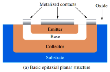
-Basic epitaxial planner structures.
-Three terminal with region’s are called emitter, base and collector.
-The physical representation of the two types of BJT’s,
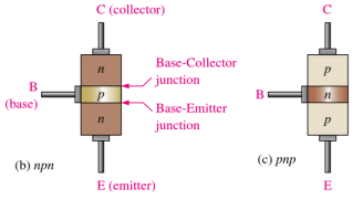
One type consists between two regions separated by a P region (npn) and other type consists of two p regions separated by an n region (pnp).
-The Pn junction joining the base region and the emitter region is called the base emitter junction.
-The Pn junction joining the base region and the collector region is called the base collector junction.
-The base region is lightly doped and very thin compared to the heavily doped emitter and the moderately doped collector regions.
*Base Transistor Operation:-
In order for the transistor to operate properly as an amplifier the two pn junction must be correctly biased with the external D.C vtg.
-The next figure shows the proper bias arrangement for both the npn and pnp transistors for active operation as an amplifier.
-In both the cases the base emitter
(BE) junction is forward biased & the base collector junction (BC) junction is reverse biased
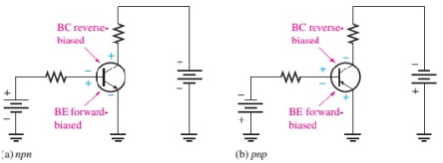
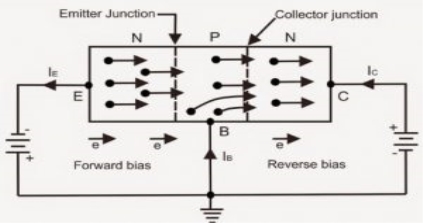
- As from above figure consider n-p-n transistor. The forward bias from base to emitter narrow’s the BE depletion region and the reverse bias from base to collector widens the BC depletion region shown in figure.
- The heavily doped N-TYPE emitter region is full with conduction band(frep) electron’s that easily diffuse through the forward biased BE junction into the p-type base region where they become minority carrier’s same as forward biased diode region
- The base region is lightly doped & very thin so that it has a very limited number of holes.
- Those only a small percentage of all the e-flowing the BE junction can combine with the available holes in the base.
- The relatively few recombined flow out of the base lead as valance electrons, forming as small base current.
- Most of the e flowing from the emitter into the thin lightly dooped base region do not recombine but diffuse into the BC depletion region.
- The BC depletion region diffuse e is being pulled across the reverse biased BC junction by the attraction of the collector supply vtg.
- The electrons now move through the collector region, out through the collector lead into the +ve terminal of the collector vtg source. This forms the collector electrons current.
- The collector current is much larger than the base current.
- This is the reason transistor exhibit current gain.
7. What are the configurations of transistor ?
Transistor’s Configuration:-
1) Common Base configuration(C.B)
2) Common emitter Configuration(C.E)
3) Common Collector Configuration(C.C)
8. Explain CB configuration?
Common Base configuration(C.B):-

-The I/p is applied between the emitter and the base. The base acts as a common terminal between the I/p and o/p.
-The input vtg is therefore VEB and the input current is IE.
-The output is taken between the collector and the base therefore the output vtg is VCB and the output current is IC.
* Current relation’s in CB configuration:-
-The collector current is IC of the common base configuration is given by
Ic=Ic(INI)+ICBO
-Where the Ic(INI) called the injected collectors current and it is due to the number of electrons crossing the collectors base junction.
-ICBO :- This is the reverse saturation current flowing due to the minority carrier’s between the collector and base when the emitter is open
-ICBO flow’s due to the reverse biased collector’s base junction. As ICBO negligible as compared to Ic(INI) we can neglect it in practice.
.’. Ic=Ic(INI)………………………practically
Ic=ICBO………………with emitter open
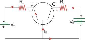
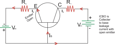
 Emitter is open
 ICBO
ICBO
Collector is to base control
-Since the ICBO flow’s due to terminally generated minority carrier’s it increases with increase the temperature.
-It doubles it’s value for every 100c rise in temperature.
-Current amplification factor or current gain (ddc):-
Current amplification factor or current gain is the ratio of collector current due to the injection to the total emitter current
αd.c = Ic(INI)
-The value of the ddc for CB configuration will always be less than 1.This is because
Ic(INI)<IE.
-Typically the value of d.d.c ranges between 0.95 to 0.995 depending upon the thickness of the base region.
-Larger the thickness of the base region smaller the value of the d.d.c
Ic(INI)=d.d.c.IE
Hence the expression for IC is given by
IC=αd.c IE + ICBo--------------------I
But the ICBo is negligibly small
IC d.d.c IE
* Expression for IB:-
IE=IB+IC
IE=αd.cIE+ICBo+IB…………………from I
IB=(1-αd.c)IE-ICBo
Neglecting ICBo
IB=(1-αd.c)IE
9. Explain the input and output configurations of CB?
1. Input Characteristic:-
A. Input Characteristic: is always a graph of input current verses input vtg. For common base (CB) configuration input current is the emitter current (IE) & I/p vtg. Is the emitter to the base vtg (VEB)
The I/p Characteristic is plotted at a constant O/p vtg. VCB
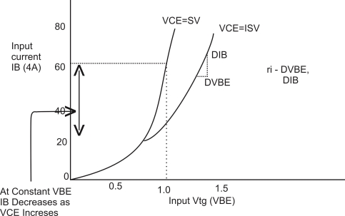
B. Output Characteristic:
Output Characteristic is always a graph of O/p current versus O/p Vtg.
For the CB configuration the O/p current is collector current (IC) of the output voltage is collector to base vtg. (VCB)
Output Characteristic is plotted for a constant value of I/p current (IE)
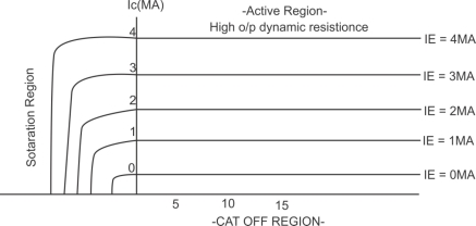
O/p Characteristic of a n-p-n transistor in CB Configuration
Dynamic O/p resistance (ro)
Ro =  / I
/ I  constant
In the active region Ic does not depend on VCB. It depends only on the I/p current IE. That is why the transistor is called as a current controlled or current operated device.
10. Explain saturation and cut-off region?
Saturation region is one in which both Emitter Base and Base Collector junctions of the transistor are forward biased. In this region high currents flows through the transistor, as both junctions of the transistor are forward biased and bulk resistance offered is very much less. Transistor in saturation region is considered as on state in digital logic.
A transistor is said to be in saturation if and only if
β > Ic/Ib
This is due to the fact that as both junctions of transistor are forward biased along with electron current flowing from emitter to base in active region there will be additional component of electron current flowing from collector to base.
Cutoff region
In this region both junctions of the transistor are reverse biased. Hence transistor in cut off does not conduct any currents expect for small reverse saturation currents that flow across junctions.
In cutoff condition emitter current is zero and the collector current consists of small reverse saturation currents.
The transistor when used as switch is operated in cutoff on condition and saturation regions which corresponds to switch off an on condition respectively.