Unit 1
8085
Q1) Explain the architeture of 8085?

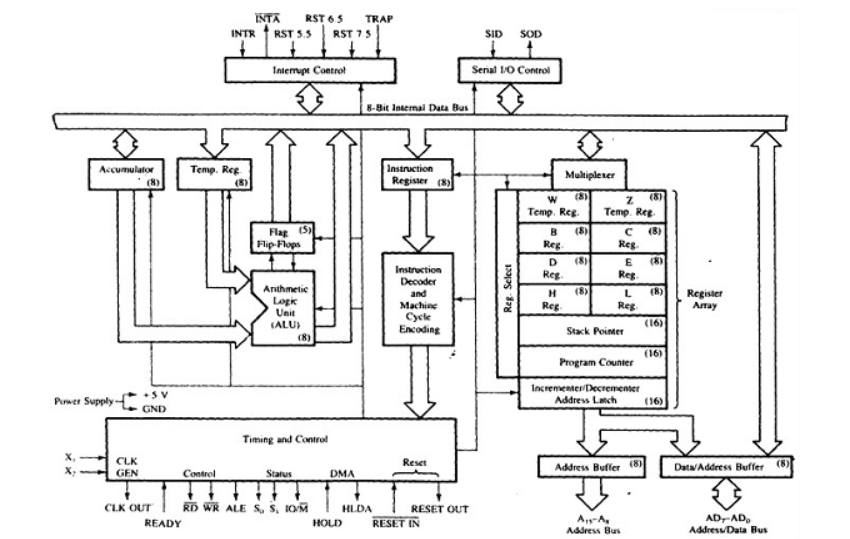
A1) 8085 consists of the following functional units −
Accumulator
The accumulator is an 8-bit register used to perform arithmetic, logical, I/O & LOAD/STORE operations. It is connected to internal data bus & ALU.
Arithmetic and logic unit
The arithmetic and logic unit performs arithmetic and logical operations like Addition, Subtraction, AND, OR, etc. on 8-bit data.
General purpose register
8085 consists of six general purpose registers in 8085 processor that is B, C, D, E, H & L. Each register holds 8-bit data. These registers work in pair to hold 16-bit data and their pairing combination is like B-C, D-E & H-L.
Program counter
It is a 16-bit register used to store the memory address location of the next instruction to be executed. Microprocessor increments the program whenever an instruction is being executed, so that the program counter points to the memory address of the next instruction that is going to be executed.
Stack pointer
It is 16-bit register which works like stack, which gets incremented/decremented by 2 during push & pop operations.
Temporary register
It is an 8-bit register, which holds the temporary data of arithmetic and logical operations.
Flag register
It is an 8-bit register which holds 0 or 1 depending upon the result stored in the accumulator.
These are : −

Instruction register and decoder
It is an 8-bit register. When an instruction is fetched from memory then it is stored in the Instruction register. Instruction decoder decodes the information present in the Instruction register.
Timing and control unit
It provides timing and control signal to the microprocessor to perform operations. Following are the timing and control signals, which control external and internal circuits −
Interrupt control
It controls the interrupts during the process. When the microprocessor is executing the main program and whenever an interrupt occurs, the microprocessor shifts the control from the main program to process the incoming request. After the request is completed, the control returns to the main program.
There are 5 interrupt signals in 8085 microprocessors:
Serial Input/output control
It controls the serial data communication by using the two instructions: SID (Serial input data) and SOD (Serial output data).
Address buffer and address-data buffer
The content stored in the stack pointer and program counter is loaded into the address buffer and address-data buffer to communicate with the CPU.
The memory and I/O chips are connected to these buses, the CPU can exchange the desired data with the memory and I/O chips.
Address bus and data bus
Data bus carries the data to be stored. It is bidirectional whereas address bus carries the location to where it should be stored, and it is unidirectional. It is used to transfer the data & Address I/O devices.
Q2) Explain the features of 8085?
A2)
1. It is an 8-bit microprocessor i.e. it can accept, process, or provide 8-bit data simultaneously.
2. It operates on a single +5V power supply connected at Vcc; power supply ground is connected to Vss.
3. It operates on clock cycle with 50% duty cycle.
4. It has on chip clock generator. This internal clock generator requires tuned circuit like LC, RC or crystal. The internal clock generator divides oscillator frequency by 2 and
generates clock signal, which can be used for synchronizing external devices.
5. It can operate with a 3 MHz clock frequency. The 8085A-2 version can operate at the maximum frequency of 5 MHz.
6. It has 16 address lines, hence it can access (216) 64 Kbytes of memory.
7. It provides 8 bit I/O addresses to access (28 ) 256 I/O ports.
8. In 8085, the lower 8-bit address bus (A0 – A7) and data bus (D0 – D7) are Multiplexed to reduce number of external pins. But due to this, external hardware (latch) is required to separate address lines and data lines.
Q3) What are the classifications of 8085 instructions?
A3) The Classification of Instruction Set of 8085 is categorised into five different groups:
Q4) Explain data transfer operations?
A4) The data transfer instructions load the data into register:
Therefore, we can say that data transfer instructions copy data from source to destination. The source can be data or contents of register or contents of memory location whereas destination can be register or memory location. These instructions do not affect the flag register of the processor.
Q5) Explain Arithmetic Operations?
A5) The arithmetic instructions perform addition, subtraction, increment and decrement operations.
Two registers cannot be added directly that is the contents of B and C registers cannot be added directly. To add two 16-bit numbers the 8085 provides DAD instruction. It adds the data within the register pair to the contents of the HL register pair and resulted sum is stored in the HL register pair.
Q6) Explain logical operations?
A6) The logical instructions perform logical, rotate, compare and complement operations.
Q7) Explain machine control operations?
A7) These instructions control the stack operations, input/output operations and machine operations. The stack instructions allow the transfer of data from register pair to stack memory and from stack memory to the register, pair.
The input/output instruction allows the transfer of 8-bit data to input/output port. Machine instructions control the Machine operations such as interrupt, halt, or do nothing.
Q8) Explain Data Transfer Instructions?
A8) Data Transfer Instruction
These instructions transfer data between registers or between memory and registers. The instruction is used to copy data from source to destination while copying the contents of source cannot be modified.


For example MOV B,C
MVI B,20H
LXI H, 4020H
LDA 6000H
Q9) Explain Arithmetic and Logical instructions?
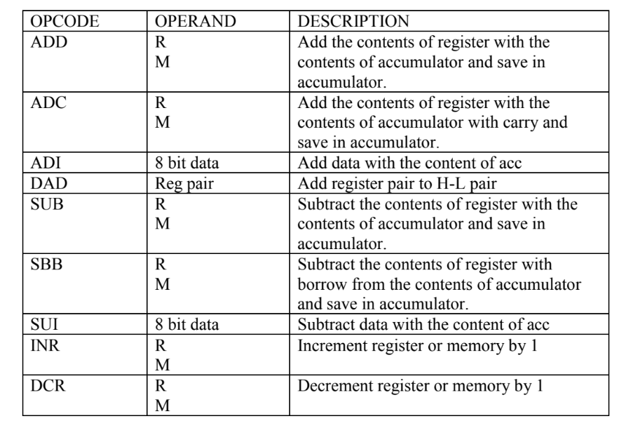
A9)

For example:
ADD C
ADC M
ADI 40H
DAD HL
SUB B
SUI 20H
INR C
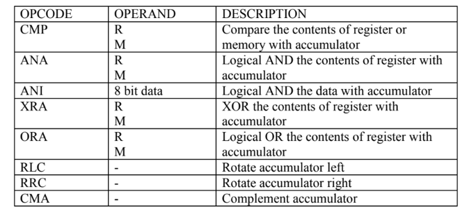
Logical Instructions
The logical operations are:

For example
CMP C
ANA B
ANI 40H
XRA M
ORA C
RLC
Q10) Explain branching instructions?
A10) These instructions alter the normal sequential flow conditionally or unconditionally
OPCODE | OPERAND | DESCRIPTION |
JMP | 16-bit address | Jump unconditionally to the given location |
JC | 16-bit address | Jump if carry |
JNC | 16-bit address | Jump if no carry |
JZ | 16-bit address | Jump if zero |
JNZ | 16-bit address | Jump if no zero |
CALL | 16-bit address | Call unconditionaly |
RET | 16-bit address | Return unconditionally |
RST | 16-bit address | Restart (Software Interrupts) |
For example
JMP 2000H
RET
RST 6
Q11) Briefly describe 8051 microcontroller?
A11) 8051 is the first most popular microcontroller known as MCS-51. It was introduced by Intel in the year 1981.
Initially it was N-type metal-oxide-semiconductor (NMOS) based microcontroller, but gradually versions were based on complementary metal-oxide-semiconductor (CMOS) technology. So, these microcontrollers were named as 80C51 where C it is based on CMOS technology.
It is an 8-bit microcontroller which means data bus is of 8-bits. Therefore, it can process 8-bits at a time. It is used in wide variety of embedded systems like robotics, remote controls, automotive industry, telecom applications, power tools etc.

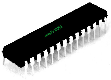
8051 Microcontroller
System on a Chip :
It is also referred to as System on a Chip (SoC) microcontroller because it is a chip circuit/integrated circuit that holds many components of a computer together on a single chip which include CPU, memory, input output ports(I/O ports), timers and secondary storage.