DC
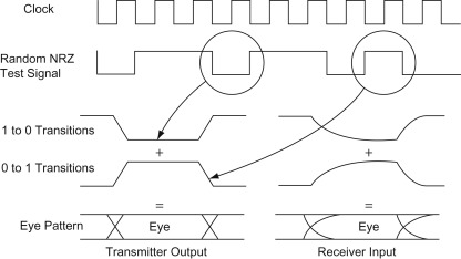
UNIT - 4Band pass Modulation & Demodulation Q1) Draw and explain eye diagram.A1) An eye diagram or eye pattern is simply a graphical display of a serial data signal with respect to time that shows a pattern that resembles an eye. The signal at the receiving end of the serial link is connected to an oscilloscope and the sweep rate is set so that one- or two-bit time periods (unit intervals or UI) are displayed. This causes bit periods to overlap and the eye pattern to form around the upper and lower signal levels and the rise and fall times. The eye pattern readily shows the rise and fall time lengthening and rounding as well as the horizontal jitter variation.
Fig.: eye diagram Q2) Compare ASK, PSK, FSK.
|
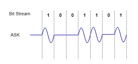
A2) Amplitude Shift Keying (ASK)In ASK, the amplitude of the signal is varied to represent the signal levels, while frequency and phase remains constant. In order to represent 0 and 1, two different amplitudes are used.
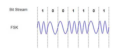
Fig.: ASK Frequency Shift Keying (FSK)In FSK, the frequency of the signal is modulated to represent the signal levels, while amplitude and phase remains constant. To represent the signal levels 0 and 1, two different frequencies are used.
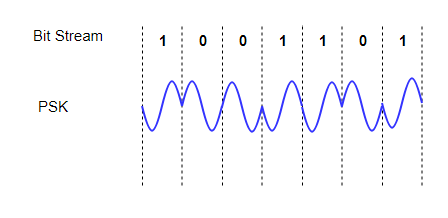
Fig.: FSK Phase Shift Keying (PSK)In this, the phase of the carrier signal is modulated to represent the signal levels, while amplitude and frequency remains constant. Binary Phase Shift Keying (BPSK) is the simplest form of PSK where there are two signal elements represented by two different phases.In Quadrature PSK (QPSK), two bits of information are transmitted per symbol by using four different phases.
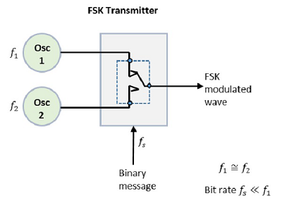
Fig.: PSK Q3) Explain FSK generation and detection.A3) FSK ModulatorThe FSK modulator block diagram comprises of two oscillators with a clock and the input binary sequence. Following is its block diagram.
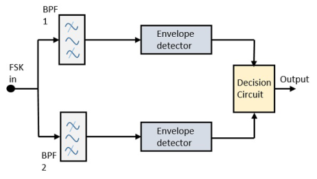
Fig.: FSK modulator The two oscillators, producing a higher and a lower frequency signals, are connected to a switch along with an internal clock. To avoid the abrupt phase discontinuities of the output waveform during the transmission of the message, a clock is applied to both the oscillators, internally. The binary input sequence is applied to the transmitter so as to choose the frequencies according to the binary input. FSK DemodulatorThere are different methods for demodulating a FSK wave. The main methods of FSK detection are asynchronous detector and synchronous detector. The synchronous detector is a coherent one, while asynchronous detector is a non-coherent one.Asynchronous FSK DetectorThe block diagram of Asynchronous FSK detector consists of two band pass filters, two envelope detectors, and a decision circuit. Following is the diagrammatic representation.
Fig.: FSK demodulatorThe FSK signal is passed through the two Band Pass Filters BPFs, tuned to Space and Mark frequencies. The output from these two BPFs look like ASK signal, which is given to the envelope detector. The signal in each envelope detector is modulated asynchronously.The decision circuit chooses which output is more likely and selects it from any one of the envelope detectors. It also re-shapes the waveform to a rectangular one. Q4) Explain Generation and coherent detection of bfsk signals.A4)
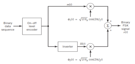
Fig.: BFSK generation(ii) Detection
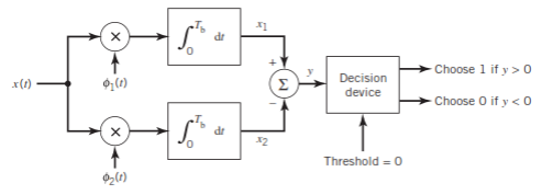
Fig.: BFSK detectionIt consists of two correlators with a common input, and reference signals Ø1(t), Ø2(t) are applied.Then y = x1 – x2The output y is compared with the threshold =0 If y>0 then output = 1 else 0.But if y=0 then the receiver makes a random guess of 0 or 1. Q5) Explain MSK.A5)Minimum Shift Key Modulation is another type of digital modulation technique used to convert a digital signal into analog signals. It is also called Minimum-shift keying (MSK) or Advance Frequency Shift Keying because it is a type of continuous-phase frequency-shift keying.
|
|
|
|
|
(i) Generation
On-off level encoder:Here, the output is of constant amplitude √Eb for input 1 and 0 for input 0.Pair of oscillators: Frequency f1 and f2 differ by integer multiple of 1/Tb. The lower oscillator has frequency f2 preceded by inverter. When in a signal interval, the input symbol is 1, the upper oscillator is switched on, and signal s1(t) is transmitted, while lower oscillator is switched off.When input is 0, upper oscillator is off, lower oscillator is on and signal s2(t) is transmitted.
|
|
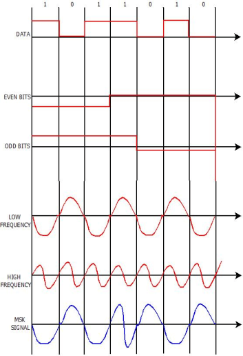
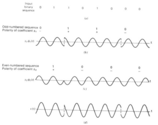
Key features It is encoded with bits alternating between quadrature components, with the Q component delayed by half the symbol period. Minimum Shift Keying is the most effective digital modulation technique. It can be implemented for almost every stream of bits much easier than the Phase Shift Key, Frequency Shift Key and Amplitude Shift Key of digital modulation technique. The Minimum Shift Keying's concept is based on the positioning of bits such as even bits and odd bits for the given bitstream and the bit positioning frequency generating table. MSK is the most widely used digital modulation technology because of its ability and flexibility to handle "One(1)" and "Zero(0)" transition of binary bits.
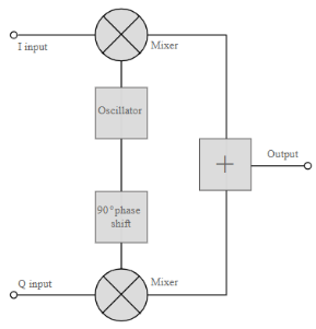
Fig.: MSK output Q6) Explain M-ary QAM in detail.A6)The QAM modulator essentially follows the idea that can be seen from the basic QAM theory where there are two carrier signals with a phase shift of 90° between them. These are then amplitude modulated with the two data streams known as the I or In-phase and the Q or quadrature data streams. These are generated in the baseband processing area.Basic QAM I-Q modulator circuitThe two resultant signals are summed and then processed as required in the RF signal chain, typically converting them in frequency to the required final frequency and amplifying them as required.
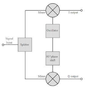
Fig.: Basic QAM It is worth noting that as the amplitude of the signal varies any RF amplifiers must be linear to preserve the integrity of the signal. Any non-linearities will alter the relative levels of the signals and alter the phase difference, thereby distorting he signal and introducing the possibility of data errors.Basic QAM I-Q demodulator circuitThe basic modulator assumes that the two quadrature signals remain exactly in quadrature.A further requirement is to derive a local oscillator signal for the demodulation that is exactly on the required frequency for the signal. Any frequency offset will be a change in the phase of the local oscillator signal with respect to the two double sideband suppressed carrier constituents of the overall signal.Systems include circuitry for carrier recovery that often utilises a phase locked loop - some even have an inner and outer loop. Recovering the phase of the carrier is important otherwise the bit error rate for the data will be compromised.
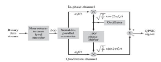
Fig.: Basic QAM demodulator The circuits shown above show the generic IQ QAM modulator and demodulator circuits that are used in a vast number of different areas. Not only are these circuits made from discrete components, but more commonly they are used within integrated circuits that are able to provide a large number of functions. Q7) Explain generation and coherent detection of qpsk signals.A7) (i) GenerationThe QPSK Modulator uses a bit-splitter, two multipliers with local oscillator, a 2-bit serial to parallel converter, and a summer circuit.
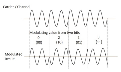
Fig.: QPSK generationAt the modulator’s input, the message signal’s even bits (i.e., 2nd bit, 4th bit, 6th bit, etc.) and odd bits (i.e., 1st bit, 3rd bit, 5th bit, etc.) are separated by the bits splitter and are multiplied with the same carrier to generate odd BPSK (called as PSKI) and even BPSK (called as PSKQ). The PSKQ signal is anyhow phase shifted by 90° before being modulated.The QPSK waveform for two-bits input is as follows, which shows the modulated result for different instances of binary inputs.
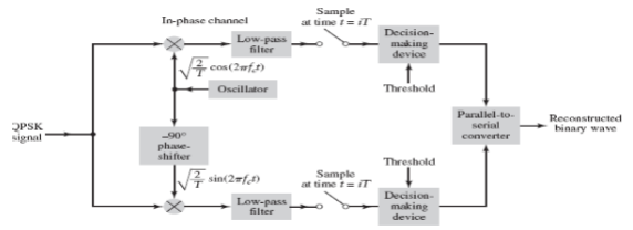
(ii) DetectionThe QPSK Demodulator uses two product demodulator circuits with local oscillator, two band pass filters, two integrator circuits, and a 2-bit parallel to serial converter.
Fig.: QPSK detectorsThe two product detectors at the input of demodulator simultaneously demodulate the two BPSK signals. The pair of bits are recovered here from the original data. These signals after processing are passed to the parallel to serial converter.
Fig.: QPSK output
|
|
|
Fig.: Basic QAM demodulator The circuits shown above show the generic IQ QAM modulator and demodulator circuits that are used in a vast number of different areas. Not only are these circuits made from discrete components, but more commonly they are used within integrated circuits that are able to provide a large number of functions. Q7) Explain generation and coherent detection of qpsk signals.A7) (i) GenerationThe QPSK Modulator uses a bit-splitter, two multipliers with local oscillator, a 2-bit serial to parallel converter, and a summer circuit.
|
|
|
|
0 matching results found
