|
|
|
|
|
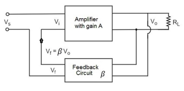
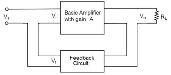
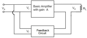
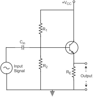
The input signal voltage is applied between base and emitter which develops an output voltage Vo across RE, in the emitter section. Therefore, Vo=IERE ---------------------------(1) The whole of this output current is applied to the input through feedback. Hence, Vf=Vo------------------------------(2) As the output voltage developed across RL is proportional to the emitter current, this emitter follower circuit is a current feedback circuit. Hence, β=VfVo=1----------------------------------(3) The input signal voltage to the transistor (= Vi) is equal to the difference of Vs and Vo i.e., Vi=Vs−Vo---------------------------(4)
|
The Darlington pair is a cascade of two common collector circuits as shown. With input resistance of Q2 acting as Re for Q1.Q1 thus sees a large equivalent Re, but the physical resistance producing this effect is R2 which is much smaller. Emitter of Q1 is at VR2 +VBE2 and is reasonably low voltage, not requiring a high voltage power supply. If IC1=0.1mA Ic2=1mA r2=5K hie=1K and hfe=100 then Re for first stage is 1K+(1+100)5K =506K and VE1 is just 5Kx1mA +0.7 =5.7 V If we had used physical resistance of 500K as Re for first stage and omitted for second stage then Ve1 would have been 500K x 0.1 mA =50V requiring power supply of 100V if Vce=Vre=Vcc/2 . For second stage A12= 1+hfe and R12=(1+fhe) R2 For the first stage load is Ri2 and hoeRi2 is likely to be >0.1 So A11 = (1+hfe)/ (1+hoeR12) = (1+hoe)(1+hfe)R2)=(1+hfe)/(1+hoehfeR2) Overall current gain is A11A12 = (1+hfe) 2 / (1+hoehfeR2) And R1=hie+A12Ri2= (1+hfe)2 R2/ (1+hoehfeR2) R1 for the given parameter is (1+100) 2 x 5K/ (1+25x10-6x100x5K) =50M The Darlington has a drawback that emitter current of first stage is amplified by the current gain of second stage so the first stage drift gets amplified making the circuit drift-prone. The second stage has higher collector current and so the h-parameters of two transistors cannot be considered as same. The effect of bias resistance can be minimised by bootstrapping the CC circuit. Here R1 and R2 are the bias resistances giving base bias through R3. C1 is short circuit the output to point Y at the junction of the bias resistance. Figure. Bootstrap At point X the signal voltage is Vin. Let the signal current in R3 be Ieff . Then Ieff = (Vin-Vout) /R3 So the effective resistance of the combination seen by the source is Reff= Vin/Ieff = Vin R3/ (Vin -Vout) = R3/(1-Av) Where Av = voltage gain Vout/Vin
|
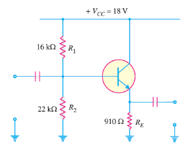
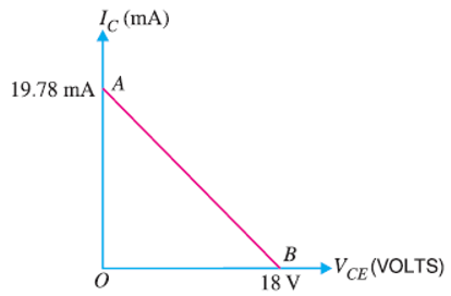
Voltage across R2, V2 = Vcc/R1+R2 xR2 = 18/16+22 x 22 =10.42 V Voltage across RE, VE = V2 – VBE = 10.42 -0.7 = 9.72 V Emitter current IE = VE/RE = 9.72/910 Ω = 10.68mA DC load line Ic(sat) = Vcc/RE = 18/910 = 19.78 mA This locates the point A(OA=19.78mA) of the dc load line VCE (off) =Vcc=18V This locates point B(OB=18V) of the dc load line. By joining points A and B, d.c. load line AB is constructed as shown in figure.
|
