ECD-II
Unit 6 IC Regulators Q 1) What are the features of 78XX?A 1)A positive voltage regulator provides with constant positive output voltage. All those IC’s in the 78XX series are fixed positive voltage regulators. In the IC nomenclature – 78XX ; the part XX denotes the regulated output voltage the IC is designed for. Examples:- 7805, 7806, 7809 etc.Q 2) Explain the schematic of 7805IC?A 2)
Figure 2.Schematic of 7805IC The heart of the 7805 IC is a transistor (Q16) that controls the current between the input and output and thus controlling the output voltage. The bandgap reference (yellow) keeps the voltage stable. It takes the scaled output voltage as input (Q1 and Q6) and provides an error signal (to Q7) for indication if the voltage is too high or low. The key task of the bandgap is to provide a stable and accurate reference, even as the chip’s temperature changes.The error signal from the bandgap reference is amplified by the error amplifier (orange). This amplified signal controls the output transistor through Q15. This closes the negative feedback loop controlling the output voltage.The start-up circuit (green) provides initial current to the bandgap circuit, so it does not get stuck in an “off” state. The circuit in purple provides protection against overheating (Q13), excessive input voltage (Q19) and excessive output current (Q14). These circuits reduce the output current or shutdown the regulator, protecting it from damage in case of a fault. The voltage divider (blue) scales down the voltage on the output pin for use by the bandgap reference.Q 3) Explain the design of 7805IC?A 3)Transformer:Selecting a suitable transformer is of great importance. The current rating and the secondary voltage of the transformer is a crucial factor.The current rating of the transformer depends upon the current required for the load to be driven. The input voltage to the 7805 IC should be at least 2V greater than the required 2V output, therefore it requires an input voltage at least close to 7V. Therefore chose a 6-0-6 transformer with current rating 500mA (Since 6*√2 = 8.4V). Rectifying circuit:The best is using a full wave rectifierIts advantage is DC saturation is less as in both cycle diodes conduct. Higher Transformer Utilization Factor (TUF). 1N4007 diodes are used as its can withstand a higher reverse voltage of 1000v whereas 1N4001 is 50V
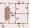
Figure. Center Tap Full Wave RectifierCapacitors:Knowledge of Ripple factor is essential while designing the values of capacitorsIt is given byY=1/(4√3fRC) (as the capacitor filter is used) 1. f= frequency of AC ( 50 Hz)2. R=resistance calculatedR= V/Ic V= secondary voltage of transformer V=6√2=8. 4 R=8.45/500mA=16.9Ω standard 18Ω chosen 3. C=Filtering capacitanceWe have to determine this capacitance for filteringY=Vac-rms/VdcVac-rms = Vr/2√3Vdc= VMax-(Vr/2)Vr= VMax- VMin Vr = 5.2-4.8 =0. 4V Vac-rms = .3464V Vdc = 5V Y=0 .06928 Hence the capacitor value is found out by substituting the ripple factor in Y=1/(4√3fRC)Thus,  and standard 2200µF is chosenUse a 0.01μF capacitor at the output side to avoid transient changes in the voltages due to changes in load and a 0.33μF at the input side of regulator to avoid ripples if the filtering is far away from regulator.Circuit Diagram
Figure-Circuit diagram of 7805IC Q 4) Explain the features of 79XX Voltage regulator?A 4)
Figure. PIN configurationThe pin out configuration of IC 79xx is shown in the diagram above.The pin 1 acts as the Ground terminal (0V). The pin 2 acts as the input terminal (5V to 24V). The pin 3 acts as the output terminal (constant regulated 5V). Q 5) Explain the working of 7912?A 5)IC 79xx is used in circuits as shown in the circuit above. To improve stability, two capacitors—C1 and C2—are used.The capacitor C1 is used only if the regulator is separated from filter capacitor by more than 3". It must be a 2.2 μF solid tantalum capacitor or 25μF aluminium electrolytic capacitor. The capacitor C2 is required for stability. Usually, a 1 μF solid tantalum capacitor is used. 25μF aluminium electrolytic capacitor can also be used. LM7912 IC is used in designing analog circuits which require negative voltages. You can design this IC to get -12 volts. Microcontrollers need a smooth and regulated voltage at the input to function smoothly. Therefore, LM7912 IC is used for generating smooth voltage. It is also useful in designing split power supplies and sensors. Most importantly, it can operate over 0 to 50 °C temperature range. Moreover, it is suitable for use in fixed voltage applications.Q 6) Explain the working of LM317 voltage regulator?A 6)LM 317- Variable Voltage Regulator
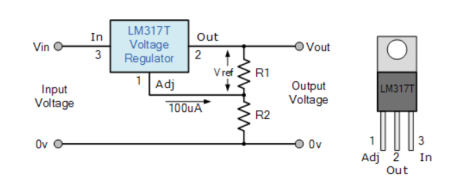
Figure. Variable Voltage Regulator The voltage across the feedback resistor R1 is a constant 1.25V reference voltage, Vref produced between the “output” and “adjustment” terminal. The adjustment terminal current is a constant current of 100uA. Since the reference voltage across resistor R1 is constant, a constant current i will flow through the other resistor R2, resulting in an output voltage of:Vout = 1.25(1+R2/R1)Then whatever current flows through resistor R1 also flows through resistor R2 with the sum of the voltage drops across R1 and R2 being equal to the output voltage,  . Q 7) Explain the design of LM317?A 7)The LM317T has very good load regulation providing that the minimum load current is greater than 10mA. To maintain a constant reference voltage of 1.25V, the minimum value of feedback resistor R1 needs to be 1.25V/10mA = 120 Ohm and this value can range anywhere from 120 ohms to 1,000 ohms with typical values of R1 being about 220Ω’s to 240Ω’s for good stability.If we know the value of the required output voltage, Vout and the feedback resistor R1 is say 240 ohms, then we can calculate the value of resistor R2 from the above equation. For example, our original output voltage of 9V would give a resistive value for R2 of:R1.((Vout/1.25)-1) = 240.((9/1.25)-1) = 1,488 Ohmsor 1,500 Ohms (1k5Ω) to the nearest preferred value. Q 8) Explain the working of LM723 voltage regulator?A 8)
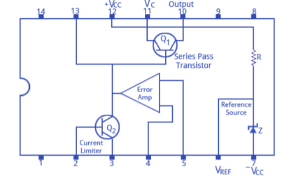
Figure LM 723 Voltage Regulator The functional diagram of the voltage regulator is shown below. It consists of a voltage reference source (Pin 6), an error amplifier with its inverting input on pin 4 and non-inverting input on pin 5, a series pass transistor (pins 10 and 11), and a current limiting transistor on pins 2 and 3. The device can be set to work as both positive and negative voltage regulators with an output voltage ranging from 2 V to 37 V, and output current levels up to 150 m A. The maximum supply voltage is 40 V, and the line and load regulations are each specified as 0.01%. Q 9) Explain the design of LM 723?A 9)Design
Figure. Basic low voltage regulator The resistor, Rsc is connected between CL and CS pins. The current limit transistor remains non-conductive unless drops across Rsc is 0.6 V which is equal to VBE drop. The value of Rsc can be found out by Rsc = Vsense / I limit = 0.6/Ilimit--------------------------------------------------(1)Ilimit can be selected as 1.2 to 1.5 times the maximum load circuit. Potential divider made up of R1 and R2 is connected between Vref and non-inverting terminals.Vnon-inverting = Vref X R2/R1+R2 ------------------------------------------------------(2)As the series pass transistor is working as emitter follower.Vo = Vref x R2/R1+R2 ------------------------------------------------------------------(3)R1 and R2 can be between 1 kΩ to 10 kΩ.R3= R1||R2 R3 = R1R2/R1+R2 ------------------------------------------------------------------------(4)Maximum load current can be 150 mA.Q 10) Explain the applications of voltage regulators?A 10)Voltage regulators find their applications in computers, alternators, power generator plants where the circuit is used to control the output of the plant.
|
|
 and standard 2200µF is chosenUse a 0.01μF capacitor at the output side to avoid transient changes in the voltages due to changes in load and a 0.33μF at the input side of regulator to avoid ripples if the filtering is far away from regulator.Circuit Diagram
|
|
|
 . Q 7) Explain the design of LM317?A 7)The LM317T has very good load regulation providing that the minimum load current is greater than 10mA. To maintain a constant reference voltage of 1.25V, the minimum value of feedback resistor R1 needs to be 1.25V/10mA = 120 Ohm and this value can range anywhere from 120 ohms to 1,000 ohms with typical values of R1 being about 220Ω’s to 240Ω’s for good stability.If we know the value of the required output voltage, Vout and the feedback resistor R1 is say 240 ohms, then we can calculate the value of resistor R2 from the above equation. For example, our original output voltage of 9V would give a resistive value for R2 of:R1.((Vout/1.25)-1) = 240.((9/1.25)-1) = 1,488 Ohmsor 1,500 Ohms (1k5Ω) to the nearest preferred value. Q 8) Explain the working of LM723 voltage regulator?A 8)
|
|
0 matching results found


