LIC
Unit - 1Differential Amplifiers Q1) Two direct-coupled CE amplifiers are placed in series to achieve the desired voltage gain. Design a level shifter to be placed in between the two CE amplifiers to provide a dc voltage sufficiently low to prevent the second CE amplifier from saturating. Do this by providing a 1 V bias to the second stage. The collector voltage, VC, of the first amplifier is 4 V, and the RC of that amplifier is 1 kΩ. Design the level shifter to have an IC of 1 mA using a 10V power supply. Use a current source having β(s) = 100, VBE(s) = 0.7 V, and VON = 0.7 V. A1) We need to find the values of RE, R1, R2, and R’E. Since the first amplifier has a VC of 4 V, the value of VBB is 4 V, whereas the RB of that formula is 1 kΩ. Note this is using the Thevenin equivalent circuit of the previous amplifier.  Setting the current-source transistor operating point in the middle of the dc load line, we have
 and
and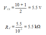 The voltage across R’E is 5.5 V. Then
 We now know the voltages across R1 and R2 and the parallel resistance. This yields two equations, where we assume that the base current in the lower transistor of Figure 9.7(b) is negligible.
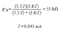 and
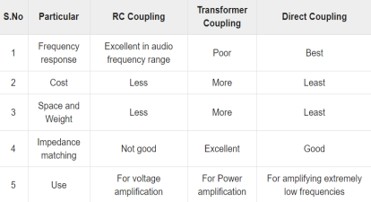
and The design is therefore complete.Q2) Compare the RC coupling, transformer coupling and DC coupling?A2)
  Q3) Explain the need of level shifters?A3) Level shifters are amplifiers that add or subtract a known voltage from the input in order to compensate for dc offset voltages. Op-amps have level shifters included in their design.We begin the analysis by using KVL in the input loop of Figure (a) and letting vin = 0 to obtain
 Now since
 we solve for the dc value of output voltage, Vout.
 Above equation shows that by varying RE, Vout can be set to any desired dc level (limited to a maximum of VBB–VBE). Since VBB is the dc level acquired from the previous stage, this amplifier is used to shift the level downward (to a lower value). If upward shifting is required, a similar circuit is used but pnp transistors are substituted for the npn transistors. A complete circuit with active current source is shown in Figure (b).
 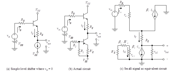 Fig 1 Level Shifter Q4) Explain differential amplifier configuration?A4)
 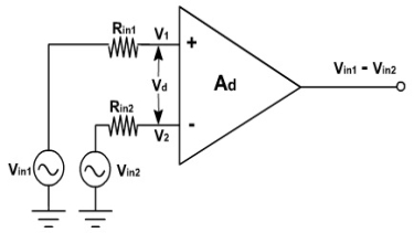 Fig 2 Differential Amplifier
 Vin1 and Vin2 are the two input signals applied at the positive and negative terminals of op-amp. Vout is the desired output voltage whose value is equal to the amplified difference between the input voltages. Op-amp can amplify both ac and dc voltages hence, the input supply voltages can both be ac or dc. Rin1 and Rin2 are source resistances and is negligible w.r.to input resistance Rin. Therefore, the voltage drops across them is also assumed to be zero. Hence the output voltage, Vout= Ad (Vin1 - Vin2)where, Ad is known as open loop gain.Hence the output voltage is directly proportional to the product of voltage gain and difference between input voltages. The polarity of output voltage depends upon polarity of the difference between input voltages. Q5) Explain the current bias circuit?A5) The figure below shows dual input output differential amplifier with constant current bias. The transistor Q3 is used in place of RE. As we have already seen in the dc analysis that for keeping constant IE the value of RE should be very large. This leads to increase in CMRR. TO maintain same value of RE and constant IE current bias is used.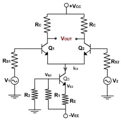 Fig 3 Current Bias Circuit The value of voltage at base of Q3 is given asVB3 =
  (-VEE)VE3 = VB3 – VBE3 =
  (-VEE) – VBE3IBE3 = IC3 =
  Due to symmetry in the differential amplifier IC3 isIE1 = IE2 =
  =
=  The collector current, IC3 in transistor Q3 is fixed because no signal is injected into either the emitter or the base of Q3. Besides supplying constant emitter current, the constant current bias also provides a very high source resistance since the ac equivalent or the dc source is ideally an open circuit. Therefore, all the performance equations obtained for differential amplifier using emitter bias are also valid. As seen in IE expressions, the current depends upon VBE3. If temperature changes, VBE changes and current IE also changes. To improve thermal stability, a diode is placed in series with resistance R1as
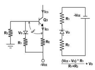 Fig 4 Modified Circuit
 For R1 and R2 are selected such that
 Hence, current IE3 is constant and independent of temperature due to the addition of diode in the circuit. Q6) Explain Current mirror circuit?A6) Here at the Q2 side, more current mirrors need to be used to provide current KID2=KID1. Also, it can be seen that all internal nodes have low impedance except the output node. By using proper current mirrors with high output impedance, good gain can be achieved. The overall transfer function of this Op-Amp closely approximate dominant-pole operation.

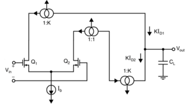 Fig 5 Current mirror circuit If power dissipation is specified, then total current is given by,
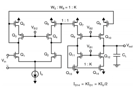 Fig 6 Current mirror using transistor It can be seen that larger K increases the unity-gain frequency assuming the load capacitor dominates the time constants. Larger K also increases the gain. A typical upper limit for K is 5. A detailed analysis reveals important nodes for determining the non-dominant poles, at the drain of Q1 first and drain of Q2 and Q9 secondly. Larger K increases the capacitances at these nodes while also increases the resistance (assuming a fixed Itotal), which reduce the non-dominant poles. In this case, then CL has to be increased to maintain a large phase margin. So, K should not be too large, i.e. K<=2 usually. During slew rate, all of the bias current Ib of the first stage is diverted through Q1/2 and amplified by the current mirror gain to the output. The total current to charge/discharge the load is KIb. So the slew rate is Due primarily to the larger unity-gain frequency and slew rate, the current-mirror Op-Amp may be preferred over the folded-cascade Op-Amp. However, one has to be careful that the current-mirror Op-Amp has larger input noise as well, as its input stage is biased at a lower portion of the total bias current and therefore a relatively smaller gm given the same power consumption. Q7) Explain DC coupling and cascade differential stage?A7) In this type of amplifier, the output of one stage is connected to the input of next stage and hence called as direct coupled amplifier. The circuit is shown below.
 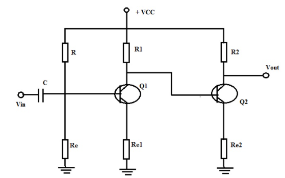 Fig 7 DC Coupled Amplifier There are two transistors Q1 and Q2 with bias resistors R1 and R2 connected across base of Q1 and Q2 respectively. The Q2 is self-biased. The amplifier amplifies ac signal by low frequency. During positive half of input Q1 is forward biased and conducts and provides output at the collector.VCE = VCC-ICRCThis inverted output from stage one is applied as input to base of Q2. The voltage drop across CE is also zero. There are three types of coupling methods are available like RC Coupling, Transformer Coupling, and Direct Coupling. Q8) Explain in detail the AC analysis of dual input balanced output differential amplifier?A8) To perform ac analysis to derive the expression for the voltage gains Ad and input resistance Ri of a differential amplifier: 1) Set the dc voltages +VCC and –VEE at 0 2) Substitute the small signal T equivalent models for the transistors Figure below shows resulting ac equivalent circuit of the dual input balanced output differential amplifier
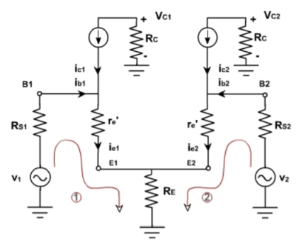 Fig 8 AC equivalent of differential amplifier Voltage Gain: From the circuit above 1) Ie1=Ie2; therefore Re1=Re2. For this reason the ac emitter resistance of transistors Q1 and Q2 is simply denoted by Re . 2) The voltage across each collector resistor is shown out of phase by 1800 w.r.t the input voltages Vin1 and Vin2. Applying Kirchhoff’s voltage law for loops 1 and 2, we get vin1 – Rin1ib1 – re ie1 – RE(ie1+ie2) = 0 ………………………..(5) vin2 – Rin2ie2 – re ie2 – RE(ie1+ie2) = 0 ……………………………(6) Substituting current relations ib1 = ie1/B ac and ib2 = ie2/B ac yields vin1 – Rin1ie1/Bac – re ie1 – RE(ie1+ie2) = 0 vin2 – Rin2ie2/Bac – re ie2 – RE(ie1+ie2) = 0 Generally, Rin1/B ac and Rin2/B ac values are very small therefore we shall neglect them here for simplicity and rearrange these equations as follows: (re+RE)ie1 + RE2ie2 = vin1 ………………………………….(7) RE2ie1 + (re+RE)ie2 = vin2 ……………………………….(8) Eqns (7) and (8) can be solved simultaneously for ie1 and ie2 by using Cramer’s rule: Ie1 = |(vin1/vin2)(RE/re+RE)|/|{(re+RE)/RE}{RE/(re+RE)}| ……………..(9a) ={(re+RE)vin1 – REvin2}/{(re+RE) 2 – (RE)2 } Similarly Ie2 = |(vin1/vin2){(re+RE)/RE}|/|{(re+RE)/RE}{RE/(re+RE)}| …………………….(9b) ={(re+RE)vin2 – REvin2}/{(re+RE) 2 – (RE) 2 } The output voltage is vo = vc2 – vc1 = -RCic2 – (-RCic1) ……………………………(10) = RCic1 – RCic2 =RC(ie1 – ie2) since ic = ie Thus, a differential amplifier amplifies the difference between two input signals as expected, the figure below shows the input and output waveforms of the dual-input balanced-output differential amplifier. By defining vid = vin1 as the difference in input voltages, we can write the voltage-gain equation of the dual-input balanced-output differential amplifier as follows: Ad = vo/vid = RC/re Q9) Explain in detail the DC analysis of dual input balanced output differential amplifier?A9) To determine the operating point values (ICQ and VCEQ) for the differential amplifier, we need to obtain a dc equivalent circuit. The dc equivalent circuit can be obtained simply by reducing the input signals Vin1 and Vin2 to zero. The dc equivalent circuit thus obtained is shown in fig below. Note that the internal resistances of the input signals are denoted by Rin because Rin1 = Rin2.Since both emitter biased sections of the differential amplifier are symmetrical (matched in all respects), we need to determine the operating point collector current ICQ and collector to emitter voltage VCEQ for only one section. We shall determine the ICQ and VCEQ values for transistor Q1 only. These ICQ and VCEQ values can then be used for transistor Q2 also.
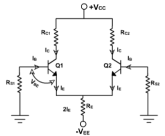 Fig 9 Simplified Differential amplifier Applying Kirchhoff’s voltage law to the base-emitter loop of the transistor Q1, RinIB- VBE - RE(2IE)+VEE = 0…………… (1) But IB = IE/Bdc since IC = IE Thus the emitter current through Q1 is determined directly from eqn(1) as follows : IE = (VEE - VBE)/(2RE + Rin/Bdc) ………………(2) where VBE = 0.6V for silicon transistors VBE =0.2V for germanium transistors Generally, Rin/Bdc<< 2RE.Therefore, eqn(2) can be rewritten as ICQ=IE = (VEE - VBE)/2RE …………………… (3) From eqn (3) we see that the value of RE sets up the emitter current in transistors Q1 and Q2 for a given value of VEE. In other words, by selecting a proper value of RE, we can obtain a desired value of emitter current for a known value of –VEE. Notice that the emitter current in transistors Q1 and Q2 is independent of collector resistance RC. Next we shall determine the collector to emitter voltage VCE. The voltage at the emitter of transistor Q1 is approximately equal to VBE if we assume the voltage drop across Rin to be negligible. Knowing the value of emitter current IE(=IC),we can obtain the voltage at the collector VCC as follows: VC = VCC – RCIC Thus the collector to emitter voltage VCE is VCE = VC - VE = (VCC – RCIC) – (-VEE) VCEQ=VCE = VCC+VBE - RCIC …………………….(4) Thus for both transistors we can determine the operating point values by using the eqns (2)and(4), respectively, because at the operating point IE=ICQ and VCEQ=VCE Remember that the dc analysis eqns (2) and (4) are applicable for all 4 differential amplifier configurations as long as we use the same biasing arrangement for each of them.Q10) Draw the circuit for single input and unbalanced output differential amplifier?A10)
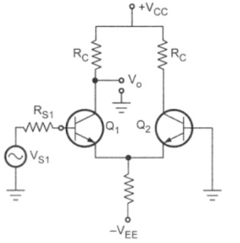 Fig 10 Single input unbalanced outputWhen input signal Vs1 is applied to the transistor Q1, it is amplified and inverted voltage gets generated at the collector of the transistor Q1. At the same time, it is amplified and non-inverted voltage gets generated at the collector of the transistor Q2 as shown in the above diagram. Unbalanced output will contain unnecessary dc content as it is a dc coupled amplifier therefore this configuration should follow by a level translator circuit.
 Setting the current-source transistor operating point in the middle of the dc load line, we have
 and
and The voltage across R’E is 5.5 V. Then
 We now know the voltages across R1 and R2 and the parallel resistance. This yields two equations, where we assume that the base current in the lower transistor of Figure 9.7(b) is negligible.
 and
and The design is therefore complete.Q2) Compare the RC coupling, transformer coupling and DC coupling?A2)
  Q3) Explain the need of level shifters?A3) Level shifters are amplifiers that add or subtract a known voltage from the input in order to compensate for dc offset voltages. Op-amps have level shifters included in their design.We begin the analysis by using KVL in the input loop of Figure (a) and letting vin = 0 to obtain
 Now since
 we solve for the dc value of output voltage, Vout.
 Above equation shows that by varying RE, Vout can be set to any desired dc level (limited to a maximum of VBB–VBE). Since VBB is the dc level acquired from the previous stage, this amplifier is used to shift the level downward (to a lower value). If upward shifting is required, a similar circuit is used but pnp transistors are substituted for the npn transistors. A complete circuit with active current source is shown in Figure (b).
  Fig 1 Level Shifter Q4) Explain differential amplifier configuration?A4)
  Fig 2 Differential Amplifier
  Fig 3 Current Bias Circuit The value of voltage at base of Q3 is given asVB3 =
  (-VEE)VE3 = VB3 – VBE3 =
  (-VEE) – VBE3IBE3 = IC3 =
  Due to symmetry in the differential amplifier IC3 isIE1 = IE2 =
  =
=  The collector current, IC3 in transistor Q3 is fixed because no signal is injected into either the emitter or the base of Q3. Besides supplying constant emitter current, the constant current bias also provides a very high source resistance since the ac equivalent or the dc source is ideally an open circuit. Therefore, all the performance equations obtained for differential amplifier using emitter bias are also valid. As seen in IE expressions, the current depends upon VBE3. If temperature changes, VBE changes and current IE also changes. To improve thermal stability, a diode is placed in series with resistance R1as
 Fig 4 Modified Circuit
 For R1 and R2 are selected such that
 Hence, current IE3 is constant and independent of temperature due to the addition of diode in the circuit. Q6) Explain Current mirror circuit?A6) Here at the Q2 side, more current mirrors need to be used to provide current KID2=KID1. Also, it can be seen that all internal nodes have low impedance except the output node. By using proper current mirrors with high output impedance, good gain can be achieved. The overall transfer function of this Op-Amp closely approximate dominant-pole operation.

 Fig 5 Current mirror circuit If power dissipation is specified, then total current is given by,
 Fig 6 Current mirror using transistor It can be seen that larger K increases the unity-gain frequency assuming the load capacitor dominates the time constants. Larger K also increases the gain. A typical upper limit for K is 5. A detailed analysis reveals important nodes for determining the non-dominant poles, at the drain of Q1 first and drain of Q2 and Q9 secondly. Larger K increases the capacitances at these nodes while also increases the resistance (assuming a fixed Itotal), which reduce the non-dominant poles. In this case, then CL has to be increased to maintain a large phase margin. So, K should not be too large, i.e. K<=2 usually. During slew rate, all of the bias current Ib of the first stage is diverted through Q1/2 and amplified by the current mirror gain to the output. The total current to charge/discharge the load is KIb. So the slew rate is Due primarily to the larger unity-gain frequency and slew rate, the current-mirror Op-Amp may be preferred over the folded-cascade Op-Amp. However, one has to be careful that the current-mirror Op-Amp has larger input noise as well, as its input stage is biased at a lower portion of the total bias current and therefore a relatively smaller gm given the same power consumption. Q7) Explain DC coupling and cascade differential stage?A7) In this type of amplifier, the output of one stage is connected to the input of next stage and hence called as direct coupled amplifier. The circuit is shown below.
  Fig 7 DC Coupled Amplifier There are two transistors Q1 and Q2 with bias resistors R1 and R2 connected across base of Q1 and Q2 respectively. The Q2 is self-biased. The amplifier amplifies ac signal by low frequency. During positive half of input Q1 is forward biased and conducts and provides output at the collector.VCE = VCC-ICRCThis inverted output from stage one is applied as input to base of Q2. The voltage drop across CE is also zero. There are three types of coupling methods are available like RC Coupling, Transformer Coupling, and Direct Coupling. Q8) Explain in detail the AC analysis of dual input balanced output differential amplifier?A8) To perform ac analysis to derive the expression for the voltage gains Ad and input resistance Ri of a differential amplifier: 1) Set the dc voltages +VCC and –VEE at 0 2) Substitute the small signal T equivalent models for the transistors Figure below shows resulting ac equivalent circuit of the dual input balanced output differential amplifier
 Fig 8 AC equivalent of differential amplifier Voltage Gain: From the circuit above 1) Ie1=Ie2; therefore Re1=Re2. For this reason the ac emitter resistance of transistors Q1 and Q2 is simply denoted by Re . 2) The voltage across each collector resistor is shown out of phase by 1800 w.r.t the input voltages Vin1 and Vin2. Applying Kirchhoff’s voltage law for loops 1 and 2, we get vin1 – Rin1ib1 – re ie1 – RE(ie1+ie2) = 0 ………………………..(5) vin2 – Rin2ie2 – re ie2 – RE(ie1+ie2) = 0 ……………………………(6) Substituting current relations ib1 = ie1/B ac and ib2 = ie2/B ac yields vin1 – Rin1ie1/Bac – re ie1 – RE(ie1+ie2) = 0 vin2 – Rin2ie2/Bac – re ie2 – RE(ie1+ie2) = 0 Generally, Rin1/B ac and Rin2/B ac values are very small therefore we shall neglect them here for simplicity and rearrange these equations as follows: (re+RE)ie1 + RE2ie2 = vin1 ………………………………….(7) RE2ie1 + (re+RE)ie2 = vin2 ……………………………….(8) Eqns (7) and (8) can be solved simultaneously for ie1 and ie2 by using Cramer’s rule: Ie1 = |(vin1/vin2)(RE/re+RE)|/|{(re+RE)/RE}{RE/(re+RE)}| ……………..(9a) ={(re+RE)vin1 – REvin2}/{(re+RE) 2 – (RE)2 } Similarly Ie2 = |(vin1/vin2){(re+RE)/RE}|/|{(re+RE)/RE}{RE/(re+RE)}| …………………….(9b) ={(re+RE)vin2 – REvin2}/{(re+RE) 2 – (RE) 2 } The output voltage is vo = vc2 – vc1 = -RCic2 – (-RCic1) ……………………………(10) = RCic1 – RCic2 =RC(ie1 – ie2) since ic = ie Thus, a differential amplifier amplifies the difference between two input signals as expected, the figure below shows the input and output waveforms of the dual-input balanced-output differential amplifier. By defining vid = vin1 as the difference in input voltages, we can write the voltage-gain equation of the dual-input balanced-output differential amplifier as follows: Ad = vo/vid = RC/re Q9) Explain in detail the DC analysis of dual input balanced output differential amplifier?A9) To determine the operating point values (ICQ and VCEQ) for the differential amplifier, we need to obtain a dc equivalent circuit. The dc equivalent circuit can be obtained simply by reducing the input signals Vin1 and Vin2 to zero. The dc equivalent circuit thus obtained is shown in fig below. Note that the internal resistances of the input signals are denoted by Rin because Rin1 = Rin2.Since both emitter biased sections of the differential amplifier are symmetrical (matched in all respects), we need to determine the operating point collector current ICQ and collector to emitter voltage VCEQ for only one section. We shall determine the ICQ and VCEQ values for transistor Q1 only. These ICQ and VCEQ values can then be used for transistor Q2 also.
 Fig 9 Simplified Differential amplifier Applying Kirchhoff’s voltage law to the base-emitter loop of the transistor Q1, RinIB- VBE - RE(2IE)+VEE = 0…………… (1) But IB = IE/Bdc since IC = IE Thus the emitter current through Q1 is determined directly from eqn(1) as follows : IE = (VEE - VBE)/(2RE + Rin/Bdc) ………………(2) where VBE = 0.6V for silicon transistors VBE =0.2V for germanium transistors Generally, Rin/Bdc<< 2RE.Therefore, eqn(2) can be rewritten as ICQ=IE = (VEE - VBE)/2RE …………………… (3) From eqn (3) we see that the value of RE sets up the emitter current in transistors Q1 and Q2 for a given value of VEE. In other words, by selecting a proper value of RE, we can obtain a desired value of emitter current for a known value of –VEE. Notice that the emitter current in transistors Q1 and Q2 is independent of collector resistance RC. Next we shall determine the collector to emitter voltage VCE. The voltage at the emitter of transistor Q1 is approximately equal to VBE if we assume the voltage drop across Rin to be negligible. Knowing the value of emitter current IE(=IC),we can obtain the voltage at the collector VCC as follows: VC = VCC – RCIC Thus the collector to emitter voltage VCE is VCE = VC - VE = (VCC – RCIC) – (-VEE) VCEQ=VCE = VCC+VBE - RCIC …………………….(4) Thus for both transistors we can determine the operating point values by using the eqns (2)and(4), respectively, because at the operating point IE=ICQ and VCEQ=VCE Remember that the dc analysis eqns (2) and (4) are applicable for all 4 differential amplifier configurations as long as we use the same biasing arrangement for each of them.Q10) Draw the circuit for single input and unbalanced output differential amplifier?A10)
 Fig 10 Single input unbalanced outputWhen input signal Vs1 is applied to the transistor Q1, it is amplified and inverted voltage gets generated at the collector of the transistor Q1. At the same time, it is amplified and non-inverted voltage gets generated at the collector of the transistor Q2 as shown in the above diagram. Unbalanced output will contain unnecessary dc content as it is a dc coupled amplifier therefore this configuration should follow by a level translator circuit.
 0 matching results found