|
 =
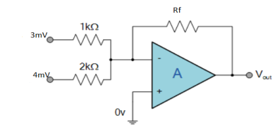
=  Hence, Av1 =
  Av2 =
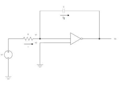
Av2 =  Now, Output voltage Vo = Sum of the two amplified input signalsVo = Av1 x V1 + Av2 x V2Vo =(-5 x 3) + ( -2.5x 4) mVVo = -25mVAs the above output voltage is negative hence it is an inverting amplifier. Q3) The integrator circuit as shown in the figure has R = 500K Ω and C=1µF. Find and plot the output voltage for the inputs as shown in the figure.
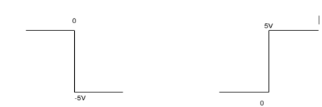
a) b) c)vi= 2 sin 4tV d) vi= 4tV
|
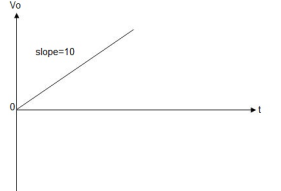
We know that v0 = - 1/RC Here R= 500K Ω and C = 1µF 1/RC = 1/ 500 x 1000 x 1 x 10-6 = 1/RC = 2 = -2 = -2 = 10t V Which means it is a ramp voltage with positive slope.
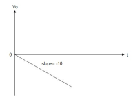
When vi=5V -2 = -2 = -10t V Which means it is a ramp voltage with negative slope.
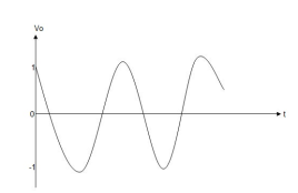
When vi= 2 sin4t V Vo = -2 = -4 [-cos 4t] /4 = cos 4t
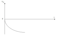
When vi=4t V
Vo =
= -8 [t2/2] = - 4V
|
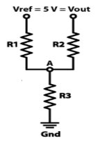
A4)
Vout = 0V
Va = 166V Vout = 5V
Va = 333V
|
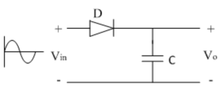
A5) Rectifier circuit gives average value of input signal; but in practice we need peak value of input signal. This is achieved by peak detector circuit. The following figure shows a simple peak detector circuit using diode and capacitor.
Fig 1 Peak detector In the positive half cycle, diode D is forward biased and capacitor C starts charging. When input reaches its peak value, capacitor gets charged to positive peak value.
But in practice, output is taken across some load RL, so when input voltage decreases capacitor discharges through load RL. To avoid this, select RL of very large value so that capacitor discharges very slowly hence almost hold the charge. Whatever charge it lost through RL is gets back in next half cycle.
|
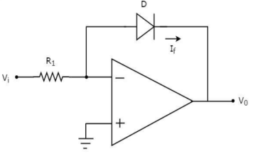
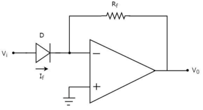
A6) As the name says it is an amplifier which produces the output proportional to logarithmic of the applied input. The log amplifier using op-amp is shown below. The input is applied through the inverting end of op-amp. As the non-inverting end has voltage zero then by virtual ground concept the voltage at inverting terminal also becomes zero.
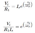
Fig 2 Log Amplifier The equation for input voltage will be
If = The current flowing through diode is given as
Where: Is = Saturation Current Vf = Voltage drop across diode in forward bias VT = Thermal equivalent voltage For feedback loop the KVL equation will be 0-Vf -V0 = 0 Vf = -V0 Substituting Vf in above equation of If
Equating both equations of If
Taking natural log of both sides we get
The above equations shows that the output is natural log of the applied input.
|
A7) This device produces the output proportional to antilog of input. The inverting op-amp is used in this case as well. The figure below shows an antilog amplifier with its inverting terminal connected to the input end with diode and the non-inverting terminal is grounded.
Fig 3 Antilog Amplifier Applying KCL at input terminal we get
The current flowing through diode is given as
Substituting If in above voltage equation we get
At inverting terminal applying KVL we get
Substituting Vf in equation of V0 we get
The above equations shows that the output is natural antilog of the applied input.
|
|
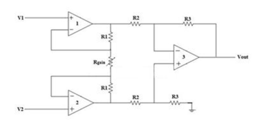
A9) The Instrumentation amplifiers consist of three op-amps. In this circuit, a non-inverting amplifier is connected to each input of the differential amplifier. This instrumentation amplifier provides high input impedance for exact measurement of input data from transducers. The circuit diagram of an instrumentation amplifier is as shown in the figure below.
Fig 3 Instrumentation Amplifier The op-amps 1 & 2 are non-inverting amplifiers and together form an input stage of the instrumentation amplifier. The op-amp 3 is a difference amplifier that forms the output stage of the instrumentation amplifier. Working The output stage of the instrumentation amplifier is a difference amplifier, whose output Vout is the amplified difference of the input signals applied to its input terminals. If the outputs of op-amp 1 and op-amp 2 are Vo1 and Vo2 respectively, then the output of the difference amplifier is given by, Vout = (R3/R2)(Vo1-Vo2) The expressions for Vo1 and Vo2 can be found in terms of the input voltages and resistances. Consider the input stage of the instrumentation amplifier as shown in the figure below.
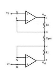
Fig 4 Input Stage of Instrumentation Amplifier The potential at node A is the input voltage V1. Hence the potential at node B is also V1, from the virtual short concept. Thus, the potential at node G is also V1. The potential at node D is the input voltage V2. Hence the potential at node C is also V2, from the virtual short. Thus, the potential at node H is also V2. Ideally the current to the input stage op-amps is zero. Therefore, the current I through the resistors R1, Rgain and R1 remains the same. Applying Ohm’s law between the nodes E and F, I = (Vo1-Vo2)/(R1+Rgain+R1) ——————— 1 I = (Vo1-Vo2)/(2R1+Rgain) Since no current is flowing to the input of the op-amps 1 & 2, the current I between the nodes G and H can be given as, I = (VG-VH)/Rgain = (V1-V2)/Rgain ————————- 2 Equating equations 1 and 2, (Vo1-Vo2)/(2R1+Rgain) = (V1-V2)/Rgain (Vo1-Vo2) = (2R1+Rgain)(V1-V2)/Rgain —————— 3 The output of the difference amplifier is given as, Vout = (R3/R2) (Vo1-Vo2) Therefore, (Vo1 – Vo2) = (R2/R3)Vout Substituting (Vo1 – Vo2) value in the equation 3, we get (R2/R3)Vout = (2R1+Rgain)(V1-V2)/Rgain i.e. Vout = (R3/R2){(2R1+Rgain)/Rgain}(V1-V2) The above equation gives the output voltage of an instrumentation amplifier. The overall gain of the amplifier is given by the term (R3/R2){(2R1+Rgain)/Rgain}.
|
