|
|
|
|
|
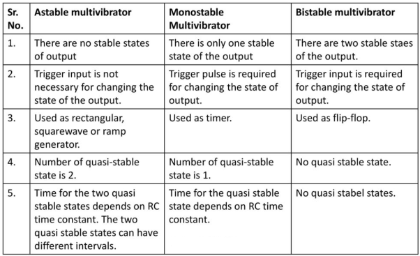
A4) This means there will be no stable level at the output. So, the output will be swinging between high and low. This character of unstable output is used as a clock or square wave output for many applications.
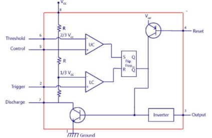
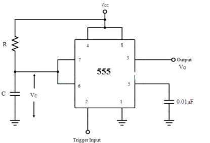
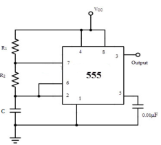
Fig 5 Astable Multivibrator It is self-triggered multivibrator as pin 2 and 6 are connected. The supply is given through pin 8 and the output is obtained through pin 3. The timer will be reset if a low signal is given to pin 4. The capacitor is connected across pin 5 so that the external noise or any dc level are filtered. The resistor pair R1 and R2 form a circuit for determining the width of the output pulse.
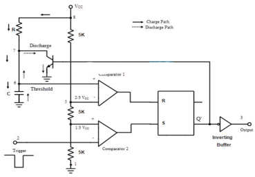
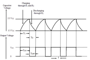
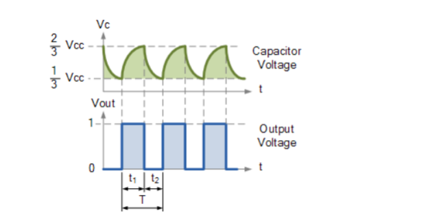
Fig 6 Capacitor and Output voltage waveform During charging the capacitor charges through R1 and R2 and voltage across capacitor rises exponentially and during discharging the capacitor discharges through R2 and voltage falls exponentially. The output is obtained across pin 3. The time for which capacitor charges from 1/3VCC to 2/3VCC is equal to the time the output is high which is given by tc= 0.69(R1+R2) C The discharging time from 2/3Vcc to 1/3VCC is given as td= 0.69 R2C The total period of output waveform is given by T = tc+ td = 0.69(R1+2R2) C The frequency of oscillations is given by f0 = The duty cycle is defined as the ratio of the charging time of capacitor at which the output is high to the total time period. %duty cycle = |
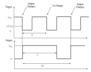
A5) In bi-stable mode, both the output states are stable. At each interrupt, the output changes from low (0) to high (1) and vice versa and stays there. For example, if we have a high (1) output, it will go low(0) once it receives an interrupt and stays low (0) till the next interrupt changes the status.
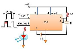
Fig7 Bistable Multivibrator using 555 timer and the output waveform
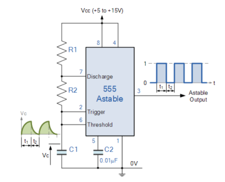
In the 555 Oscillator circuit above, pin 2 and pin 6 are connected allowing the circuit to re-trigger itself on each and every cycle allowing it to operate as a free running oscillator. During each cycle capacitor, C charges up through both timing resistors, R1 and R2 but discharges itself only through resistor, R2 as the other side of R2 is connected to the discharge terminal, pin 7. Then the capacitor charges up to 2/3Vcc which is determined by 0.693(R1+R2)C combination and discharges itself down to 1/3Vcc (the lower comparator limit) determined by the 0.693(R2*C) combination. This results in an output waveform whose voltage level is approximately equal to Vcc – 1.5V and whose output “ON” and “OFF” time periods are determined by the capacitor and resistors combinations. The individual times required to complete one charge and discharge cycle of the output is therefore given as: t 1 = 0.693 (R1 + R2). C and t 2 = 0.693 x R2 x C where, R is in Ω and C in Farads. T = t1 + t2 = 0.693 (R1 + 2 R2) . C f = 1/T = 1.44/ (R1 + 2 R2) . C Duty Cycle = TON / TOFF + TON = R1 + R2 / (R1 + 2R2) %
|
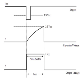
A6) Frequency Divider The monostable multivibrator can be used as frequency divider by adjusting the time interval off charging. The charging time is made larger than the period of input pulse the device acts as divide-by-2 network. By proper selection of R and C the timing interval can be controlled. The waveform is shown below.
Fig 8 Divide-by-2 circuit waveform When negative input pulse is applied the output goes high and will remain high irrespective of any other input pulse application as the timing interval s greater than the time period of trigger pulse. The circuit is triggered for every alternate negative going pulse. Pulse Stretcher This application makes use of the fact that output pulse width of monostable multivibrator is larger than the negative pulse width of trigger pulse. The output of monostable multivibrator is the stretched form of the input pulse. The pulse stretcher is shown below.
Fig 9 Pulse Stretcher
|
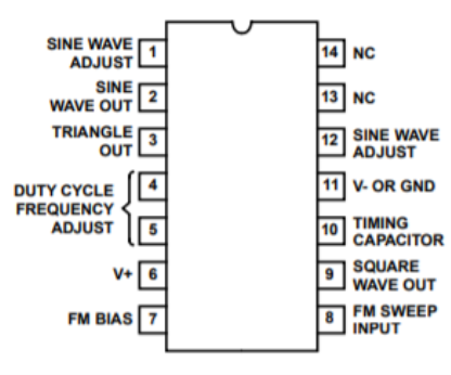
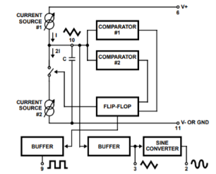
A7) It is a monolithic IC which can produce various waveforms such as sine, square, triangular, sawtooth, pulse with high accuracy. The pin diagram and functional diagram are shown below. [ref. Harris semiconductor]
Fig 10 Pin Diagram of IC 8038
Fig 11 Block diagram of IC 8038
It is a 14 pin PDIP chip. The sine wave is obtained through pin 2. The triangular wave through pin 3. The supply is given through pin 6. An external capacitor C is charged and discharged by two current sources. Current source #2 is switched on and off by a flip-flop, while current source #1 is on continuously. Assuming that the flip-flop is in a state such that current source #2 is off, and the capacitor is charged with a current I, the voltage across the capacitor rises linearly with time. When this voltage reaches the level of comparator #1 (set at 2/3 of the supply voltage), the flip-flop is triggered, changes states, and releases current source #2. This current source normally carries a current 2I, thus the capacitor is discharged with a net-current I and the voltage across it drops linearly with time. When it has reached the level of comparator #2 (set at 1/3 of the supply voltage), the flip-flop is triggered into its original state and the cycle starts again. With the current sources set at I and 2I respectively, the charge and discharge times are equal. Thus, a triangle waveform is created across the capacitor and the flip-flop produces a square wave. The sine wave is created by feeding the triangle wave into a nonlinear network. This network provides a decreasing shunt impedance as the potential of the triangle moves toward the two extremes.
|
A8) t1 – capacitor charge “ON” time is calculated as: t1 = 0.693(R1 + R2). C = 0.693(1000 +2000) x 10 x 10 -6 = 0.021 s= 0.21 msec t2 – capacitor discharge “OFF” time is calculated as: t2 = 0.693 R2. C = 0.693 X 2000 x 10 x 10 -6 = 14ms
Total periodic time (T) is therefore calculated as: T = t1 + t2 = 21 ms + 14 ms = 35 ms. The output frequency, ƒ is therefore given as: f = 1/T = 1/35ms = 28.6 Hz Giving a duty cycle value of: Duty Cycle = R1 + R2 / (R1 + 2 R2) = 1000 + 2000/ (1000 + 2 x 2000) = 60%
|
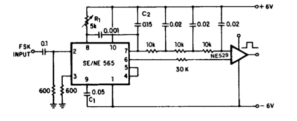
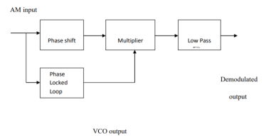
Fig 12 IC 565 PLL A PLL may be used to demodulate AM signals as shown in the figure below. The PLL is locked to the carrier frequency of the incoming AM signal. The output of VCO which has the same frequency as the carrier, but unmodulated is fed to the multiplier. Since VCO output is always 900 before being fed to the multiplier. This makes both the signals applied to the multiplier and the difference signals, the demodulated output is obtained after filtering high frequency components by the LPF. Since the PLL responds only to the carrier frequencies which are very close to the VCO output, a PLL AM detector exhibits high degree of selectivity and noise immunity which is not possible with conventional peak detector type AM modulators.
Fig 13 AM Demodulation
FM Demodulation: If PLL is locked to a FM signal, the VCO tracks the instantaneous frequency of the input signal. The filtered error voltage which controls the VCO and maintains lock with the input signal is the demodulated FM output. The VCO transfer characteristics determine the linearity of the demodulated output. Since, VCO used in IC PLL is highly linear, it is possible to realize highly linear FM demodulators.
|
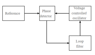
A10) A basic phase locked loop, PLL, consists of three basic elements:
Fig 14 Block Diagram of PLL
|
