Unit 1
MOS Devices
Q1)Explain the MOS transistor?
A1) The diagram showing a typical MOSFET
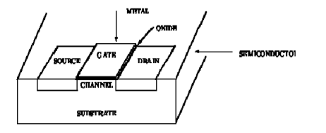
Figure1. MOS Transistor
The transistor consists of three regions, labelled as the source'', the gate'' and the drain''. The area labelled as the gate region is actually a sandwich'' consisting of the underlying substrate material, which is a single crystal of semiconductor material usually silicon; a thin insulating layer usually silicon dioxide; and an upper metal layer. Electrical charge, or current, can flow from the source to the drain depending on the charge applied to the gate region. The semiconductor material in the source and drain region are doped'' with a different type of material than in the region under the gate, so an NPN or PNP type structure exists between the source and drain region of a MOSFET.
Q2)Explain the V-I characteristics of NMOS?
A2) An n-channel enhancement type MOSFET with vGS and vDS applied. The normal directions of current flow are indicated.
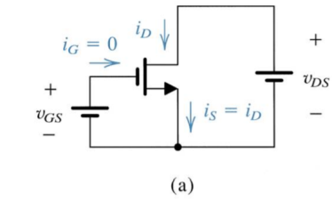
Figure 2. N-channel enhancement type MOSFET
The i-v characteristics comprise a family of curves.
• Each curve corresponds to different value of VGS.
The ID - VDS characteristics for a device with Vt = 1 V and kn(W/L) = 0.5 mA/V2.
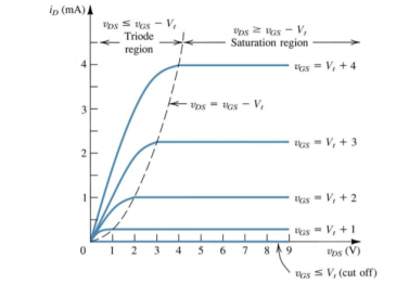
Figure 3. V-I characteristics of NMOS
Three distinct regions of operation can be clearly seen:
Cutoff region:
vGS ≤ Vt no channel induced --------------------------------------(1)
iD = 0-----------------------------------------------------------------------------(2)
Triode region: vGS > Vt channel induced -----------------------------------(3)
vDS ≤ vGS − Vt continuous channel -----------------------------------------------------(4)
iD = k n’ W/ L [(vGS − Vt)vDS – 1/ 2 v2 DS -----------------------------------------------(5)
Saturation region:
vGS > Vt channel induced -------------------(6)
vDS ≥ vGS − Vt pinched − off channel ---------------------(7)
iD = 1/ 2 k n ‘(W/ L) (vGS − Vt) 2 -----------------------------------------------(8)
Boundary between triode and saturation regions: vDS = vGS − Vt.
In saturation current is independent of vds and increases as the square of vgs. This is termed as square law behaviour. In saturation MOSFET is an ideal current source. The current does not depend on vds.
Q4)Explain the V-I characteristics of PMOS?
A4) Figure 5 shows the transfer characteristics of p-type enhancement MOSFETs from which it is evident that IDS remains zero (cutoff state) untill VGS becomes equal to -VT. This is because, only then the channel will be formed to connect the drain terminal of the device with its source terminal. After this, the IDS is seen to increase in reverse direction with the decrease in the value of VDS. This means that the device is functioning in its ohmic region wherein the current through the device increases with an increase in the applied voltage (which will be VSD).
However as VDS becomes equal to –VP, the device enters into saturation during which a saturated amount of current (IDSS) flows through the device, as decided by the value of VGS.
Further it is to be noted that the value of saturation current flowing through the device is seen to increase as the VGS becomes more and more negative i.e. saturation current for VGS3 is greater than that for VGS2 and that in the case of VGS4 is much greater than both of them as VGS3 is more negative than VGS2 while VGS4 is much more negative when compared to either of them (Figure 2b). In addition, from the locus of the pinch-off voltage it is also clear that as VGS becomes more and more negative, even the negativity of VP also increases.
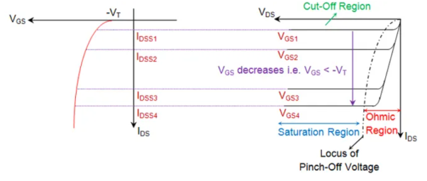
Figure 5. Transfer and Output characteristics
Q5) Explain the transfer characteristics of CMOS Inverter?
A5)Consider the schematic diagram of inverter.
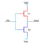
Figure 6. CMOS Inverter
CMOS inverter consists of two transistors a pull-up pMOS transistor(T1) and a pull-down nMOS transistor(T2). When the input voltage Vin is equal to Vdd we get an output voltage of Vss mostly equal to 0 and vice versa. Since it inverts the logic level of input this circuit is called an inverter.
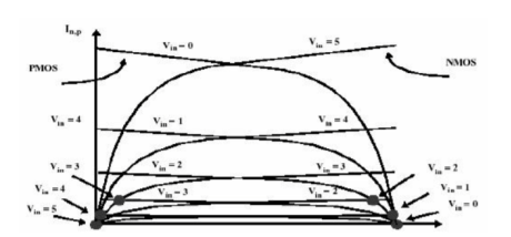
Figure 7.I-V characteristics
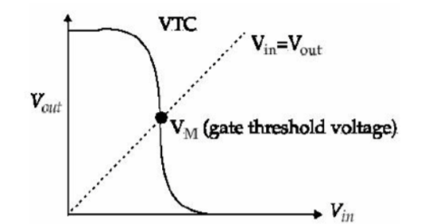
Figure 8.Transfer characteristics
The I-V characteristics of the p-device is reflected about x-axis. This step is followed by taking the absolute values of the pdevice, Vds and superimposing the two characteristics. Solving Vinn and Vinp and Idsn=Idsp gives the desired transfer characteristics of a CMOS inverter as in fig7.
Q6) Explain the detailed analysis of CMOS Inverter?
A6)
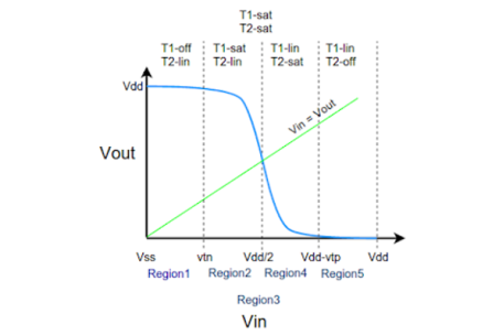
Figure 9. Voltage transfer characteristics
The VTC is divided into five regions(1-5) . The above shown curve is possible when both T1 and T2 are matched for optimum operation. Optimum operation is achieved when Vin = Vdd/2 and we get Vout = Vdd/2 . This is achieved by adjusting width and length of both T1 and T2 as other parameters like mobility, oxide capacitance vary between different technologies.
Consider the following table:
Device | Cutoff | Linear | Saturated |
NMOS | 1. Vgsn < Vtn
| 1. Vgsn > Vtn 2. Vdsn < Vgsn - Vtn | 1. Vgsn > Vtn 2. Vdsn > Vgsn - Vtn |
PMOS | 1. Vgsp > Vtp | 1. Vgsp < Vtp 2. Vdsp > Vgsp - Vtp | 1. Vgsp < Vtp 2. Vdsp < Vgsp - Vtp |
Region-1
In this region the input is in the range of (0,Vtn). Since the input voltage is less than Vtn, the NMOS is in cutoff region. No current flows from Vdd to Vss, The entire Vdd will appear at the Output terminal.
Region-2
In this region the input is in the range of (Vtn,Vdd/2). Since the input voltage is greater than Vtn the NMOS is conducting and it jumps to saturation as it has large Vds across it(Vout is high). PMOS still remains in the linear region.
Region-3
In this region the input voltage is Vdd/2. At this point the output voltage is also Vdd/2 as in figure-2. At this voltage both the NMOS and PMOS are in saturation and the output drops drastically from Vdd to Vdd/2. At this point a large amount of current flows from the supply. Most of the power consumed in CMOS inverter is at this point. Care should be taken that the Input should not stay at Vdd/2 for more amount of time.
Region-4
In this region the input voltage is in the range of (Vdd/2 , Vdd-Vtp). Here the PMOS remains in saturation as Vout < Vin - Vtp and Vgsp < Vtp. But the NMOS moves from saturation to linear region since the drain to source voltage now is less than Vgsn-Vtn.
Region-5
In this region the input voltage is in the range of (Vdd-Vtp,Vdd). Here the PMOS moves from saturation to cutoff as the Vgsp is so high that Vgsp > Vtp. The NMOS still remains in linear as the drain to source voltage now is less than Vgsn-Vtn.
Q7) Realize NOR gate ?
A7) The CMOS implementation of a NOR gate (F = A + B) is shown in Figure. The output of this network is high, if and only if both inputs A and B are low. The worst-case pull-down transition happens when only one of the NMOS devices turns on (i.e., if either A or B is high).
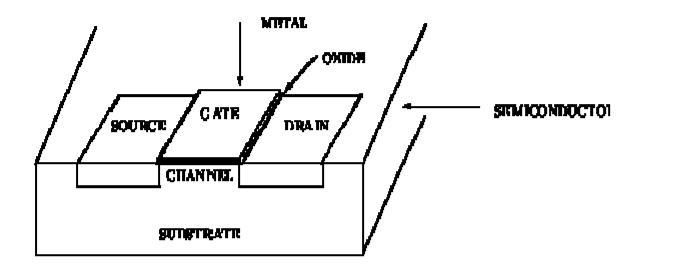
Fig 10. Sizing of a NOR gate to produce the same delay as an inverter with size of NMOS:
Q8) What is parasitic capacitive effect?
A8) When two conductive elements on a PCBA are close to each other and at different voltage levels they form an intrinsic and typically unwanted capacitor. This is known as the parasitic capacitive effect.
Q9) What are its effects of parasitic capacitance?
A9)
Q10) What are its effects at low and high frequencies?
A10) At low frequencies, the effects of parasitic capacitance are minimal. However, at high frequencies, they can be quite significant. Another problem area is when the component is an amplifier as the capacitance between input and output can form a feedback path and generate high-frequency oscillations.
Q11) What are the advantages of CMOS inverter?
A11) The CMOS inverter has two important advantages over the other inverter configurations. The first and perhaps the most important advantage is that the steady-state power dissipation of the CMOS inverter circuit is virtually negligible, except for small power dissipation due to leakage currents.