Unit 2
CMOS IC Fabrication and Layout
Q1) What is CMOS technology?
A1) CMOS technology is a prevailing technology for manufacturing integrated circuits. CMOS stands for “Complementary Metal Oxide Semiconductor”. Microprocessors, batteries, and digital sensors among other electronic components make use of this technology due to several key advantages. This technology uses both NMOS and PMOS to realize various logic functions. Both N and P MOSFET channels are designed for matching characteristics.
Q2)Explain self -aligned CMOS process?
A2) The gate mask works as a mask for n+/p+ diffusion mask, and there’s no need for separate gate mask and diffusion masks, the diffusion masks are only used to differentiate between n+ diffusion and p+ diffusion areas or we can use a single mask for n+ diffusion and complement it to define p+ diffusion.
In step (g) we have defined the gate area by growing polysilicon at their respective locations defined by the gate mask. The polysilicon gate now enables us to diffuse the n+ and p+ regions without the need for growing SiO2 and applying a new mask to define source and drain regions of the MOS (n+ diffuse regions).
In step (h) the wafer will be diffused with n+ using polysilicon gate as an alignment mask. That is the polysilicon aligns the source and the drain to be exactly under the gate.
This approach solves the problem of random misalignment errors, which caused the speed of the device to be dramatically influenced by it.
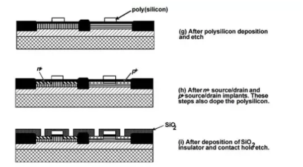
Figure 1. Self aligned CMOS process
Q3) What are the advantages of self aligned CMOS process?
A3) The importance of self-aligned gates comes in the process used to make them. The process of using the gate oxide as a mask for the source and drain diffusion both simplifies the process and greatly improves the yield.
Q4) Explain the Nwell process?
A4) The process starts with a p-substrate.
Step 1 : A thin layer of SiO2 is deposited which will serve as a the pad oxide.
Step 2 : Deposition of a thicker sacrificial silicon nitride layer by chemical vapour deposition (CVD).
Step 3 : A plasma etching process using the complementary of the active area mask to create trenches used for insulating the devices.
Step 4 : The trenches are filled with SiO2 which is called as the field oxide.
Step 5 : To provide flat surface chemical mechanical planerization is performed and also sacrificial nitride is removed.
Step 6 : The n-well mask is used to expose only the n-well areas, after this implant and annealing sequence is applied to adjust the well doping. This is followed by second implant step to adjust the threshold voltage of the PMOS transistor.
Step 7 : Implant step is performed to adjust the threshold voltage of NMOS transistor.
Step 8 : A thin layer of gate oxide and polysilicon is chemically deposited and patterned with the help of polysilicon mask.
Step 9 : Ion implantation to dope the source and drain regions of the PMOS (p+) and NMOS (n+) transistors, this will also form n + polysilicon gate and p+ polysilicon gate for NMOS and PMOS transistors respectively. Hence this process is called as self aligned process.
Step 10 : Then the oxide or nitride spacers are formed by chemical vapour deposition.
Step 11 : In this step contact or via holes are etched, metal is deposited and patterned. After the deposition of last metal layer final passivation or overglass is deposited for protection.
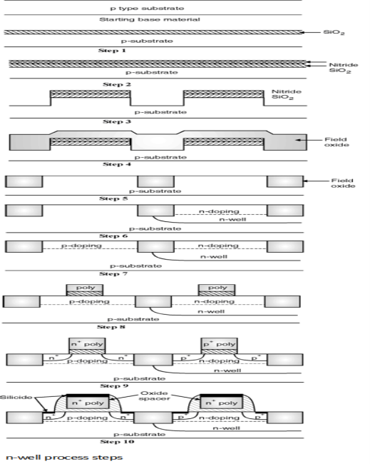
Figure 2. N well process
Q5) Explain the P well process?
A5) The fabrication steps of p well process are same as that of an n-well process except that instead of n-well a p-well is implanted . The process steps involved in p-well process are shown in Figure below. The process starts with the n type substrate.
Step 1 : A thin layer of SiO2 is deposited which will serve as the pad oxide.
Step 2 : A thicker sacrificial silicon nitride layer is deposited by chemical vapour deposition (CVD).
Step 3 : A plasma etching process is used to create trenches used for insulating the devices.
Step 4 : The trenches are filled with SiO2 which is called as the field oxide.
Step 5 : To provide flat surface chemical mechanical planerization is performed and also sacrificial nitride and pad oxide is removed.
Step 6 : The p-well mask is used to expose only the p-well areas, after this implant and annealing sequence is applied to adjust the well doping. This is followed by a second implant step to adjust the threshold voltage of the NMOS transistor.
Step 7 : Implant step is performed to adjust the threshold voltage of PMOS transistor.
Step 8 : A thin layer of gate oxide and polysilicon is chemically deposited and patterned with the help of polysilicon mask.
Step 9 : Ion implantation to dope the source and drain regions of the PMOS (p+) and NMOS (n+) transistors, this will also form n + polysilicon gate and p+ polysilicon gate for NMOS and PMOS transistors respectively. Hence this process is called as self aligned process.
Step 10 : Then the oxide and nitride spacers are formed by chemical vapour deposition.
Step 11 : In this step contact or via holes are etched, metal is deposited and patterned. After the deposition of last metal layer final passivation or overglass is deposited for protection.
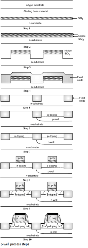
Figure 3. P well process steps
Q6) Explain the difference between the two?
A6) An important difference between p-well and n-well CMOS technologies is the doping levels of the substrate and well. Typical doping levels for the substrate material are approximately 2 x 10¹⁴ to 1015 cm-3. Since the wells are realized by means of diffusion, they are doped at a higher level than the substrate itself. Typical doping levels of the wells are about 1016 cm-3. As a result, the bulk doping level of an NMOS in a p-well CMOS technology is much higher than in an n-well CMOS technology. Typically this ratio is a factor of 10 to 50. These two values of bulk doping levels will give different values of transistor parameters.
Q7) Explain the twin tub process?
A7) In Dual-well process both p-well and n-well for NMOS and PMOS transistors respectively are formed on the same substrate. The starting material for this process is p+ substrate with epitaxially grown p-layer which is also called as epilayer.
The process starts with a p-substrate surfaced with a lightly doped p-epitaxial layer.
Step 1 : A thin layer of SiO2 is deposited which will serve as the pad oxide.
Step 2 : A thicker sacrificial silicon nitride layer is deposited by chemical vapour deposition.
Step 3 : A plasma etching process is used to create trenches used for insulating the devices.
Step 4 : The trenches are filled with SiO2 which is called as the field oxide.
Step 5 : To provide flat surface chemical mechanical planarization is performed and also sacrificial nitride and pad oxide is removed.
Step 6 : The p-well mask is used to expose only the p-well areas, after this implant and annealing sequence is applied to adjust the well doping. This is followed by second implant step to adjust the threshold NMOS transistor.
Step 7 : The n-well mask is used to expose only the n-well areas, after this implant and annealing sequence is applied to adjust the well doping. This is followed by a second implant step to adjust the threshold voltage of PMOS transistor.
Step 8 : A thin layer of gate oxide and polysilicon is chemically deposited and patterned with the help of polysilicon mask.
Step 9 : Ion implantation to dope the source and drain regions of the PMOS (p +) and NMOS (n+) transistors is used this will also form n+ polysilicon gate and p+ polysilicon gate for NMOS and PMOS transistors respectively.
Step 10 : Then the oxide or nitride spacers are formed by chemical vapour deposition (CVD).
Step 11 : In this step contact or holes are etched, metal is deposited and patterned. After the deposition of last metal layer final passivation or overglass is deposited for protection.
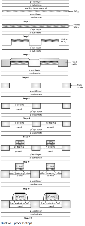
Figure 4. Twin tub process
Q8) Explain the layout of CMOS Inverter?
A8)
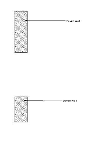
Figure 4. Device well
2. Draw a rectangle on the screen of the N-Well as shown below.
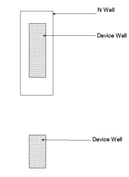
Figure 5. Nwell
3. Surround the N-WEll with the P-Guard.
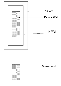
Figure 6. P Guard
4. Place the polysilicon gates.
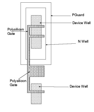
Figure 7. Polysilicon gate
5. Place the Ndope and Pdope masks, overlapping each other.
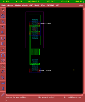
Figure 8.Masks
6. Add Metal1, Contacts, and Split Contacts.
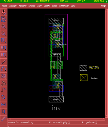
Figure 9. Metal contacts
7. Connect Input pin to the polysilicon gate.
8. Connect the Output pin to the metal 1 wire connecting the drains of the two transistors.
9. Connect the Metal 1 to Metal 2 using a "Via". Metal 2 is used for I/O connection purposes only.
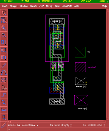
Figure 10. Complete circuit
Q9) Explain CMOS layout and design rules?
A9) The layout design rules provide a set of guidelines for constructing the various masks needed in the fabrication of integrated circuits. Design rules consist of the minimum width and minimum spacing requirements between objects on the different layers.
The most important parameter used in design rules is the minimum line width. This parameter indicates the mask dimensions of the semiconductor material layers. Layout design rules are used to translate a circuit concept into an actual geometry in silicon.
The design rules is the media between circuit engineer and the IC fabrication engineer. The circuit designers requires smaller designs with high performance and high circuit density whereas the IC fabrication engineer requires high yield process.
Minimum line width (MLW) is the minimum MASK dimension that can be safely transferred to the semiconductor material. For the minimum dimension design rules differ from company to company and from process to process.
To address this issue scalable design rule approach is used. In this approach rules are defined as a function of single parameter called ''. For an IC process '' is set to a value and the design dimensions are converted in the form of numbers. Typically a minimum line width of a process is set to 2 e.g. for a 0.25 m process technology '' equals 0.125 m.
Layered Representation of Layout :
The layer representation of layout converts the masks used in CMOS into a simple layout levels that are easier to visualise by the designers.
The CMOS design layouts are based on following components :
(1) Substrates or Wells : These wells are p type for NMOS devices and n type for PMOS devices.
(2) Diffusion regions : At these regions the transistors are formed and also called as active layer. These are defined by n+ for NMOS and p+ for PMOS transistors.
(3) Polysilicon layers : These are used to form the gate electrodes of the transistors.
(4) Metal interconnects layers : These are used to form the power supply and ground rails as well as input and output rails.
(5) Contact and Via layers : These are used to form the inter layer connections.
Q10) Explain silicon on insulator technology?
A10) Scaling of Bulk CMOS technology leads to issues such as sub-threshold leakage Power Parasitic device capacitances affecting the performance SOI technology and used in other devices like IGFETs
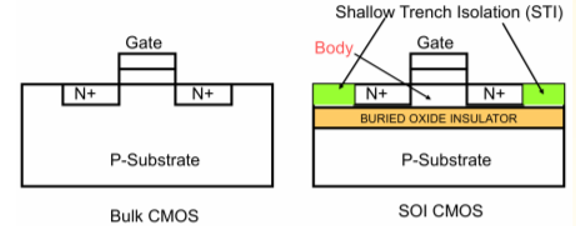
Figure 11. SOI CMOS
Unlike thin-film transistor, the top silicon layer of an SOI (silicon-on-insulator) wafer is high-quality single-crystalline material that is suitable for high-performance and high-density integrated. Many forms of SOI structures have been demonstrated with different insulator materials and holding substrates.
These include silicon-on-oxide, silicon-on-sapphire (SOS), silicon-on-zirconia (SOZ), and silicon on-nothing(air gap).
In SOS and SOZ technologies, a single-crystalline silicon film is epitaxially grown on a crystalline insulating substrate. In these cases, the insulators are the substrates themselves, Al2O3, in SOS and ZrO2, in SOZ.
Figure (a) shows a schematic diagram of an n-channel MOSFET made on an SOI substrate, with its typical I-Vcharacteristics shown in Fig. (b).
The kinks associated with floating body without a substrate tie are noticeable.
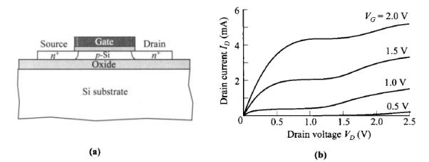
Figure 12. SOI substrate and V-I characteristics