Unit 5
Circuit Design using CPLD and FPGA
Q1) Explain CPLD and FPGA?
A1) A CPLD contains a bunch of PLD blocks whose inputs and outputs are connected by global interconnection matrix. So, a CPLD has two levels of programmability: each PLD block can be programmed, and then the interconnections between the PLDs can be programmed.
An FPGA takes a different idea. It has a clump of simple, configurable logic blocks arranged in an array with interspersed switches that can rearrange the interconnections between the logic blocks. Each logic block is individually programmed to perform a logic function such as AND, OR, XOR, etc. and then the switches are programmed to connect the blocks so that the complete logic functions are implemented.
Q2) Explain the architecture of CPLD?
A2) CPLD — Complex PLD that consists of an arrangement of multiple SPLD-like blocks on a single chip.
A CPLD comprises multiple circuit blocks on a single chip, with internal wiring re sources to connect the circuit blocks. Each circuit block is like a PLA or a PAL; An example of a CPLD is shown in Figure
It includes four PAL-like blocks that are connected to a set of interconnection wires. Each PAL-like block is also connected to a subcircuit labelled block, which is attached to several of the chip's input and output pins.
Figure shows an example of the wiring structure and the connections to a PAL-like block in a CPLD. The PAL-like block includes 3 macrocells each consisting of a four-input OR gate the real CPLDs usually provide between 5 and 20 inputs to each OR gate. The OR-gate output is connected to another type of logic. It is called an Exclusive-OR (XOR) gate. The behaviour of an XOR gate is the same as for an OR gate except that if both inputs are 1, the XOR gate produces a 0.
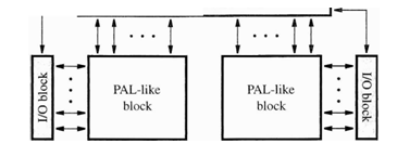
Figure. CPLD
Q3) Explain the architecture of FPGA?
A3) FPGA — a Field-Programmable Gate Array is an FPD featuring a general structure that allows extremely high logic capacity whereas CPLDs feature logic resources with a wide number of inputs (AND planes), FPGAs offer more narrow logic resources. FPGAs also offer a higher ratio of flip-flops to logic resources than CPLDs.
FPGAs comprise an array of uncommitted circuit elements, called logic blocks, and interconnect resources, but FPGA configuration is performed through programming by the end user. An illustration of a typical FPGA architecture appears in Figure. As the only type of FPD that supports extremely high logic capacity, FPGAs have been responsible for a major shift in the way digital circuits are designed.
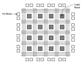
Figure. FPGA
Q4) Explain function block architecture?
A4) The CLBs consist of three essential elements: LUTs, multiplexer, Flipflop. The LUT is the primary element that can implement the logical function, and a multiplexer is used to select the data output between combinational and sequential logic. Flip Flops is being used for sequential logic implementation, as shown in Figure .
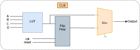
Figure : Configurable Logic Block Architecture
Q5) Explain interconnect?
A5)
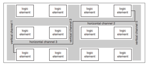
Figure. Interconnect
An FPGA designer must rely on pre-designed wiring, unlike a custom VLSI designer who can design wires as needed to make connections. logic element IOB interconnect logic element logic element IOB IOB logic element IOB interconnect logic element logic element IOB logic element IOB interconnect logic element logic element IOB interconnect Figure 3-1 Generic structure of an FPGA fabric. FPGA Architectures 107 The interconnection system of an FPGA is one of its most complex aspects because wiring is a global property of a logic design
Q6) Explain input output block?
A6)
Q7) Explain FPGA fabric?
A7) In general, FPGAs require three major types of elements: • combinational logic; • interconnect; • I/O pins
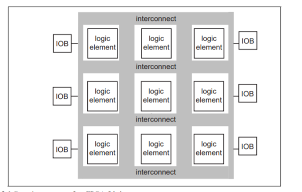
Figure.General strucrture of FPGA fabric
Figure shows the basic structure of an FPGA that incorporates these three elements. The combinational logic is divided into relatively small units which may be known as logic elements (LEs) or combinational logic blocks (CLBs). The LE or CLB can usually form the function of several typical logic gates but it is still small compared to the typical combinational logic block found in a large design. The interconnections are made between the logic elements using programmable interconnect. The interconnect may be logically organized into channels or other units. FPGAs typically offer several types of interconnect depending on the distance between the combinational logic blocks that are to be connected; clock signals are also provided with their own interconnection networks. The I/O pins may be referred to as I/O blocks (IOBs). They are generally programmable to be inputs or outputs and often provide other features such as low-power or high-speed connections.
Q8) Explain the architecture of Xilinx 9500 series ?
A8)
- High-performance
- Endurance of 10,000 program/erase cycles
- Program/erase over full commercial voltage and temperature range
- Enhanced pin-locking architecture
- Flexible 36V18 Function Block
- Slew rate control on individual outputs - User programmable ground pin capability
- Extended pattern security features for design protection
- High-drive 24 mA outputs
- 3.3V or 5V I/O capability
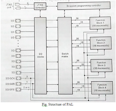
Figure. Xilinx 9500 series
Q9) Explain MAX 7000 series?
A9) The MAX 7000 architecture includes, 1) Logic array blocks 2) Macrocells, 3) Expander product terms, 4) Programmable interconnect array and 5) Input/Output control blocks. The MAX 7000 architecture is based on high performance logic array blocks consist of 16-macrocell arrays. Logic array blocks are linked together with the programmable interconnect array.
The MAX 7000 macrocell configured for sequential and combinational logic operation. In MAX 7000 macrocell the combinational logic is implemented in the logic array and provides five product terms per macrocell. Here, logic is routed between logic array blocks to programmable interconnect array.
Signals required by each logic array block are routed from the programmable interconnect array into the logic array block. EEPROM cell controls one input to a 2-input AND gate, and selects a programmable interconnect array signal to drive into the logic array block. The I/O control block for the MAX 7000 family leads to I/O pin configuration for input, output, or bidirectional operation. The I/O pins has tri-state buffer to control global output signals. The I/O control block of devices has two global output enable signals.
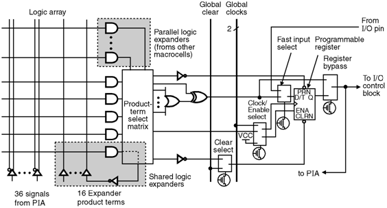 Figure. Altera-FLASH-logic-CPLDs
Q10) Explain Spartan 4000 architecture?
A10)
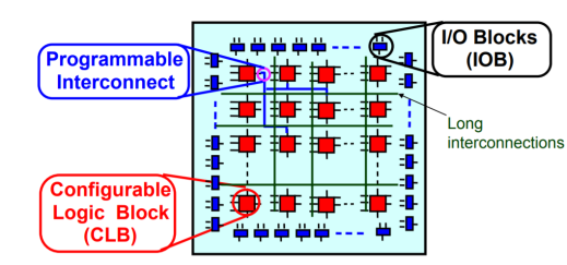
Figure. Xilinx Spartan 4000 archirtecture
Features:
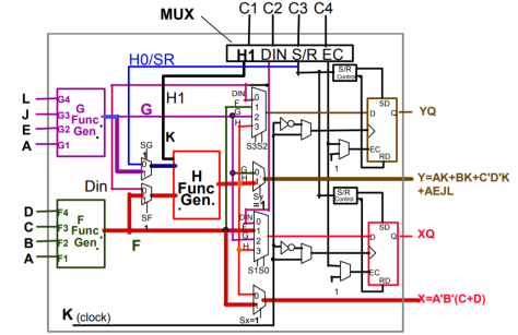
2 Four-input function generators (Look Up Tables) 1 Three-input function 2 Registers: - Pos. or Neg. edgetrig. Synchronous and asynchr. Set/Reset Possible functions: - any fct of 5 var. - two fcts of 4 var. + one fct of 3 var. - some fct of 9 var.
Implement the following functions on a single CLB of the XC4000 FPGA: X = A’B’ (C + D) Y = AK + BK + C’D’K + AEJL
