Unit 6
Design for Testability
Q1) What is fault model?
A1) A fault model is an engineering model that could go wrong in the construction or operation of a piece of equipment.
From the model, the designer or user can then predict the consequences of this particular fault.
Fault models can be used in almost all branches of engineering.
Basic fault models in digital circuits include:
- The stuck-at fault model.
In this, a signal, or gate output, is stuck at a 0 or 1 value, independent of the inputs to the circuit.
Here, two signals are connected together when they should not be. Depending on the logic circuitry employed, this may result in a wired-OR or wired-AND logic function. Since there are O(n2) potential bridging faults, they are normally restricted to signals that are physically adjacent in the design.
This model describes faults for CMOS logic gates. At transistor level, a transistor maybe stuck-short or stuck-open. In stuck-short, a transistor behaves as it is always conducts (or stuck-on), and stuck-open is when a transistor never conducts current (or stuck-off). Stuck-short will produce a short between VDD and VSS.
Here a wire is assumed broken, and one or more inputs are disconnected from the output that should drive them. As with bridging faults, the resulting behavior depends on the circuit implementation.
- The transition delay fault (or transition fault) model, where the signal eventually assumes the correct value, but more slowly (or rarely, more quickly) than normal.
Small-delay-defect mode
Q2) Explain the need for testability?
A2)
Q3) Explain path sensitizing?
A3)
The basic principle of the path sensitization method is to choose some path from the origin of the fault to the circuit output. A path is sensitized if the inputs to the gates along the path are assigned values such that the effect of the fault can be propagated to the output.
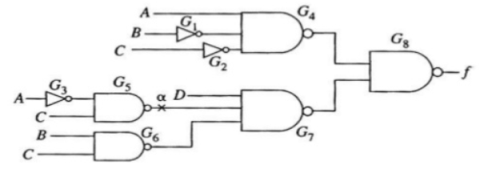
Figure. Path Sensitizing
From the above fig. Assume that the line α is s-a-1.
Hence to test for α, both G3 = C = 1. Also D = G6 =1 so that G7 =1 if the fault is absent. To propagate the fault from G7 to output f via G8 requires G4 = 1.
This is because if G4 = 0 then output f will be forced to be 1.
The process of propagating the effect of the fault from its original location to the circuit output is known as forward trace.
Similar is the process of backward trace.
Q4) Explain random tests?
Random pattern testing has been a common practice in industry for a long time. It was recognized quite early in the development of test generation strategies that there is a lot to be gained if a short random test precedes the long and laborious deterministic test.
A random test is defined as a random selection of input vectors. The input vectors may or may not be equally likely. A random test is said to be uniform if all input vectors are equally probable, and said to be biased otherwise. It is important to note that no test is truly random. The reason is that no ideal random number generator exists.
Q5) Explain BIST?
A5) As the complexity of VLSI circuits increases, test generation and application becomes an expensive and not always very effective means of testing. Built-in Self Test (BIST) is another solution.
It is a mechanism that permits a machine to test itself. Engineers design BISTs to meet requirements such as:
or constraints such as:
The main purposeof BIST is to reduce the complexity, and thereby decrease the cost and reduce reliance upon external (pattern-programmed) test equipment.
It reduces cost in two ways:
Figure below shows the Built-in Self Test system.
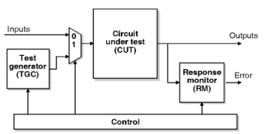
Figure. BIST
Q6) What is boundary scan test?
A6) In boundary scan test we design the chip to increase observability and controllability
If each register could be observed and controlled, test problem reduces to testing combinational logic between registers.
The logic blocks enter the test mode where they generate test patterns and report the results automatically.
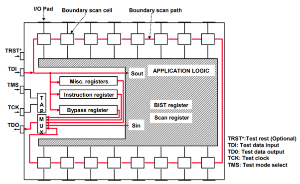
Figure. Boundary scan
Q7) What is fault coverage?
A7) Fault Coverage contains the percentage of faults detected from all the faults of the test patterns generated by the tool
FC = DT + (PD * posdet_credit) / Total faults x 100
where DT is the detected faults class which includes all the faults that the ATPG identifies as detected and this are classified into two groups
PD – posdet or possible detected fault class includes all the faults that fault simulation identifies as possible detected but not hard to detect
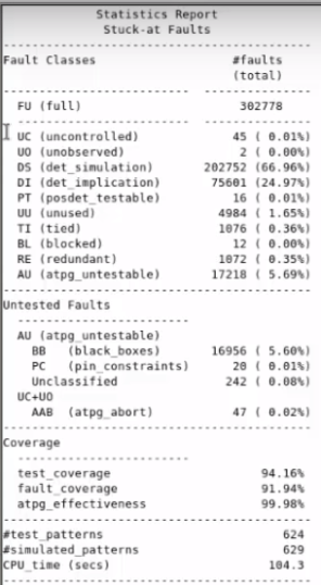
Figure. Report_statistics of faults
From the report Total no of faults are given as 302778
Faults due to unused pins (UU), Tied pins (TI), Blocked Pins (BL), and redundant logic (RE) are untestable by tool and this faults must be excluded from the total number of faults while calculating the Test Coverage and considered while calculating the Fault Coverage.
UU+TI+BL+RE => 4984+1076+12+1072 = 7144
Thus Testable faults are given asTotal Faults – (UU+TI+BL+RE)
Total faults detected during simulation (DS) and implication (DI) are
DS +DI => 202752+75601+16 = 278369
In generalposdet_credit will be set to zero and with this above faults numbers we can have Test Coverage and Fault Coverage
TC = DT +0 / Testable faults x 100
TC = 278369/ 302778-7144 x 100
TC = 94.16 %
FC = DT +0/ Total faults x 100
FC = 278369/302778 x 100
FC = 91.94%
In this process TC and FC are calculated and we need to achieve 99 % Test Coverage for Stuck At fault model and 95% Test Coverage for At Speed fault model.
Q8) What is stuck at fault model?
A8) With a stuck at fault model we apply a structural test approach. Instead of testing all combination of 1’s and 0’s to a VLSI device, we test with a reduced set of test vectors.
Stuck at Fault Models operate at the logic model of digital circuits. An input or an output can be Stuck at Zero (S@0) or Stuck at One (S@1).
Its use three digital circuits to illustrate: Inverter, NAND, NOR. In CMOS technology, these logic gates can be found in most logic functions.
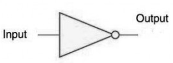
Logic table
A | D |
0 | 1 |
1 | 0 |
Inverter Stuck faults list: A S@0,A S@1, D S@0, D S@1
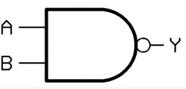
A | B | Y |
1 | 0 | 1 |
1 | 1 | 0 |
0 | 0 | 1 |
0 | 1 | 1 |
NAND Stuck faults list: A S@0,A S@1, BS@0, B S@1, CS@0, C S @1
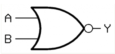
NOR Logic Table
A | B | Y |
1 | 0 | 1 |
1 | 1 | 0 |
0 | 0 | 1 |
0 | 1 | 1 |
NOR Stuck faults list: A S@0, A S@1, B S@0, B S@1, C S@0, C S@1
Q9) Explain stuck open and stuck short faults?
A9) Consider a 2-input NOR gate:
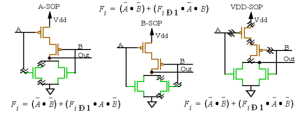
Figure. SOP model
First pattern initializes the output node, second pattern checks for the presence of the fault.

Figure . Stuck open model
In fault free circuit, this must be true rsince complementary logic functions drive BUS.
Stuck-short (Stuck-on) Faults
A transistor that is permanently stuck-on will, for some input combination(s), compete with its complementary transistors for control of the output.
Sometimes this competition does not result in a catastrophic failure.
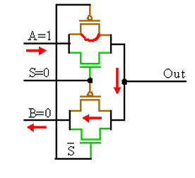
Figure. Stuck ON
The output value depends on driving transistor resistances. Strength of upstream drivers. Delay fault is likely if functional behaviour is preserved. IDDQ test guarantees detection.
Stuck-short faults modeled as SA0 on pMOS in gate-level equivalent model.
Q10) Explain boundary scan test?
A10) Boundary-scan cells in a device can capture data from integrated circuit line, or force data onto them. In this way a test system that can input a data stream to the shift register chain can set up states on the board, and also monitor data. By setting up one serial data stream, latching this into place, and then monitor the returning data stream, it is possible to gain access to the circuits on the board and check that a returning data stream is what is expected. If it is, then the test can pass, but if not the boundary scan system has detected and problem that can be further investigated.
Q11) Explain JTAG technology?
A11) The JTAG, boundary scan test technique uses a shift register latch cell built into each external connection of every boundary scan compatible device. One boundary scan cell is included in the integrated circuit line adjacent to each I/O pin, and when used in the shift register mode it can transfer data along to the next cell in the device. There are defined entry and exit points for the data to enter and exit the device, and it is therefore possible to chain several devices together.
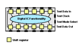
Figure. JTAG technology
Under normal operating conditions the cell is set so that it has no effect and it becomes invisible. However when the device is set to test mode, it permits a serial data stream (test vector) to be passed from one shift register latch cell to the next.
JTAG Interface
There are a number of JTAG control and data lines that form the test access port, TAP. These lines known as TCK, TMS and the optional TRST line are connected in parallel to the chips in the boundary scan chain. Connections designated TDI (input) and TDO (output) are daisy chained together to provide a path around the boundary scan chips for the data. Data is sent into the TDI of the first chip, and then TDO from the first chip is connected to TDI of the next and so forth. Finally the data is taken from the TDO of the last IC in the daisy chain.
Application:
It is used in a variety of other test scenarios, including product development and debugging as well as field service
Q12) Explain TAP controller?
A12) The TAP controller is a finite state machine that responds to changes at the TMS and TCK signals of the TAP and controls the sequence of operations of the circuitry defined by standard. It also controls the scanning of data into the various registers of the JTAG architecture. Two state transition paths for scanning the signal at TDI, one for shifting to the instruction register and one for shifting data into the active data register. The state diagram is shown in figure below. All state transitions of the TAP controller shall occur based on the value of TMS at the time of a rising edge of TCK. Actions of the test logic shall occur on either the rising or the falling edge of TCK in each controller state. The behavior of the TAP controller and other test logic in each of the controller states is briefly described as follows.
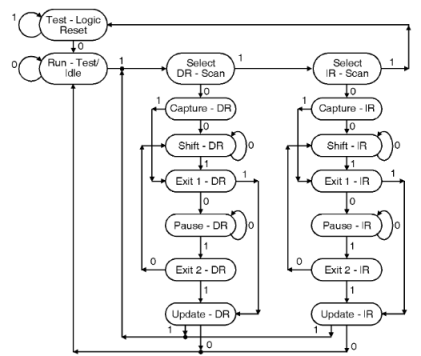
Figure . TAP controller