UNIT 3
Q.1.What do you understand by a semi-conductor? Discuss some important properties of semiconductor
Answer:
A semiconductor is a substance which has resistivity (10−4 to 0.5 Ωm) in-between conductors and insulators e.g. Germanium, silicon, selenium, carbon etc.
Nichrome, which is one of the highest resistance materials, has resistivity much lower than germanium. This shows that electrically germanium cannot be regarded as a conductor or insulator or a resistance material. This gave such substances like germanium the name of semiconductors. It is interesting to note that it is not the resistivity alone that decides whether a substance is semiconductor or not. For example, it is just possible to prepare an alloy whose resistivity falls within the range of semiconductors but the alloy cannot be regarded as a semiconductor. In fact, semiconductors have a number of peculiar properties which distinguish them from conductors, insulators and resistance materials.
Properties of Semiconductors
(i) The resistivity of a semiconductor is less than an insulator but more than a conductor.
(ii) (ii) Semiconductors have negative temperature co-efficient of resistance i.e. the resistance of a semiconductor decreases with the increase in temperature and vice-versa. For example, germanium is actually an insulator at low temperatures but it becomes a good conductor at high temperatures.
(iii) (iii) When a suitable metallic impurity (e.g. Arsenic, gallium etc.) is added to a semiconductor, its current conducting properties change appreciably.
Q.2.Which are the most commonly used semiconductors and why?
Answer:
The two most frequently used materials are germanium (Ge) and silicon (Si). It is because the energy required to break their co-valent bonds (i.e. energy required to release an electron from their valence bands) is very small; being about 0.7 eV for germanium and about 1.1 eV for silicon
Germanium. Germanium has become the model substance among the semiconductors; the main reason being that it can be purified relatively well and crystallised easily. Germanium is an earth element and was discovered in 1886. It is recovered from the ash of certain coals or from the flue dust of zinc smelters. Generally, recovered germanium is in the form of germanium dioxide powder which is then reduced to pure germanium.
The atomic number of germaniums is 32. Therefore, it has 32 protons and 32 electrons. Two electrons are in the first orbit, eight electrons in the second, eighteen electrons in the third and four electrons in the outer or valence orbit [See Fig. 5.2 (i)]. It is clear that germanium atom has four valence electrons i.e., it is a tetravalent element. Fig. 5.2 (ii) shows how the various germanium atoms are held through co-valent bonds. As the atoms are arranged in an orderly pattern, therefore, germanium has crystalline structure.
Silicon. Silicon is an element in most of the common rocks. Actually, sand is silicon dioxide. The silicon compounds are chemically reduced to silicon which is 100% pure for use as a semiconductor.
The atomic number of silicon is 14. Therefore, it has 14 protons and 14 electrons. Two electrons are in the first orbit, eight electrons in the second orbit and four electrons in the third orbit [See Fig. 5.3 (i)]. It is clear that silicon atom has four valence electrons i.e. it is a tetravalent element. Fig. 5.3 (ii) shows how various silicon atoms are held through co-valent bonds. Like germanium, silicon atoms are also arranged in an orderly manner. Therefore, silicon has crystalline structure
Q.3.Give the energy band description of semiconductors.
Answer:
In a semiconductor is a substance whose resistivity lies between conductors and insulators. The resistivity is of the order of 10−4 to 0.5-ohm meter. However, a semiconductor can be defined much more comprehensively on the basis of energy bands
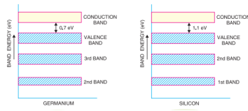
It may be seen that forbidden energy gap is very small; being 1.1 eV for silicon and 0.7 eV for germanium. Therefore, relatively small energy is needed by their valence electrons to cross over to the conduction band. Even at room temperature, some of the valence electrons may acquire sufficient energy to enter into the conduction band and thus become free electrons. However, at this temperature, the number of free electrons available is very small. Therefore, at room temperature, a piece of germanium or silicon is neither a good conductor nor an insulator. For this reason, such substances are called semiconductors. The energy band description is extremely helpful in understanding the current flow through a semiconductor.
Q.4. Discuss the effect of temperature on semiconductors?
Answer:
The electrical conductivity of a semiconductor changes appreciably with temperature variations. This is a very important point to keep in mind.
(i) At absolute zero.
At absolute zero temperature, all the electrons are tightly held by the semiconductor atoms. The inner orbit electrons are bound whereas the valence electrons are engaged in co-valent bonding. At this temperature, the co-valent bonds are very strong and there are no free electrons. Therefore, the semiconductor crystal behaves as a perfect insulator .In terms of energy band description, the valence band is filled and there is a large energy gap between valence band and conduction band. Therefore, no valence electron can reach the conduction band to become free electron. It is due to the non-availability of free electrons that a semiconductor behaves as an insulator.
(ii) Above absolute zero.
When the temperature is raised, some of the covalent bonds in the semiconductor break due to the thermal energy supplied. The breaking of bonds sets those electrons free which are engaged in the formation of these bonds. The result is that a few free electrons exist in the semiconductor. These free electrons can constitute a tiny electric current if potential difference is
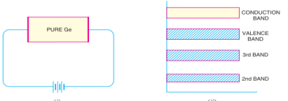
Applied across the semiconductor crystal. This shows that the resistance of a semiconductor decreases with the rise in temperature i.e. it has negative temperature coefficient of resistance. It may be added that at room temperature, current through a semiconductor is too small to be of any practical value.
Q.5 Define Fermi energy level. Explain Fermi Dirac distribution function ?
Answer:
When the material is at a temperature higher than OK, it receives thermal energy from surroundings i.e. electrons are thermally excited. As a result, they move into the higher energy levels which are unoccupied at OK. The occupation obeys a statistical distribution called Fermi – Dirac distribution law.
According to this distribution law, the probability F(E) that a given energy state E is occupied at a temperature T is given by

Here F(E) is called Fermi – Dirac probability function. It indicates that the fraction of all energy state (E) occupied under thermal equilibrium ‘K’ is Boltzmann constant.
Fermi Dirac distribution function:
Mathematically the probability of finding an electron in the energy state E at the temperature T is expressed as
Where, is the Boltzmann constant
T is the absolute temperature
Ef is the Fermi level or the Fermi energy
Now, let us try to understand the meaning of Fermi level. In order to accomplish this, put
in equation (1). By doing so, we get,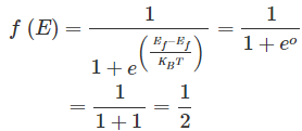
This means the Fermi level is the level at which one can expect the electron to be present exactly 50% of the time.
Q.6. What do you understand by intrinsic and extrinsic semiconductors?
Answer:
Intrinsic semiconductor
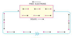
In an intrinsic semiconductor, even at room temperature, hole-electron pairs are created. When electric field is applied across an intrinsic semiconductor, the current conduction takes place by two processes, namely; by free electrons and holes. The free electrons are produced due to the breaking up of some covalent bonds by thermal energy. At the same time, holes are created in the covalent bonds. Under the influence of electric field, conduction through the semiconductor is by both free electrons and holes. Therefore, the total current inside the semiconductor is the sum of currents due to free electrons and holes.
Extrinsic semiconductor
The amount and type of such impurities have to be closely controlled during the preparation of extrinsic semiconductor.
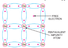
Generally, for 108 atoms of semiconductor, one impurity atom is added. The purpose of adding impurity is to increase either the number of free electrons or holes in the semiconductor crystal. As we shall see, if a pentavalent impurity (having 5 valence electrons) is added to the semiconductor, a large number of free electrons are produced in the semiconductor. On the other hand, addition of trivalent impurity (having 3 valence electrons) creates a large number of holes in the semiconductor crystal. Depending upon the type of impurity added,
Extrinsic semiconductors are classified into:
(i) n-type semiconductor
(ii) p-type semiconductor
Q .7. Explain Hall Effect in detail?
Answer:
When a material carrying current is subjected to a magnetic field in a direction perpendicular to direction of current, an electric field is developed across the material in a direction perpendicular to both the direction of magnetic field and current direction. This phenomenon is called “Hall-effect”.
Explanation:
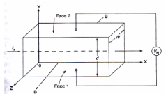
* Consider a semi-conductor, and current passes along the X-axis and a magnetic field Bz is applied along the Z-direction, a field Ey is called the Hall field which is developed in the Y-direction.
* In P- type semi-conductor, holes move with the velocity “V” in the “+”ve X-direction. As they move across the semiconductor the holes experience a transverse force ‘Bev’ due to the magnetic field.
* This force drives the holes down to the lower face. As a result, the lower face becomes +vely charged and –ve charge on the upper surface creating the hall field in the Y-direction. The Hall field exerts an upward force on holes equal to Ee.
* In the steady sate, two forces just balance and as a result, no further increase of + ve charge occurs on Face1.
* In N type semiconductor, the majority charge carriers are electrons experiences a force in the downward direction and lower face gets – vely charged. As a result, Hall field will be in the Y – direction.
Hall Coefficient:
Hall field𝐸𝐻, for a given material depends on the current density J and the applied magnetic field B.
i.e. 𝐸𝐻α JB
𝐸𝐻 = 𝑅𝐻 α JB
Since,
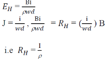
This is called hall coefficient.
Q.8 Explain zener diode?
Answer: A Zener diode is a silicon semiconductor device that permits current to flow in either a forward or reverse direction. The diode consists of a special, heavily doped p-n junction, designed to conduct in the reverse direction when a certain specified voltage is reached.
The Zener diode has a well-defined reverse-breakdown voltage, at which it starts conducting current, and continues operating continuously in the reverse-bias mode without getting damaged. Additionally, the voltage drop across the diode remains constant over a wide range of voltages, a feature that makes Zener diodes suitable for use in voltage regulation.
The Zener diode operates just like the normal diode when in the forward-bias mode, and has a turn-on voltage of between 0.3 and 0.7 V. However, when connected in the reverse mode, which is usual in most of its applications, a small leakage current may flow. As the reverse voltage increases to the predetermined breakdown voltage (Vz), a current starts flowing through the diode. The current increases to a maximum, which is determined by the series resistor, after which it stabilizes and remains constant over a wide range of applied voltage.
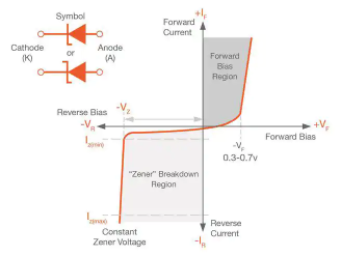
Zener breakdown
The breakdown is either due to the Zener breakdown effect that occurs below 5.5 V, or impact ionization that occurs above 5.5 V. Both mechanisms result in the same behavior and do not require different circuitry; however, each mechanism has a different temperature coefficient.
The Zener effect has a negative temperature coefficient while the impact effect experiences a positive coefficient. The two temperature effects are almost equal at 5.5 V and cancel out each other to make the Zener diodes rated at around 5.5 V the most stable over a wide range of temperature conditions
Q.9 Define mobility and current density?
Answer:
Mobility:
Dopants in an intrinsic semiconductor perform two major functions
1. They increase carrier concentration of a particular polarity (i.e. electrons or holes) so that the overall conductivity is higher. Usually this is orders of magnitude higher than the intrinsic semiconductor and is dominated by either electrons or holes i.e. the majority carriers.
2. Dopants also stabilize carrier concentration around room temperature. For Si, the saturation regime extends from roughly 60 K to 560 K.
Consider the general conductivity equation

For extrinsic semiconductors with either n or p much higher than the minority carrier concentration equation 1 can be written as

µe and µh are the drift mobilities of the carriers. They are given by

The drift mobilities are a function of temperature and in extrinsic semiconductors they depend on the dopant concentration.
Current density:
When an electric field E is applied across a semiconductor material, the charge
Carriers attain a drift velocity vd.
So, drift velocity
Vd=µE----------------(1)
The relation between current density J and drift velocity vd is
J=Nqvd
Where N is the carrier concentration
q is the charge of electron or hole
From equations (1) and (2), we get

_ is the mobility of charge carrier.
The above equation shows the general expression for drift current density.
Drift current density due to electrons is

Where is the electrons carrier concentration and
µe the mobility of electrons
Drift current density due to holes is

Total drift current density:

Q.10 what do you mean by direct and in direct band gap in semiconductor?
Answer:
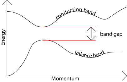
The band gap represents the minimum energy difference between the top of the valence band and the bottom of the conduction band; However, the top of the valence band and the bottom of the conduction band are not generally at the same value of the electron momentum. In a direct band gap semiconductor, the top of the valence band and the bottom of the conduction band occur at the same value of momentum.
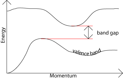
In an indirect band gap semiconductor, the maximum energy of the valence band occurs at a different value of momentum to the minimum in the conduction band energy:
