Unit - 3
Data Processing Circuits
Q1) What is Multiplexer?
A1)
A multiplexer is a combinational logic circuit that connects one or more input lines to a single output line.
The action of delivering one or more analogue or digital signals over a common transmission line at different times or speeds is referred to as multiplexing, and the equipment we use to do so is referred to as a multiplexer.
The multiplexer, abbreviated as "MUX" or "MPX," is a combinational logic circuit that uses a control signal to switch one of numerous input lines to a single common output line. Multiplexers work like highly rapid acting multiple position rotary switches, connecting or regulating several input lines, referred known as "channels," to the output one at a time.
Multiplexers, often known as MUXs, are digital circuits that employ high-speed logic gates to switch digital or binary data, or analogue circuits that employ transistors, MOSFETs, or relays to switch one of the voltage or current inputs to a single output.
A one-way rotary switch, as pictured, is the simplest basic sort of multiplexer device.
Q2) What is 4 Channel Multiplexer using Logic Gates?
A2)
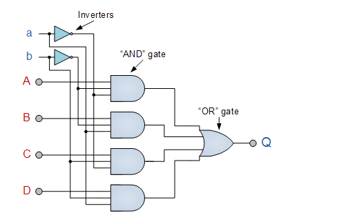
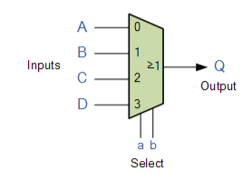
A multiplexer is represented by the following symbol in logic diagrams:
Symbol for a Multiplexer
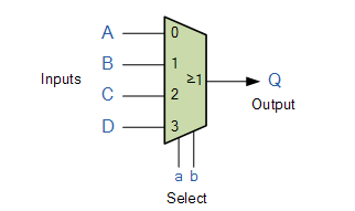
Multiplexers can do more than merely combine a number of various input lines or channels into a single output. There are also varieties that may switch their inputs to numerous outputs, such as 4-to-2, 8-to-3, or even 16-to-4, and an example of a simple Dual channel 4 input multiplexer (4-to-2) is shown below:
Q3) Explain Working Principle of 2 to 1 Multiplexer and Give its Truth Table.
A3)
When S=0, it is used as a direct input to the second AND gate, and when S=1, it is used as a second input to the first AND gate. We now know that if any one of the AND gate's inputs is zero, the output is also zero. As a result, the second AND gate's output is zero. The output of the first AND gate is identical to its first input, which is Y = D0, because the second input is 1.
When S=1, the exact opposite occurs. The second AND gate output is identical to the first AND gate input in this case, Y = D1, and the first AND gate output is 0.
We may select the proper input, D0 or D1, by supplying a logic ‘0' or ‘1' to the select input S, making the circuit operate as a single pole double throw (SPDT) switch.
2 to 1 Multiplexer Truth Table
The below table shows the truth table for the 2-to-1 multiplexer.
Select input S | Data Input  | Data Input  | Output Y |
0 | 0 | 0 | 0 |
0 | 0 | 1 | 0 |
0 | 1 | 0 | 1 |
0 | 1 | 1 | 1 |
1 | 0 | 0 | 0 |
1 | 0 | 1 | 1 |
1 | 1 | 0 | 0 |
1 | 1 | 1 | 1 |
Truth Table of 2-to-1 Multiplexer
The 2-input multiplexer creates a 2-to-1 multiplexer by connecting one of two 1-bit sources to a shared output.
Q4) Explain Working Principle of 8 to 1 Multiplexer and Give its Truth Table.
A4)
The topmost AND gate is enabled and all other AND gates are disabled if all three select inputs are S0 = 0, S1 = 0, S3 = 0. As a result, the data input D0 is chosen and sent as an output. As a result, we receive the result Y = D0.
The bottom-most AND gate is enabled and all other AND gates are disabled if all three select inputs are S0 = 1, S1 = 1, S3 = 1. As a result, the data input D7 is chosen and sent as an output. As a result, we have output Y = D7.
8 to 1 Multiplexer Truth Table
The below table shows the truth table for the 8-to-1 multiplexer.
S0 | S1 | S2 | Y |
0 | 0 | 0 | D0 |
0 | 0 | 1 | D1 |
0 | 1 | 0 | D2 |
0 | 1 | 1 | D3 |
1 | 0 | 0 | D4 |
1 | 0 | 1 | D5 |
1 | 1 | 0 | D6 |
1 | 1 | 1 | D7 |
Truth Table of 8-to-1 Multiplexer
Q5) What is a Multiplexer Tree or Chaining Multiplexers?
A5)
Multiplexers with a larger number of inputs can be generated by cascading two or more multiplexers with fewer inputs.
In other words, larger multiplexers can be made by chaining smaller multiplexers together. A multiplexer tree or a chaining multiplexer is what this is called.
Two 4-to-1 and one 2-to-1 multiplexers, for example, can be cascaded to create an 8-to-1 multiplexer. The output of the two 4-to-1 multiplexers is fed into the 2-to-1 multiplexer, and the select lines on the 4-to-1 multiplexers are connected in parallel, resulting in a total of three select inputs, comparable to an 8-to-1 multiplexer. Let's have a look at an example.
Example: Using two 4-to-1 multiplexers, create an 8-to-1 multiplexer.
Solution:
- The 8-to-1 multiplexer is created by cascading two 4-to-1 multiplexers, as shown in the diagram below.
- There are eight data inputs, numbered D0 through D7.
- Both 4-to-1 multiplexers' select inputs S0 and S1 are connected in parallel, while the third select input S2 is utilised to enable one multiplexer at a time.
- Choose your input. S2 is connected directly to MUX-1's Enable(E) terminal, while S2– is attached to MUX-2's enable terminal.
- To achieve the final output Y, the outputs of both multiplexers are connected to the OR gate.
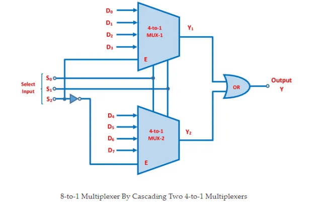
Fig. 8-to-1 Multiplexer By Cascading 4-to-1 Multiplexers
The truth table is shown in the below table. We get the output, and when MUX-1 is enabled and when MUX-2 enabled.
S0 | S1 | S2 | Y |
0 | 0 | 0 | D0 |
0 | 0 | 1 | D1 |
0 | 1 | 0 | D2 |
0 | 1 | 1 | D3 |
1 | 0 | 0 | D4 |
1 | 0 | 1 | D5 |
1 | 1 | 0 | D6 |
1 | 1 | 1 | D7 |
Q6) Explain Types of Binary Decoders.
A6)
In essence, a Decoder is a combinational logic circuit that translates coded input to coded outputs when both of these are distinct. The term "decoder" refers to a device that converts coded data from one format to another. As a result, the input code has less bits than the output code word.
A digital decoder is a device that translates a set of digital signals into decimal code. Prior to the advent of an encoder, a decoder was a regularly utilised circuit. After the information is encoded by encoders, it is decoded for user interface in most output devices such as monitors, calculator displays, printers, and so on. We'll look at numerous sorts of binary decoders in this article.
Binary Decoders
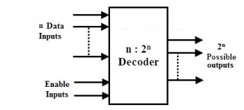
A binary decoder is a multi-input, multi-output combinational circuit that converts a binary code of n input lines into a one out of 2n output code. When an n-bit input value is needed to activate exactly one of 2n outputs, these are employed.
The diagram below depicts the overall structure of a binary decoder, which accepts encoded data on n input lines and produces output on 2n potential output lines.
Enable inputs are typically included with decoders to activate the decoded output based on data inputs. In BCD coding, for example, the four bit combinations 0000 through 1001 are sufficient to represent the decimal numbers 0 to 9.
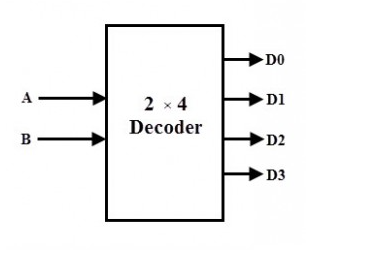
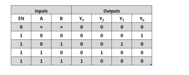
2-to-4 Binary Decoder
Two inputs are decoded into four outputs in a 2-to-4 binary decoder, which has two input lines and four output lines. At any one time, only one output is active, while the others are kept at logic 0, and the output that is kept active or high is controlled by the two binary inputs A and B.
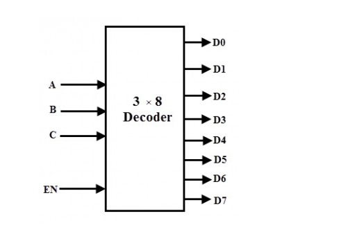
3-to-8 Decoder
Three inputs are processed into eight outputs in a 3-to-8 decoder. It has three inputs as A, B, and C and eight output from Y0 through Y7. Only one of the eight outputs is chosen based on the combinations of the three inputs.
4-to-16 Decoder
A 4-to-16 decoder has four inputs and sixteen outputs. Like all of the previous decoders, just one output will be low at any given moment, while all other outputs will be high (using maxterms).
This type of decoder's truth table is illustrated below. If the decoder's input is 1000, output Y8 will be low, while all other outputs will be high, as illustrated in the diagram. This will continue to be the case for all input combinations.
Q7) Write the Applications of Digital Encoder.
A7)
1. Keyboard Encoder
Priority encoders can be used in circuits or applications with many inputs to reduce the number of wires required. Assume that a microcomputer needs to read the 104 keys on a normal QWERTY keyboard, where only one key is touched at a time, either "HIGH" or "LOW."
One option is to link all 104 wires from the individual keys on the keyboard to the computer's input directly, although this is difficult for a tiny home PC. Another, better option is to use a priority encoder to connect the keyboard to the computer.
To represent each key or character on the keyboard, the 104 separate buttons or keys could be converted into a conventional ASCII code of only 7 bits (0 to 127 decimal) and then directly input to the computer as a considerably smaller 7-bit B.C.D code. To do so, keypad encoders like the 74C923 20-key encoder are available.
2. Positional Encoders
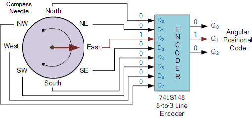
Magnetic positional control, such as that used on ships or for robotic arm positioning, is another more widespread application. A 74LS148 8-to-3 line priority encoder, for example, converts the angular or rotational position of a compass into a digital code that is then entered to the systems computer to provide navigational data, and an example of a simple 8 position to 3-bit output compass encoder is shown below. To show the needles' angular location, magnets and reed switches could be employed at each compass point.
3. Priority Encoder Navigation
Q8) Write Short note on Binary Subtract.
A8)
The Binary subtractor is a circuit that conducts the subtraction of two binary numbers. The binary subtractor can be implemented using one of the two approaches below.
2's complement approach with cascade full subtractors
By cascading ‘n' Full subtractors, we can create an n-bit binary subtractor in the first approach. So, similar to Half adder and Full adder, you may start by implementing Half subtractor and Full subtractor. Then, by cascading ‘n' Full subtractors, you can create an n-bit binary subtractor. So, for binary addition and subtraction of two binary numbers, we'll have two different circuits.
In the second way, we can subtract two binary values with the same binary adder by making a few changes to the second input. As a result, a binary addition operation is performed internally, but the output is resulting subtraction.
The subtraction of two binary values A and B can be expressed as, as we know.
A−B=A+(2′scomplimentofB)
⇒A−B=A+(1′scomplimentofB)
4-bit Binary Subtract
Two 4-bit values are subtracted using the 4-bit binary subtractor. Let A=A3A2A1A0A=A3A2A1A0 and B=B3B2B1B0B=B3B2B1B0 be the 4bit binary numbers. The functioning of the 4-bit Binary subtractor is similar to that of the 4-bit Binary adder on the inside. When the normal bits of binary number A, the complemented bits of binary number B, and the initial carry borrow, Cin are applied as one to a 4-bit Binary adder, the result is a 4-bit Binary subtractor. The following diagram depicts the block diagram of a 4-bit binary subtractor.
This 4-bit binary subtractor generates an output with a maximum of 5 bits. If Binary number A is bigger than Binary number B, the output's MSB is zero, and the remaining bits contain the A-B magnitude. The output's MSB is one if Binary number A is less than Binary number B. To find the magnitude of A-B, take the 2's complement of the output.
By cascading the requisite number of Full adders with the relevant modifications, we may create any higher order binary subtractor.
Q9) Explain 4-bit Binary Adder in Short.
A9)
The addition of two 4-bit values is performed using the 4-bit binary adder. Let A=A3A2A1A0A=A3A2A1A0 and B=B3B2B1B0B=B3B2B1B0 be the 4-bit binary numbers. The 4-bit binary adder can be implemented in one of two ways.
● For the addition of two least significant bits, use one Half adder, and three full adders for the addition of three higher significant bits.
● For consistency, use four full adders. Because the initial carry Cin is zero, the Half adder is utilised to add the least significant bits instead of the Full adder.
● We examined the second method for the time being. The following diagram depicts the block diagram of a 4-bit binary adder.
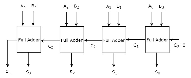
The four full adders are cascaded here. Each Full adder receives the bits from two parallel inputs A and B. The carry input of the next higher order Full adder will be the carry output of the previous Full adder. The output sum of this 4-bit binary adder has a maximum of 5 bits. As a result, the MSB will carry out the last step Full adder.
We can create any higher order binary adder by cascading the needed number of Full adders in this fashion. Because the carry propagates ripple from one stage to the next, this binary adder is also known as a ripple carry binary adder.
Q10) What is Binary Arithmetic Circuits?
A10)
The Half Adder
Combinal logic circuits perform binary arithmetic, the simplest of which is the half adder, as shown in Fig. In its most basic form, this circuit consists of two gates: an XOR gate and a logic 1 output whenever A is 1 and B is 0, or when B is 1 and A is 0. When both A and B are 1, the AND gate produces a logic 1 at the carry output. Table shows the half adder truth table, which describes the result of binary addition.
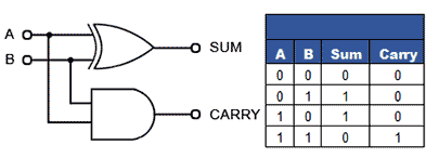
Fig: The Half Adder
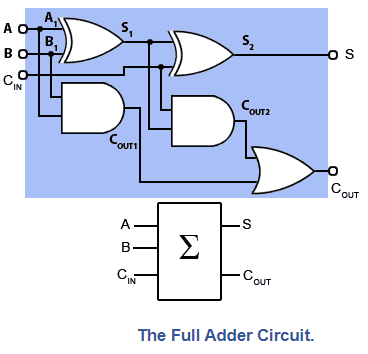
Fig: The Full Adder Circuit
1 plus 0 = 12 (110)
And
1 plus 1 = 102 (210)
The half adder is fine for adding two 1-bit numbers together, but for binary numbers containing several bits, a carry may be produced at some time (as a result of adding 1 and 1) that must be added to the next column. Because the half adder only has two inputs, it can't add in a carry bit from a previous column, hence it's only good for 1-bit adds.
The Full Adder
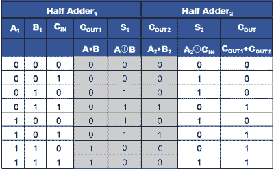
The Full Adder, illustrated in Fig. (blue backdrop) with its simplified block diagram symbol, is used when two or more bits need to be added. This circuit consists of two half adders, with the first half adder's total of A and B serving as input A to the second half adder, which creates a sum of the first half adder sum (S1) plus any "carry in" from the CIN terminal. The two half adders' carries are then 'ORed' together to form a single COUT. Output. Table shows the truth table for the circuit.
Parallel Adders
Even though a full adder only adds two single bit binary integers, it can be paired with other full adders to create parallel adders that add two multibit integers. To add multibit binary values, parallel adders can be created in a variety of ways, with each bit of the parallel adder employing a single full adder circuit. Because drawing parallel adder circuits with all of the individual gates would be extremely complicated, it is usual to replace the full adder schematic diagram with a simplified block diagram version.
Bit Parallel Adder
Because any carry appearing at the carry in input (CIN) or produced when adding any of the 4-bit inputs ‘ripples' throughout the adder stages until a final carry out emerges at the carry out output (COUT) of the final full adder for bit A3+B3, Fig is also known as a ‘Ripple Carry Adder.'
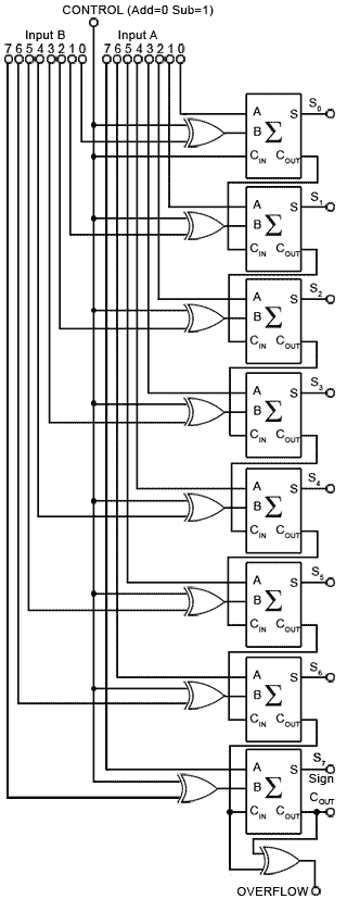
Fig. 8−Bit Twos Complement Adder/Subtractor.
Q11) Explain Addition Using 2s Complement.
A11)
Addition using 2's complement
When we add two binary numbers using 2's complement, there are three potential instances that can occur:
Case 1: Addition of the positive number with a negative number when the positive number has a greater magnitude.
Find the two's complement of the given negative number first. Add the specified positive number to the total. The number will be a positive number if we get the end-around carry 1, and the carry bit will be discarded, leaving the remaining bits as the final result.
Example: 1101 and -1001
1. To begin, determine the negative integer 1001's 2's complement. To find the 2's complement, turn all 0s to 1s and all 1s to 0s, or find the 1's complement of 1001. Add 1 to the LSB of the result 0110 to get the 1's complement of the number 1001. As a result, the 2's complement of 1001 is 0110+1=0. 112
2. Add the numerals 1101 and 0111 together; 1101+0111=1 0100
3. We get the end-around carry 1 by adding both values. The end-around carry is discarded. As a result, the sum of both numbers equals 0100.
Case 2: Adding of the positive value with a negative value when the negative number has a higher magnitude.
To begin, add a positive value to the negative number's 2's complement value. There is no end-around carry here. To get the final result, we take the 2's complement of the result.
1. Find the negative number 1110's 2's complement first. Add 1 to the LSB of the 1's complement value 0001 to discover 2's complement. 0001+1=0010
2. Add the numbers 1101 and 0010 together.
1101 plus 0010 equals 1111.
3. Find the 2's complement of the final result, which is 1110. As a result, the 2's complement of the result 1110 is 0001, and we can tell it's a negative integer by adding a minus sign before it.
Case 3: Addition of two negative numbers
In this example, we'll find the 2's complement of both negative values, then add the two complement numbers together. In this scenario, we'll always obtain the end-around carry, which will be added to the LSB, and we'll take the 2's complement of the result instead of the final result.
Example: -1101 and -1110 in five-bit register
1. First, determine the negative numbers 01101 and 01110's 2's complement. So, to determine 2's complement, we add 1 to the LSB of these integers' 1's complement. 01110 has a 2's complement of 10010, and 01101 has a 2's complement of 10011.
2. We multiply both complement numbers, 10001 and 10010, to get 1 00101; 10010+10011= 1 00101
3. We get the end-around carry 1 by adding both values. The carry is removed, and the final result is the 2.s complement of 00101. As a result, the 2's complement of 00101 is 11011, and we append a negative sign before the number to indicate that it is a negative number.
Addition with the 2's complement
To subtract two binary numbers using 2's complement, follow these steps.
o Find the 2's complement of the subtrahend in the first step.
o Take the complement number and multiply it by the minuend.
o If we receive the carry by adding both integers, we ignore it and the result is positive; otherwise, we take the result's 2's complement, which is negative.
Q12) What is Half Adder?
A12)
A and B are the two inputs of the half adder circuit, which add two input digits and output a carry and a sum. The full adder circuit contains three inputs: A, B, and C, which add three values and provide a carry and sum. This article provides thorough information in tabular form as well as circuit diagrams on what a half adder and full adder are used for. The primary and most important function of adders has previously been discussed. The half adder and full adder theories are explained below.

Fig: Basic half adder and full adder
Half Adder
So, in the case of a half adder, it adds two binary digits, where the input bits are referred to as augend and addend, and the result is two outputs, one of which is the sum and the other of which is the carry. XOR is used to both inputs to execute the sum operation, while AND gate is applied to both inputs to provide carry.
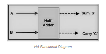
The full adder circuit, on the other hand, adds three one-bit values, with two of the three bits referred to as operands and the other as bit brought in. Output carry and sum are terms used to describe the 2-bit output that is produced.
With the help of logic gates and a half adder, you can design simple addition.
Let's look at an example of how to add two single bits.
The truth table for a 2-bit half adder is as follows:
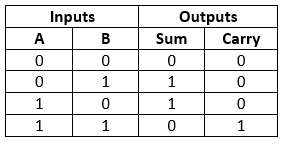
0+0 = 0
0+1 = 1
1+0 = 1
1+1 = 10
These are the least possible single-bit combinations. But the result for 1+1 is 10, the sum result must be re-written as a 2-bit output. Thus, the equations can be written as
0+0 = 00
0+1 = 01
1+0 = 01
1+1 = 10
The output ‘1’of ‘10’ is carry-out. ‘SUM’ is the normal output and ‘CARRY’ is the carry-out.
It has now been established that a 1-bit adder can be simply created using an XOR Gate for the ‘SUM' output and an AND Gate for the ‘Carry' output.
When we need to add two 8-bit bytes together, for example, we can use a full-adder logic circuit. When you need to add one binary digit quantities, the half-adder comes in handy.
Making a truth table and reducing it is one technique to construct two-binary digit adders. The half adder addition action is repeated twice to create a three binary digit adder. Similarly, if you want to construct a four-digit adder, you must repeat the process once more. With this hypothesis, it was evident that implementation would be straightforward, but development would take time.
The exclusive OR function is used in the simplest expression:
Sum= A XOR B
Carry = A AND B
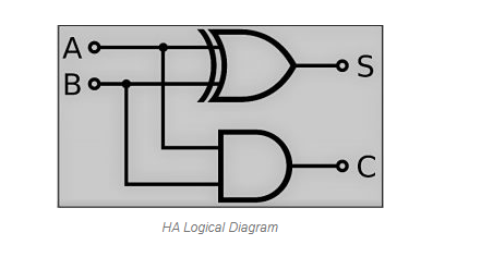
And an equivalent expression in terms of the basic AND, OR, and NOT is:
SUM=A.B+A.B’
VHDL Code For Half Adder
Entity ha is
Port (a: in STD_LOGIC;
b : in STD_LOGIC;
Sha : out STD_LOGIC;
Cha : out STD_LOGIC);
End ha;
Architecture Behavioral of the above circuit is
Begin
Sha <= a xor b;
Cha <= a and b;
End Behavioral
Q13) Write Difference between Half Adder and Full Adder.
A13)
The difference between the half adder and full adder table is shown below.
Half Adder | Full Adder |
The Half Adder (HA) is a combinational logic circuit that is used to add two one-bit numbers together. | The Full Adder (FA) is a combinational circuit that adds three one-bit digits together. |
In HA, once the carry from the previous addition is generated, it cannot be added to the following step. | Once the carry has been generated from the previous addition, it can be applied to the following step in FA. |
The half adder has two logic gates, the AND and EX-OR gates. | Two EX-OR gates, two OR gates, and two AND gates make up the whole adder. |
The half adder takes two input bits, A and B. | The complete adder has three input bits, A, B, and C-in. |
Half adder sum and carry equation is S = a⊕b ; C = a*b | Full adder logic expression is S = a ⊕ b⊕Cin; Cout = (a*b) + (Cin*(a⊕b)). |
HA is found in computers, calculators, and digital measurement instruments, among other things. | Digital processors, multiple bit addition, and other applications use FA. |
Q14) Explain Full Adder Implementation using Half Adders.
A14)
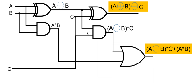
A FA can be implemented with two logically connected half adders. The connecting of an FA utilising two half adders is illustrated in the block diagram below.
The sum and carry equations from previous calculations are
S = A‘ B’ Cin + A’ BC’ in + ABCin
Cout = AB + ACin + BCin
The sum equation can be written as.
Cin (A’B ‘+ AB) + C ‘in (A‘B + A B’)
So, Sum = Cin EX-OR (A EX-OR B)
Cin (A EX-OR B) + C’in (A EX-OR B)
= Cin EX-OR (A EX-OR B)
Cout can be written like the following.
COUT = AB + ACin + BCin.
COUT = AB + ACin+ BCin (A + ̅A)
= ABCin + AB + ACin + A’ B Cin
= AB (1 + Cin) + ACin + A’ B Cin
= A B + ACin + A’ B Cin
= AB + ACin (B + B’ ) + A’ B Cin
= ABCin + AB + A’B Cin+ A’ B Cin
= AB (Cin + 1) + A B Cin + A’ B Cin
= AB + AB’ Cin + A’ B Cin
= AB + Cin ( AB’ + A’B )
Therefore, COUT = AB + Cin (A EX-OR B)
Depending on the above two sums & carry equations, the FA circuit can be implemented with the help of two HAs & an OR gate. A complete adder with two half adders is shown in the circuit diagram above.
Q15) Write Advantages of Full Adder.
A15)
The following are some of the benefits of using a half adder or a full adder.
1. A half adder's primary function is to add two single-bit values.
2. Full adders are capable of adding a carry bit, which is the result of the previous addition.
3. Critical circuits such as adder, multiplexer, and many more can be built with a full adder.
4. The entire adder circuits use very little power.
5. The advantages of a full adder over a half adder are that a full adder is used to overcome the disadvantages of a half adder, which is that the half adder is primarily used to add two 1-bit values. Because half adders don't add the carry bit, a full adder is used to compensate. Three bits can be added in a full adder, which yields two outputs.
6. Adders are straightforward to design and are a fundamental building block for understanding one-bit addition.
7. By adding an inverter, this adder can be transformed to a half subtractor.
8. High output can be produced by utilising a full adder.
9. Quickness
10. The ability to offer voltage scaling is really powerful.
Q16) What is Full Subtractor?
A16)
Only two numbers are subtracted with the Half Subtractor. A complete subtractor was created to solve this problem. To subtract three 1-bit values A, B, and C, which are minuend, subtrahend, and borrow, respectively, the full subtractor is employed. The full subtractor has three states of input and two states of output, diff and borrow.
Block diagram

Truth Table
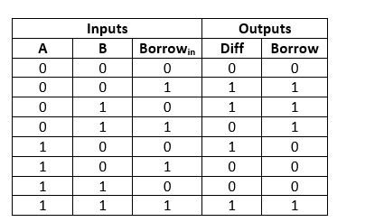
The input variables in the above table are o 'A' and 'B'. The two significant bits that will be removed are represented by these variables.
o The third input, 'Borrowin,' stands for borrow.
o The output variables 'Diff' and 'Borrow' provide the output values.
o The eight rows under the input variable represent all conceivable 0 and 1 combinations in these variables.
The Full subtractor circuit is built as shown in the block diagram above. The OR gate is used to join two half adder circuits in the circuit shown above. A and B are two single-bit binary inputs in the first half subtractor. The half subtractor, as we all know, has two outputs: 'Diff' and 'Borrow.' The first subtractor's 'Diff' output will be the second half subtractor's first input, and the first subtractor's 'Borrow' output will be the second half subtractor's second input. 'Diff' and 'Borrow' will be provided by the second half subtractor once more. The 'Diff' bit is the result of the Full subtractor circuit. We feed the 'Borrow' of the first and second subtractors through the OR gate to determine the final output of the 'Borrow'. The final carry 'Borrow' of the entire subtractor circuit will be the result of the OR gate.
The final 'Borrow' bit represents the MSB.
The whole subtractor logic circuit can be built using an OR gate and the AND, XOR, and NOT gates.
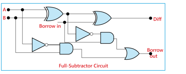
The whole subtractor's actual logic circuit is depicted in the diagram above. A Boolean expression can also be used to represent the complete subtractor circuit.
Diff: o Combine inputs A and B using the XOR method.
o Using 'Borrow,' perform an XOR operation on the result. As a result, the difference is (A XOR B) XOR 'Borrowin,' which can also be written as:
'Borrowin' (A) 'Borrowin' (B) 'Borrowin' (A) 'Borrowin'
Q17) Write the Advantages and Limitations of Half Subtractor.
A17)
The advantages of half subtractor are:
1. This circuit's implementation and construction are simple and straightforward.
2. In digital signal processing, this circuit uses very little power.
3. Computational functions can be carried out at a faster rate.
4. The following are the constraints of this combinational circuit:
5. Despite the fact that the half subtractor has numerous applications in a variety of operations and functionality, it does have a few restrictions, which are as follows:
6. The half subtractor circuits do not accept "borrow-in" from earlier outputs, which is the circuit's most significant flaw.
7. Because many real-time applications require the subtraction of a large number of bits, half subtractors devices are incapable of doing so.
Half Subtractor Applications
The following are some of the half subtractor's applications.
1. A half subtractor is a device that is used to lower the strength of audio or radio signals.
2. It can be used to minimise sound distortion in amplifiers.
3. In the processor's ALU, a half subtractor is used.
4. It also calculates addresses and can be used to increase and decrease operators.
5. The least significant column numbers are subtracted with a half subtractor. It can be used for multi-digit numeric subtraction with the LSB.
6. Finally, we may conclude from the previous half subtractor theory that by employing this circuit, we may subtract one binary bit from another to produce outputs such as Difference and Borrow. Similarly, both NAND and NOR gates can be used to create a half subtractor.
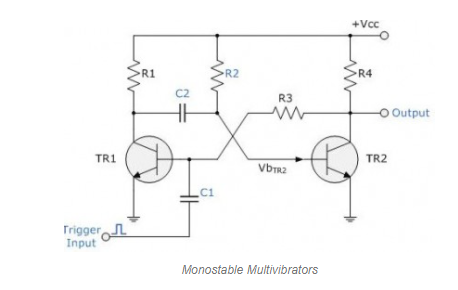
Q18) Explain Monostable Multivibrator.
A18)
When an external trigger pulse is delivered, monostable multivibrators have only one stable state, which is utilised to generate a single o/p pulse of a defined width, either high or low. This trigger pulse initiates a timing cycle, causing the o/p to change state at the start of the timing cycle and then continue in the second state determined by the capacitor C and resistor R time constants until it returns to its original state. It will stay in this mode until it receives another i/p signal. Monostable multivibrators can generate a rectangular waveform that is substantially longer. When a trigger pulse is applied externally, the waveform's leading edge rises in response to the external trigger. The RC time constant of the feedback components utilised determines the trailing edge. This RC time constant can be changed over time to generate a series of pulses with a fixed time delay compared to the initial triggering pulse.
Q19) Write the Working of Monostable Multivibrator with 555 Timer Circuit.
A19)
1. Until it receives a trigger, the output of the monostable multivibrator employing the 555 timer remains stable.
2. When both the transistor and the capacitor are shorted in a monostable 555 multivibrator, this is referred to be a stable state.
3. When the voltage on the 555 IC's second pin falls below a certain threshold, the o/p turns high. This high state is referred to as quasi-stable. When the circuit is turned on, it switches from a stable to a quasi-stable condition.
4. The discharge transistor is then turned off, and the capacitor begins to charge to VCC. The capacitor is charged through the resistor R1 with the time constant R1C1.
5. As a result, as the capacitor voltage rises and eventually exceeds 2/3 Vcc, the internal control flip flop changes, turning off the 555 timer IC.
6. As a result, the o/p returns to its stable condition after being in an unstable condition.
7. Finally, we can deduce that the o/p in the monostable multivibrator with 555 timer remains low until it receives a trigger i/p. In push-to-operate systems, this form of operation is used. When the input is activated, the o/p becomes high and then returns to its original condition.
Q20) Explain 555 Timer Block Diagram in Details.
A20)
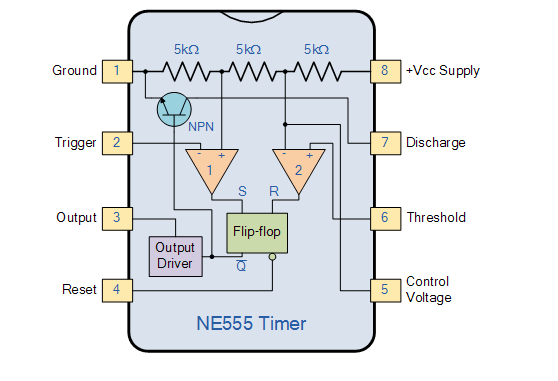
• Pin No. 1 – Ground,
• Pin 2. – Trigger, The negative input to comparator No 1. The ground pin links the 555 timer to the negative (0v) supply rail. When the voltage dips below 1/3Vcc, a negative pulse on this pin “sets” the internal Flip-flop, causing the output to go from a “LOW” to a “HIGH” state. Small speakers, LEDs, and motors can be connected directly to the output pin, which can drive any TTL circuit and source or sink up to 200mA of current at an output voltage of about Vcc - 1.5V.
• Pin 4 – Resets the device. This pin is utilised to “reset” the internal Flip-flop that controls the output state, pin 3. When not in use, this is an active-low input that is usually connected to a logic "1" level to prevent the output from being reset.
• Pin 5 – Voltage Control This pin overrides the voltage divider network's 2/3Vcc level to control the 555's timing. The width of the output signal can be changed independently of the RC timing network by supplying a voltage to this pin. To avoid noise, it is connected to ground through a 10nF capacitor while not in use.
• Pin 6 – Threshold, the comparator No 2's positive input. When the voltage supplied to this pin exceeds 2/3Vcc, the Flip-flop is reset, causing the output to transition from “HIGH” to “LOW.” This pin links to the RC timing circuit directly.
• Pin 7. – Discharge, When the output at pin 3 switches “LOW,” the discharge pin is connected directly to the Collector of an internal NPN transistor, which is used to “discharge” the timing capacitor to ground.
• Pin 8 – Supply +Vcc, This is the power supply pin, which is between 4.5V and 15V for general purpose TTL 555 timers.