Unit - 1
Semiconductor Diodes
Q1) Discuss electrostatic relationship for step junction for VA = 0?
A1)
Electrostatic Relationships
The development of quantitative relationships for the electrostatic variables deals with the step junction and is presented in detail not only to obtain the desired relationships but also to establish the derivational procedures that can be applied to other doping profiles.
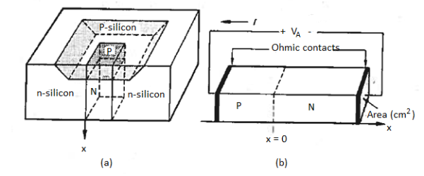
Figure 1: (a) Sketch of o physical diode. (b) One-dimensional diode subjected to the applied voltage, coordinates, and contact specifications.
Assumptions
Major features of the pn junction diode subject to analysis are identified in Figure 1.
- All variables are taken to be functions only of x, the coordinate normal to the semiconductor surface.
- The device is thus said to be "one-dimensional"; obvious two-dimensional effects associated with the lateral ends of a real device are assumed to be negligible.
- For the electrostatic analysis, x = 0 is positioned at the metallurgical boundary.
- External contacts to the ends of the diode are specified to be "ohmic" in nature.
- By definition, a negligible portion of an externally applied voltage appears across an ohmic contact.
- Symbol VA is used for the applied voltage. The subscript A distinguishes the applied voltage from the internal junction voltage.
- In the initial development VA is set equal to zero, or equivalently, the device is assumed to be in equilibrium.
Step Junction with VA = 0
Solution for ρ
We consider a step junction under equilibrium conditions. NA is drawn greater than ND in the Figure 1(a) sketch of the doping profile for the sake of illustration. As summarized in Figure 1(b), invoking the depletion approximation yields the charge density solution
 ……….(1)
The values of xn and xp are not known at this point but will be determined later in the analysis.
Solution for ξ
Substituting the charge density solution into Poisson's equation gives the equations to be solved for the electric field.
 ……….(2)
ξ = 0 far from the metallurgical boundary and therefore ξ = 0 everywhere outside of the depletion region. Since must also vanish right at the edges of the depletion region, ξ = 0 at x = — xp and ξ = 0 at x = xn respectively become the boundary conditions for the differential equations (1).
Separating variables and integrating from the depletion region edge to an arbitrary point x, one obtains for the p-side of the depletion region
 ……….(3)
 ……….(4)
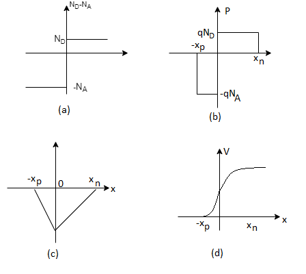
Figure 2: Step Junction solution. Depletion approximation based quantitative solution for the electrostatic variables in pn step junction at equilibrium condition (VA= 0) (a) Step junctions profile. (b) Charge density, (c) electric field, and (d) electric potential as a function of position x.
Similarly for the n-side
 ……….(5)
 ……….(6)
The electric field solution is plotted in Figure 2(c). It is clear that
- Within the depletion region the field is always negative and exhibits a linear variation with position.
- The electric field was taken to be continuous at x = 0; the p- and n-side solutions were simply matched at the metallurgical boundary.
From Electricity and Magnetism, we know the electric field will be continuous across a boundary as long as a sheet of charge does not lie along the interface between the two regions. If the equations (4) and (6) expressions for the electric field are evaluated at x = 0 and equated, the continuity of the electric field is found to require
NAXp = NDXn ……….(7)
For those familiar with Gauss' law, the fact that ξ = 0 outside the depletion region means the total charge within the depletion region must sum to zero, or the minus charge on the p-side of the junction must balance the plus charge on the n-side of the junction.
Applied to the step junction ρ versus x plot in Figure 2(b), the balance of charge requires the rectangular areas on the p- and n-sides of the junction to be equal, or (qNAXp = qNDXn)
Thus Equation (7) gives the fact that the total charge within the depletion region must sum to zero.
Solution for V
Since ξ = — dV/dx, the electrostatic potential is obtained by solving
 …….(8)
With the arbitrary reference potential set equal to zero at x = —xp, and remembering the voltage drop is Vbi across the depletion region under equilibrium conditions, Equation (8) are respectively subject to the boundary conditions given as

 ……….(9)
Separating variables and integrating from the depletion region edge to an arbitrary point x, one obtains for the p-side of the depletion region
 ……….(10)
 ……….(11)
For n side
 ……….(12)
 ……….(13)
The electrostatic potential solution given by Equations (11) and (13) is plotted in Figure 2(d). The V versus x dependence is quadratic in nature, with a concave curvature on the p-side of the junction and a convex curvature on the n-side of the junction.
Paralleling the ξ -field procedure, Fig. 5.9(d) was constructed simply by matching the p- and n-side solutions at x = 0. The assumed continuity of the electrostatic potential at x = 0 is justified because there is no dipole layer (closely spaced sheets of plus and minus charge) along the metallurgical boundary.
The Equations (11) and (13) expressions for the potential are evaluated at x =0 and equated, one obtains
 …………(14)
Solution for xp and xn
The electrostatic solution is not complete until the values of xp and xn are determined. Specifically, xp and xn are the only unknowns in Equations (7) and (14). Using (7) in (14) we can found xn.
 …………(15)
And after solving further the value of xp comes to be
 …………(16)
Thus we get
 …………(17)
W is the total width of the depletion region, better known simply as the depletion width.
Q2) Discuss electrostatic relationship for step junction for VA  0 and VA
  0?
0?
A2)
Step Junction with VA 
For the practical purpose the solution for the electrostatic variables must be extended to VA  .
.
Consider the diode in Figure 3 with a voltage VA  applied to the diode terminals. This voltage must be dropped somewhere inside the diode. However, in a well-made device a negligible portion of the applied voltage appears across the contacts to the device.
More-over, under low-level injection conditions (reasonable current levels) the resistive voltage drop across the quasi-neutral p- and n-regions extending from the contacts to the edges of the depletion region will also be negligible.
The applied voltage must therefore be dropped across the depletion region. When VA> 0. This externally imposed voltage drop lowers the potential on the n-side of the junction relative to the p-side of die junction. Conversely, when VA < 0, the potential on the n-side increases relative to the p-side.
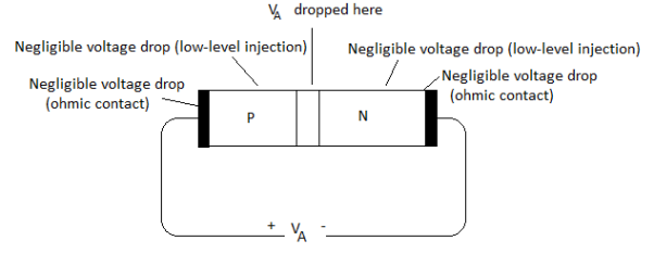
Figure 3: Voltage drops internal to a diode resulting from external applied voltage.
In other words, the voltage drop across the depletion region, and hence the boundary condition at x = xn, becomes Vbi - VA.
Since the only modification to the formation of the problem is a change in one boundary condition, the VA  electrostatic relationships can be extrapolated from the VA = 0 relationships by simply replacing all explicit appearances of Vbi by Vbi - VA.
Making the indicated substitution yields the VA  solution for the electrostatic variables given in Equations.
For -xp  x
x 0
0
 …………(18)
 …………(19)
 …………(20)
For  x
x xn
xn
 …………(21)
 …………(22)
 …………(23)
Thus depletion width become
 …………(24)
To prevent so imaginary result, VA is obviously restricted to VA  Vbi in Equations (20), (23) and (24). The formulation fails because a large current begins to flow, and quasineutral region voltage drops cannot he neglected, when VA approaches Vbi.
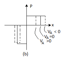
Let us see how the electrostatic variables change as a function of the applied bias. Examining the (20) and (23) relationships for xp and xn, we conclude these widths decrease under forward biasing (VA > 0) and increase under reverse biasing ( VA < 0).
The changes in xp and xn likewise translate into changes in the electric field. As deduced from Equations (18) and (21), a smaller xp and xn under forward biases cause the ξ -field to decrease everywhere inside the depletion region while-the larger xp and xn associated with reverse biases give rise to a larger ξ -field.
This conclusion is also reasonable from a physical standpoint. A decreased depletion width when VA > 0 means less charge around the junction and a correspondingly smaller ξ-field. On the other hand VA<0, creates a larger space charge region and a bigger electric field,
The potential given by Equations (19) and (22) decreases at all points when VA > 0 and increases at all points when VA < 0. The potential hill shrinks in both size and x-extent under forward biasing, whereas reverse biasing gives rise to a wider and higher potential hill.
This is summarized graphically in figure 4.
 |  |
 | 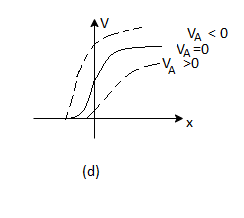 |
Figure 4: Effect of forward and reverse biasing on the (a) depletion width, (b) charge density (c) electric field and (d) electric potential inside a pn junction diode.
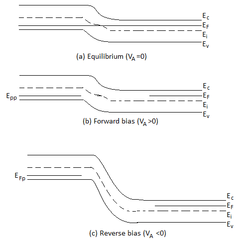
Figure 5: pn junction energy band diagrams. (a) Equilibrium (VA = 0), (b) forward bias (VA>0), and (c) reverse bias (VA< 0).
We come across that the energy band diagram under equilibrium condition. Conceptually taking the upside-down of the potential plots and appropriately modifying the equilibrium energy band diagram—smaller depletion width and smaller hill for forward bias, larger depletion width and larger hill for reverse bias—yields the diagrams for forward and reverse bias respectively pictured in Figure (b) and (c).
From figure it is clear the Fermi level is omitted from the depletion region because the device is no longer in equilibrium and a single level cannot be used to describe the carrier concentrations in this region. In fact, the levels labelled EFn and EFp occupying the former position of the Fermi level in the quasineutral regions, are actually majority-carrier quasi-Fermi levels.
However, the deviation from equilibrium in the non-depleted portions of the diode is normally small, especially far from the junction, and it is therefore acceptable to continue using the EF designation.
EFp - EFn = qVA
Q3) Discuss Depletion Width?
A3)
Depletion Width
Depletion region or depletion layer is a region in a P-N junction diode where no mobile charge carriers are present. Depletion layer acts like a barrier that opposes the flow of electrons from n-side and holes from p-side.
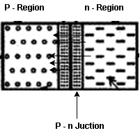
Figure 6: Depletion region
At the instant of junction formation, free electrons in the N-region near the p-n junction being to diffuse across the junction and fall into holes near the junction in the P-region. The width of depletion region depends on the amount of impurities added to the semiconductor.
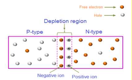
Figure 7: Depletion region
The Depletion region acts as a barriers to the farther movement of electrons across the junction
As positive ion & -ve ion across the junction produces a electric field across the junction -according to coulombs law.
The potential difference of the electric field across the depletion region is the amount of voltage required to move electronics through the electric field, this potential difference is called the barrier potential & is expressed in volt
The typical barrier potential is approximately 0.7 v for silicon & 0.3 v for germanium at 25c.
Depletion width of two sided abrupt junction can be calculated by the following formula

For one sided abrupt junction it is given by the following formula

Q4) What is Drift current and diffusion currents? Derive expression for total hole and total electron current?
A4)
In case of semiconductors we observe two kinds of currents.
- Drift current
- Diffusion current
Drift current Definition: The flow of electric current due to the motion of charge carriers under the influence of external electric field is called drift current.
When an electric field E is applied across a semiconductor material, the charge carriers attain a drift velocity vd
So drift velocity vd =μ .E
The relation between current density J and drift velocity vd is
J = Nqvd
Where N is the carrier concentration
q is the charge of electron or hole
From equations (1) and (2), we get
Jdrift = Nq μE
μ is the mobility of charge carrier.
The above equation shows the general expression for drift current density. Drift current density due to electrons is
Je(drift) = neμeE
Where n is the electrons carrier concentration
And μe is the mobility of electrons.
Drift current density due to holes is
Jh(drift) = peμhE
Where p is the carrier concentration of holes.
μh is the mobility of holes
So Total drift current density
Jdrift (total) = Je(drift) + Jh(drift) = neμeE + peμhE
= eE (nμe+pμh )
Diffusion current
Definition:-The flow of electric current due to the motion of charge carriers under concentration gradient is called diffusion current
Or
The motion of charge carriers from the region of higher concentration to lower concentration leads to a current called diffusion current.
Let ∆N be the excess electron concentration. Then according to Fick’s law, the rate of diffusion of charge carriers is proportional to concentration gradient
Rate of diffusion of charge ∝ -
= - D
Where D is the diffusion coefficient of charge carriers.
The negative sign indicates decrease of N with increase of x So,
The diffusion current density Jdiffu is
Jdiffu = - qD
Where q is the charge of the charge carrier
Diffusion current density due to holes is
Jdiffu (hole) = - eDh
Diffusion current density due to electrons is (as electron carry negative charge so we will get +sign here.
Jdiffu (electrons) = eDe
Jdiffu (total) = Jdiffu (hole) + Jdiffu (electrons)
Jdiffu (total) = - eDh + eDe
+ eDe
The expression for total current density due to holes is
Jh (total) = Jh(drift) + Jdiffu (hole) = peμhE - eDh
The expression for total current density due to electrons is
Je (total) = Je(drift) + Jdiffu (electrons) = neμeE + eDe
Q5) Write a note on carriers?
A5)
We already know that that there are no carriers or possible current flow if the bonding model has no broken bonds. Equivalently, in the energy band model, if the valence band is completely filled with electrons and the conduction band is devoid of electrons. There are no carriers or possible current flow. This lack of carriers and associated current flow is easy to understand in terms of the bonding model where the shared electrons are viewed as being tied to the atomic cores.
As accurately portrayed in the energy band model, however, the valence band electrons actually move about in the crystal. How is it then that no current can arise from this group of electrons? As it turns out, the momentum of the electrons is quantized in addition to their energy. Moreover, for each and every possible momentum state in a band, there is another state with an oppositely directed momentum of equal magnitude. Thus, if a band is completely filled with electrons, the net momentum of the electrons in the band is always identically zero. It follows that no current can arise from the electrons in a completely filled energy band.
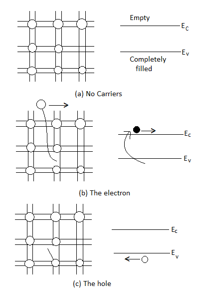
Figure 8: Visualization of carriers using the bonding model (left) and the energy band model (left) (a) No-carrier situation (b) Visualization of electrons (c) Visualization of hole.
The electrons that do give rise to charge transport are visualized in Figure above. When a Si—Si bond is broken and the associated electron is free to wander about the lattice, the released electron is a carrier. Equivalently, in terms of the energy band model, excitation of valence band electrons into the conduction band creates carriers; that is, electrons in the conduction band are carriers.
Note that the energy required to break a bond in the bonding model and the band gap energy are one and the same thing. Likewise. Freed bonding-model electrons and conduction band electrons are just different names for the same electrons.
In addition to releasing an electron the breaking of a Si-Si bond also creates a missing bond or void in the bonding structure.
By bonding modelled one can visualize the movement of this missing bond from place to place in the lattice as a result of nearby bound electrons jumping into the void
By the energy band model one can visualize the removal of an electron from the valence band creates an empty state in vast sea of filled stales. The empty slate in the valence band. Is the second type of carnet found in semi-conductors—the hole. Both electrons and holes participates in the operation of most semiconductor devices.
Q6) Write a note on mobility?
A6)
The drift velocity produced per unit electric field is called 'mobility' , Thus Mobility is obviously a central parameter in characterizing electron and hole transport due to drift.
μ =  or μE =
The word mobility refers to freedom of movement. Analogously, in semiconductor work the mobility parameter is a measure of the ease of carrier motion in a crystal. Increasing the motion-impeding collisions within a crystal decreases the mobility of the carriers.
In other words, the carrier mobility varies inversely with the amount of scattering taking place within the semiconductor.
Lattice scattering involving collisions with thermally agitated lattice atoms, and ionized impurity (i.e., donor-site and/or acceptor-site) scattering. Relative to lattice scattering, it should be emphasized that it is the thermal vibration, the displacement of lattice atoms from their lattice, positions, that leads to carrier scattering. The internal field associated with the stationary array of atoms in a crystal is already taken into account in the effective mass formulation.
μ = q /m*
/m*
Where  is the mean free time between collisions and m* is the conductivity effective mass.
However, μ is also noted to vary inversely with the carrier effective mass—lighter carriers move more readily.
The carrier mobilities are essentially independent of the doping concentration. For dopings in excess of l015/cm3, the mobilities monotonically decrease with increasing NA or ND.
The mobilities of carrier depend upon temperature as μ 
 . For Electrons μe
 and for holes μp

Q7) Write a note on the concept of drift?
A7)
Drift is charged-particle motion in response to an applied electric field.
Within semiconductors the drifting motion of the carriers on a microscopic scale can be described as follows: When an electric field (Si) is applied across a semiconductor as visualized in figure (a) the resulting force on the carriers tends to accelerate the +q charged holes in the direction of the electric field and the — q charged electrons in the direction opposite to the electric field. Because of collisions with ionized impurity atoms and thermally agitated lattice atoms, however, the carrier acceleration is frequently interrupted (the carriers are d to be scattered). The net result, pictured in Figure (b), is carrier motion generally along the direction of the electric field, but in a disjointed fashion involving repeated periods of acceleration and subsequent decelerating collisions.

Figure 9: Visualization of carrier drift: (a) motion of carriers within a biased semiconductor bar (b) drifting hole on microscopic or atomic state (c) carrier drift on a macroscopic state.
The microscopic drifting motion of a single carrier is difficult to analyse as it is complex however the measurable quantities are macroscopic observables that gives the average or overall motion of the carriers.
Averaging over all electrons or holes at any given time, we find that the resultant motion of each carrier type can be described in terms of a constant drift velocity, vd
In other words, on a macroscopic scale, drift may be visualized as nothing more than all carriers of a given type moving along at a constant velocity in a direction parallel or antiparallel to the applied electric field.
It is important to point out that the drifting motion of the carriers arising in response to an applied electric field is actually superimposed upon the always-present thermal motion of the carriers. Electrons in the conduction band and holes in the valence band gain and lose energy via collisions with the semiconductor lattice and are nowhere near stationary even under equilibrium conditions. In fact under equilibrium conditions the thermally related carrier velocities average  1/1000 the speed of light at room temperature.
However, the thermal motion of the carriers is completely random. Thermal motion therefore averages out to zero on a macroscopic scale, does not contribute to current transport, and can be conceptually neglected.
Q8) Discuss Half Wave Rectifier?
A8)
- It is the simplest form of the rectifier. Here, a single diode is used.
- It consists of an AC source, transformer (step-down), diode, and resistor (load).
- The diode is placed between the transformer and resistor (load).
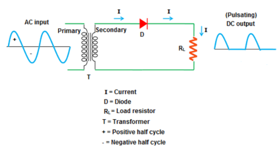
Figure 10: Half Wave Rectifier
Operation:
- It allows only half cycle and blocks the other half cycle.
- When it allows positive half cycles and blocks negative half cycles, it is called a positive half wave rectifier. The output DC current or DC signal produced by a positive half wave rectifier is a series of positive half cycles or positive sinusoidal pulses.
- When it allows electric current during the negative half-cycle of input AC signal and blocks electric current during the positive half-cycle of the input AC signal.
- A negative half wave rectifier produces a series of negative sinusoidal pulses.
- For an ideal diode, the positive half cycle or negative half cycle at the output is exactly same.
Characteristics of half wave rectifier
Ripple factor
The ripple factor is given as

Finally, we get
γ = 1.21
Hence, the DC voltage is 121% of the DC magnitude.
DC current
The DC current is given by,

Where,
Imax = maximum DC load current
Output DC voltage (VDC)
The output DC voltage is given by,

Where, VSmax = Maximum secondary voltage
Rectifier efficiency
It is defined as the ratio of output DC power to the input AC power.
The rectifier efficiency of a half wave rectifier is 40.6%
Root mean square (RMS)
The root mean square (RMS) value of load current in a half wave rectifier is

The root mean square (RMS) value of output load voltage in a half wave rectifier is

Form factor
It is defined as the ratio of RMS value to the DC value given by,
F.F = RMS value / DC value
The form factor of a half wave rectifier is F.F = 1.57
Advantages:
- Very few components are used. So, the cost is very low.
- Easy to construct
Disadvantages:
- Loss of power
- Pulsating direct current
- Produces low output voltage.
Q9) A half-wave rectifier is used to supply 50V d.c. To a resistive load of 800 Ω. The diode has a resistance of 25 Ω. Calculate a.c. Voltage required.
A9)
Output d.c. Voltage 
Diode resistance 
Load resistance 
Let  be the maximum value of a.c. Voltage required


Hence a.c. Voltage of maximum value 162 V is required
Q10) Discuss Centred-taped and Bridge Wave Rectifier?
A10)
Full Wave Rectification
Types on the basis of construction:
- Center-taped transformer
It consists of two power diodes connected to a single load resistance (RL) and each diode supply current to the load one by one. When point A of the transformer becomes positive, diode D1 conducts in the forward direction.
When point B becomes positive (for the negative half of the cycle) with respect to point C, diode D2 conducts and the current starts flowing through resistor R is in the same direction for both half-cycles.
As the output voltage across the resistor R is the sum of the two waveforms combined, this type of circuit is also called as a “bi-phase” circuit.
The spaces present between the frequency response of each half-wave developed by each diode is now being filled in by the other therefore, the average DC output voltage across the load resistor becomes double that of the single half-wave rectifier circuit.
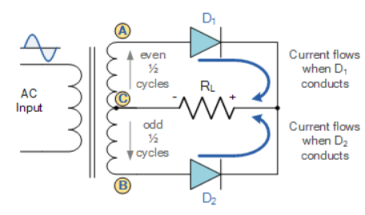
Figure 11: Center-taped
2. Bridge Rectifier
It uses four individual rectifying diodes which are connected in a closed loop called “bridge” configuration to produce the desired output.
It does not require a special centre tapped transformer, hence reducing its size and cost. The single secondary winding is connected one side to the diode bridge network and the other side to the load.
The four diodes D1 to D4 are arranged in “series pairs” and only two diodes conduct current during each half cycle.
During the positive half cycle, diodes D1 and D2 conduct in series while diodes D3 and D4 are reverse biased producing current through the load.
During the negative half cycle, diodes D3 and D4 conduct in series and diodes D1 and D2 are switched “OFF” as they become reverse biased producing current through the load.
During each half cycle the current flows through two diodes instead of just one. The ripple frequency is now twice the supply frequency.
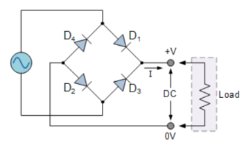
Figure 12: Bridge Rectifier
Output Waveform:
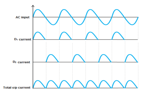
Figure 13: Output Waveform
Q11) Discuss Characteristics of full wave rectifier?
A11)
Characteristics of full wave rectifier
Ripple factor
The ripple factor is given by

Finally, we get γ = 0.48
Rectifier efficiency
It is defined as the ratio of DC output power to the AC input power.
It can be mathematically written as
η = output PDC / input PAC
The rectifier efficiency of a full wave rectifier is 81.2%.
Peak inverse voltage (PIV)
It is the maximum voltage a diode can withstand in the reverse bias condition.
The peak inverse voltage (PIV) = 2Vsmax
DC output current
The current produced by D1 is Imax / π and the current produced by D2 is Imax / π.
So, the output current IDC = 2Imax / π
Where, Imax = maximum DC load current
DC output voltage
The DC output voltage appeared at the load resistor RL is given as
VDC = 2Vmax /π
Where,
Vmax = maximum secondary voltage
Root mean square (RMS) value of load current IRMS
The root mean square (RMS) value of load current in a full wave rectifier is

The root mean square (RMS) value of output load voltage in a full wave rectifier is

Form factor
It is the ratio of RMS value of current to the DC output current
F.F = RMS value of current / DC output current
The form factor of a full wave rectifier is F.F = 1.11
Advantages:
- High rectifier efficiency
- Low power loss
- Low ripples
- It has fewer ripples than the half wave rectifier.
Disadvantages:
- High cost
- The center tapped transformers are expensive and occupy a large space.
Q12) A full-wave rectifier uses two diodes, the internal resistance of each diode may be assumed constant at 20 Ω. The transformer r.m.s. Secondary voltage from center tap to each end of secondary is 50 V and load resistance is 980 Ω. Find: (i) the mean load current (ii) the r.m.s. Value of load current.
A12)

Max a.c. Voltage 
Max. Load current 
(i) Mean load current 
(ii) R.M.S value of load current is

Q13) Discuss Zener diode?
A13)
The satisfactory explanation of this breakdown of the junction was first given by the American scientist C. Zener. A zener diode is a special type of diode that is designed to operate in the reverse breakdown region.
An ordinary diode operated in this region will usually be destroyed due to excessive current. This is not the case for the zener diode.
It has already been discussed that when the reverse bias on a crystal diode is increased, a critical voltage, called breakdown voltage is reached where the reverse current increases sharply to a high value. The breakdown region is the knee of the reverse characteristic as shown in Figure.
The breakdown voltage is sometimes called zener voltage and the sudden increase in current is known as zener current.
The breakdown or zener voltage depends upon the amount of doping. If the diode is heavily doped, depletion layer will be thin and consequently the breakdown of the junction will occur at a lower reverse voltage.
On the other hand, a lightly doped diode has a higher breakdown voltage. When an ordinary crystal diode is properly doped so that it has a sharp breakdown voltage, it is called a zener diode. A properly doped crystal diode which has a sharp breakdown voltage is known as a zener diode.
Figure shows the symbol of a zener diode. It may be seen that it is just like an ordinal, diode except that the bar is turned into z-shape.
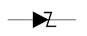
Figure 14: Symbol of a Zener diode
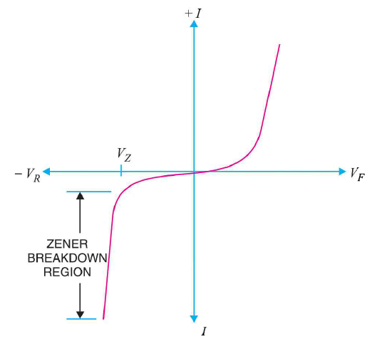
Figure 15: I-V characteristics of zener diode
As the curve reveals, two things happen when Vz is reached:
- The diode current increases rapidly.
- The reverse voltage Vz across the diode remains almost constant.
The following points may be noted
(i) A zener diode is like an ordinary diode except that it is properly doped so as to have a sharp breakdown voltage.
(ii) A zener diode is always reverse connected i.e. it is always reverse biased.
(iii) A zener diode has sharp breakdown voltage, called zener voltage Vz.
(iv) When forward biased, its characteristics are just those of ordinary PN junction diode.
(v) The zener diode is not immediately burnt just because it has entered the breakdown region. As long as the external circuit connected to the diode limits the diode current to less than burn out value, the diode will not burn out.
In other words, the zener diode operated in this region will have a relatively constant voltage across it, regardless of the value of current through the device. This permits the zener diode to be used as a voltage regulator or voltage stabiliser.
- Zener diode is a special type of p-n junction semiconductor diode. In this diode, the reverse breakdown voltage is adjusted precisely between 3 V to 200 V.
- Its applications are based on this principle hence Zener diode is called as a breakdown diode.
- The doping level of the imparity added to manufacture the Zener diode is controlled in order to adjust the precise value of breakdown voltage.
Q14) Discuss Zener diode operation and its application in voltage regulation?
A14)
Principle of Operation:
A Zener diode can be forward biased or reverses biased. Its operation in the forward biased mode is same as that of a p-n junction diode but its operation in the reverse biased mode is sustainably different.

Figure 16: Zener diode
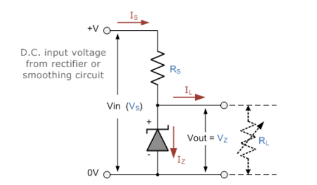
Figure 17: Zener diode
- The resistor, RS is connected in series with the Zener diode to limit the current flow through the diode with the voltage source, VS being connected across the combination. The stabilised output voltage Vout is taken from across the Zener diode.
- The Zener diode is connected with its cathode terminal connected to the positive rail of the DC supply so it is reverse biased and will be operating in its breakdown condition. Resistor RS is selected so to limit the maximum current flowing in the circuit.
- The load is connected in parallel with the Zener diode, so the voltage across RL is always the same as the Zener voltage, (VR = VZ).
- There is a minimum Zener current for which the stabilisation of the voltage is effective, and the Zener current must stay within the value operating under load within its breakdown region at all times.
- The upper limit of current is of course dependent upon the power rating of the device. The supply voltage VS must be greater than VZ.
- A Zener diode is always operated in its reverse biased condition. As such a simple voltage regulator circuit can be designed using a Zener diode to maintain a constant DC output voltage across the load despite variations in the input voltage or changes in the load current.
- The Zener voltage regulator consists of a current limiting resistor RS connected in series with the input voltage VS with the Zener diode connected in parallel with the load RL in this reverse biased condition.
- The stabilised output voltage is always selected to be the same as the breakdown voltage VZ of the diode.
Voltage Regulators
They are used more due to less cost and are effective. Zener diode is used for voltage regulation in the circuit. At maximum load current the shunt regulator draws virtually no current and at minimum load current, the shunt voltage regulator passes the full current. Zener diode a shunt regulator is shown below.
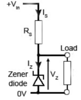
Figure 18: Voltage Regulators
There is voltage drop across the resistor in series to the source. The voltage across the Zener diode is maintained irrespective of the change in current. It takes up the current variations required to ensure the correct drop across the series resistor. In this way it shunts sufficient current to maintain the voltage across its terminals and hence the load.
It is an open loop connection. Shunt voltage regulators are not particularly effective or efficient in high current situations. The simple Zener diode voltage regulator, when used as a low current voltage reference is widely used, and its inefficiency can be tolerated in view of the low current.
Q15) A 5.0V stabilised power supply is required to be produced from a 12V DC power supply input source. The maximum power rating PZ of the Zener diode is 2W. Using the Zener regulator circuit above calculate:
a). The maximum current flowing through the Zener diode.
b). The minimum value of the series resistor, RS
c). The load current IL if a load resistor of 1kΩ is connected across the Zener diode.
d). The Zener current IZ at full load.
A15)
a). The maximum current flowing through the Zener diode.
Maximum current = Watts/ Voltage = 2w/ 5V = 400mA
b). The minimum value of the series resistor, RS
Rs = Vs – Vz/ Iz = 2 – 5 / 400mA = 17.5 Ω
c). The load current IL if a load resistor of 1kΩ is connected across the Zener diode.
IL = Vz / RL = 5v/ 1000Ω = 5mA
d). The Zener current IZ at full load.
IZ = Is – IL = 400 mA – 5mA = 395mA
Q16) Explain LED Laser?
A16)
LED or Light emitting diode
Light emitting diode is a pn junction device. It is always operated in forward biased condition. LED converts electrical energy into light energy.
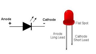
Figure 19: LED
Device Structure:
The LED structure plays a crucial role in emitting light from the LED surface. The LEDs are structured to ensure most of the recombination takes place on the surface by the following two ways.
- By increasing the doping concentration of the substrate, so that additional free minority charge carriers electrons move to the top, recombine and emit light at the surface.
- By increasing the diffusion length L =√Dτ, where D is the diffusion coefficient and τ is the carrier life time.
But when increased beyond a critical length there is a chance of reabsorption of the photons into the device. The LED has to be structured so that the photons generated from the device are emitted without being reabsorbed.
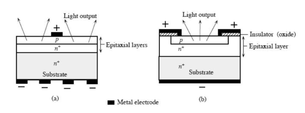
Figure 20: A schematic illustration of typical planar surface emitting LED devices. (a) p-layer grown epitaxially on an n+ substrate. (b) First n+ is epitaxially grown and then p region is formed by dopant diffusion into the epitaxial layer.
One solution is to make the p layer on the top thin, enough to create a depletion layer. Following picture shows the layered structure. There are different ways to structure the dome for efficient emitting
LEDs are usually built on an n-type substrate, with an electrode attached to the p-type layer deposited on its surface. P-type substrates, while less common, occur as well. Many commercial LEDs, especially GaN/InGaN, also use sapphire substrate.
In the fabrication of LED’s direct band gap semiconductors like GaP, GaAsP are used. In direct band gap semiconductors most of the energy is emitted in the form of light when hole and electron recombination takes place.
When an LED is forward biased the electrons and holes move in towards the junction and recombination takes place. As a result of recombination the electrons lying in the conduction band of an n- region fall into the holes lying in the valence band of a p –region. The difference of energy in the valence band and conduction band is radiated in the form of light energy. Here their excess energy is transferred to the emitted photon. The brightness of emitted light is directly proportional to the forward bias current.
Figures of Merit
A very important metric of an LED is the external quantum efficiency ηext. It quantifies the efficiency of the conversion of electrical energy into emitted optical energy.
Not all the photons emitted from the active region of an LED make it out of the device. Some are reabsorbed, some go in the wrong direction, some are reflected back. The light extraction efficiency of a LED is,
ηextraction 
The external quantum efficiency ext of a LED is,
ηextraction 
It is defined as the light output divided by the electrical input power. It is also defined as the product of Internal radiative efficiency and Extraction efficiency. ηext = Pout(optical) / IV
For indirect bandgap semiconductors ηext is generally less than 1%, whereas for a direct band gap material it could be substantial.
ηint = rate of radiation recombination/ Total recombination
The internal efficiency is a function of the quality of the material and the structure and composition of the layer.
LED materials
LEDs are comprised of compound semiconductor materials, which are made up of elements from group III and group V of the periodic table (these are known as III-V materials). Examples of III-V materials commonly used to make LEDs are gallium arsenide (GaAs) and gallium phosphide (GaP).
Ternary alloys based on alloying GaAs and GaP which are denoted by GaAs1-yPy. InGaAlP is an example of a quarternary (four elements) III-V alloy with a direct band gap. The LEDs realized using two differently doped semiconductors that are the same material is called a homojunction. When they are realized using different bandgap materials they are called a heterostructure device. A heterostructure LED is brighter than a homoJunction LED.
The main semiconductor materials used to manufacture LEDs are:
- Indium gallium nitride (InGaN): blue, green and ultraviolet high-brightness LEDs
- Aluminum gallium indium phosphide (AlGaInP): yellow, orange and red high-brightness LEDs
- Aluminum gallium arsenide (AlGaAs): red and infrared LEDs
- Gallium phosphide (GaP): yellow and green LEDs
Characteristics of LED
LEDs are solid-state devices. The advantages are:
1) Light Generated by LED is Directional
2) LED can Generate Different Light Color
3) Temperature will Affect LED Efficacy
4) Low Energy Consumption
5) Long Life
The usage of LED is advantageous as it consumes less power and produces less heat. LEDs last longer than incandescent lamps.
Applications LEDs are used in
- For instrument display
- In calculators
- Digital clocks
- For indicating power ON/ OFF
- For optical switching application
- In optical communication system
- Medical devices
Q17) Write a note on Solar cell?
A17)
Solar Cells
A solar cell or photo-voltaic cell is an electronic device that directly converts sun’s energy into electricity. When sunlight falls on a solar cell, it produces both a current and a voltage to produce electric power.
Sunlight, which is composed of photons, radiates from the sun. When photons hit the silicon atoms of the solar cell, they transfer their energy to lose electrons; and then, these high-energy electron flow to an external circuit.
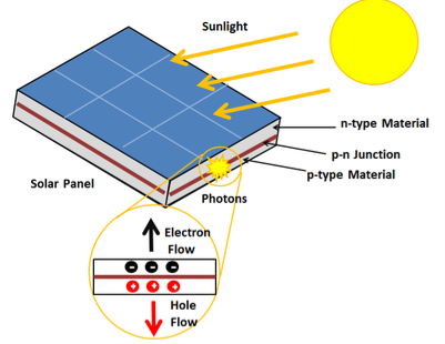
Figure 21: Solar Cell
The solar cell is composed of two layers which are struck together. The first layer is loaded with electrons, so these electrons are ready to jump from the first layer to the second layer. The second layer has some electrons taken away, and therefore, it is ready to take more electrons.
The advantages of solar cells are that, there is no fuel supply and cost problem. These are very dependable and require little maintenance.
A key issue with solar cells is conversion efficiency—convening the maximum amount of available solar energy into electrical energy. The higher the efficiency of the cells, the lower the cost and collection area required to achieve a desired electrical output.
A number of factors enter into the overall efficiency exhibited by a cell and involve both material and design considerations. Any discussion of conversion efficiency logically begins with the output from the sun.
Given a specific semiconductor material, it is the task to design and fabricate the solar cell to minimize further energy losses. In discussing device-related loss mechanisms, we will refer to the high-efficiency Si solar cell pictured in Figure.
Observe first of all that the contact to the top (light-incident) side of the cell is made through narrow "fingers." The fingers, all connected together along one edge of the cell are a design compromise. Zero-width fingers or fingers only along the cell edges would allow maximum light penetration to the underlying silicon. However, a series resistance of only a few ohms can seriously degrade the efficiency of a solar cell. The farther apart the fingers, the longer the current path through the narrow n-region at the top of the cell, and the greater the series resistance. Metallization and contact resistances can become important if the fingers are too narrow. The chosen finger size and spacing are calculated to provide an optimum trade-off between residual "shadowing," blocking of some of the light that strikes the cell, and cell series resistance.
Another potentially significant loss mechanism is the reflection of light at the Si surface. Approximately 30% of the light striking a bare planar Si surface at normal incidence will be reflected. To minimize losses due to reflection, the top surface of solar cells are typically "textured" and covered with an antireflection coating. Texturing of the surface, the formation of the inverted pyramids in decreases the reflected light by forcing the light to strike the Si surface two or more times before escaping.
Texturing is achieved by placing the Si in an anisotropic etching solution, an etch that preferentially removes Si atoms along certain crystalline planes. Having an index of refraction intermediate between air and Si, the top SiO2 layer in the pictured cell, or preferably a deposited antireflection coating with optimized parameters, further reduces the reflection.
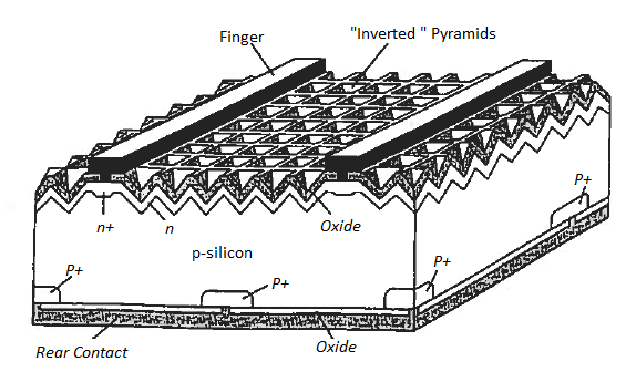
Figure 22: Solar Cell
Solar cells constructed in the described manner have attained a net reflection of less than 1%. Once the light has entered the semiconductor, the focus shifts to maximizing the light absorption.
In the Figure solar cell the bottom surface oxide and metallization effectively form a mirror that reflects light hack into the silicon. Long wavelength light literally 1 bounces back and forth between the top and bottom surfaces of the cell. This "light trap-ping" dramatically enhances the long (λ— λG) wavelength absorption.
Finally, the cell must be designed and built to collect as many of the photogenerated minority carriers as possible. This necessitates minimizing carrier recombination through-out the device structure.
Very long minority carrier lifetimes are the rule in modern single-crystal Si cells, yielding diffusion lengths greater than the width of the cell. With the top and bottom surfaces also carefully oxidized to minimize surface recombination, carriers generated almost anywhere in the cell volume have a high probability of diffusing to the depletion region and being swept to the opposite side of the junction before they recombine.
Q18) What do you mean by FF or fill factor?
A18)
Solar Cell Basics
A variety of device structures have been employed in constructing solar cells. By far and away the most common cells are in essence just large-area pn junction photodiodes. Solar cells are designed of course to minimize energy losses, whereas photodiodes arc routinely designed to achieve a specific spectral response or a rapid time response.
Although there is design differences but I—V characteristics of solar cell are of the same general form as the photodiode characteristics.
We know that power is derived from the illuminated device if the d.c. Operating point lies in the fourth quadrant where I is negative and V is positive. Fourth-quadrant operation can be achieved in case of solar cell just by simply placing a resistor in series with the illuminated solar cell.
The fourth-quadrant characteristic is of prime interest in evaluating and applying solar cells. It is therefore common practice to show only the fourth-quadrant portion of the characteristics and to orient the — I axis upward on the plot as illustrated in Figure.
Figure also graphically defines the following solar cell parameters of interest:
Voc - the open circuit voltage
Isc - the short circuit current
Vm Im - the operating point voltage and current yielding the maximum power output.
Voc is obviously the maximum voltage that can be supplied by the cell for a given photoinput,
Is, is the maximum current that can be derived from the cell.
It follows that Pmax = Vm Im < Voc Isc
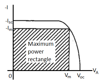
Figure 23: Inserted fourth-quadrant I—V characteristic of a solar cell under illumination with key solar cell parameters identified along the coordinate axes.
In calculations of solar cell performance, one often encounters

FF is known as the fill factor and is of course always less than unity.
The ultimate measure of solar cell performance, the power conversion efficiency (n), is determined from the current-voltage parameters employing

Where Pin, is the photo-energy incident per second or input power.
Q19) Explain p-i-n Diode?
A19)
p-i-n Diode
In p-i-n diode an “intrinsic” (actually lightly doped) I region is sandwiched between heavily doped p- and n-regions. It is p-i-n diode is a three-region structure
In the p-i-n photodiode shown schematically in Figure. An opening is made in the surface metallization to admit light, the top semiconductor region is kept very thin no minimize absorption in the region and the i-layer width is specifically tailored so achieve the desired response characteristics. Because of the low doping the i-layer is totally depleted under zero bias or becomes depleted at small reverse biases.
Furthermore, the heavy doping of the outer p and n regions causes the depletion widths in these regions to be very narrow. Thus as pictured in a Figure
The depletion width inside the device is effectively equal to the i-layer width independent of the applied reverse bias. The energy bands (in Figure) are linear functions of position and the ξ-field is approximately constant in the i-region because of the low semiconductor doping.
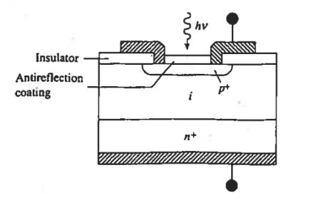
Figure 24: p-i-n photodiode Cross section.
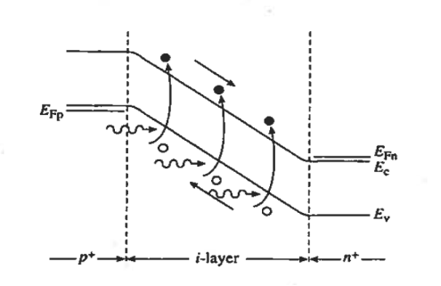
Figure 25: p-i-n photodiode Reverse bias energy band diagram.
It should also be noted than the heavy doping of the outer p and n regions causes the depletion means the minority carriers diffusion lengths in these regions will be relatively small. As a result, the greater part of the photocurrent flowing in a p-i-n photodiode arises from carriers generated in the central depletion region.
Operational advantages of the p-i-n photodiode that have made it one of the most widely employed photodetectors stem, from the existences and tailorability of the i-region.
For one, the diode con be optimized for response at a given wavelength by making the layer width equal to the inverse of the absorption coefficient (1/ ) of the specified wavelength Second, with one of the most photocurrent arising from light absorption to the i-region. Frequency response is greatly enhanced over that of a pn junction photodiode. The large ‘ξ-field is the depleted i-region leads to the rapid collection of photo generated carriers and a maximum frequency response.

Where WI is the width of the I region
Vsat is the saturation drift velocity
If WI = 5 then fmax =20GHz
The WI cannot be made arbitrary small to improve frequency.
The RC time constant associated with the internal series resistance (Rs)and the junction capacitance (CJ = Ks 0A/ WI) increases with decreasing WI and eventually limits the response time of the diode.
The excellent frequency response of the p-i-n photodiode makes it important for use as the photo detector in optical fiber telecommunication.
Q20) What do you mean by p-i-n avalanche?
A20)
Avalanche Photodiode
Avalanche Photodiode are specially constructed p-i-n, pn, or even metal-semiconductor photodiodes that are operated near the avalanche breakdown point. A standard Si avalanche photodiode configuration is shown in figure.
One obvious special structural feature is the guard ring around the junction periphery. As noted in junction curvature leads to early breakdown about the junction periphery. The guard ring minimization of defect creation during device processing are also required to achieve uniform breakdown across the face of the junction. The primary advantage of the avalanche photodiode is a photo-signal gain leading to improvement in the signal-to-noise (S/N) ratio.
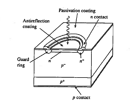
Figure 26: Avalanche Photodiode
As a general rule, amplification of signals is accompanied by amplification of the noise and added noise from the amplifier. Signal pain therefore typically loads to a reduction in the S/N ratio. Inside an avalanche photodiode, however, avalanche multiplication amplifies the photo-signal without amplifying the typically dominant receiver circuit noise. Thus there is an improvement in the S/N ratio until the added avalanche-related noise becomes comparable to the circuit noise.
Avalanche photodiodes made from lnGaAs on lnP and from Ge provide alternatives to the p-i-n photodiode for use in fiber optic telecommunication.
Q21) What value of series resistor is required to limit the current through LED 20mA. Forward voltage drop is 1.6V when 10V Supply is connected.
A21)
Series resistor


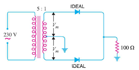
Q22) In a center tap full-wave rectifier is shown in figure. Find (i) The d.c. Output voltage (ii) Peak inverse voltage (iii) Rectification efficiency. Assume the diode is ideal
A22)
Primary to secondary turns = N1 /N2 = 5
R.M.S. Primary Voltage = 230V
R.M.S. Secondary Voltage = R.M.S. Primary Voltage  1/5 =
1/5 =  V
V
Max. Voltage across secondary =46 
 =
=  V
V
Max. Voltage across half secondary windings = Vm = 65/2 =  V
V
(i) Average Current Output

d.c. Output Voltage

(ii) Peak inverse voltage = 65V
(iii) Rectification efficiency =
Since rf =0
Thus Rectification efficiency = 81.2
Q23) In a half-wave rectifier applied input a.c. Power is 100 Watts. The d.c. Output power obtained is 40 watts. (i) What is the rectification efficiency? (ii) What happens to remaining 60 watts?
A23)
(i) Rectification efficiency = (d.c. Output power / a.c. Input power) 100 = 40%
(ii) 40% efficiency of rectification does not mean that 60% of power is lost in the rectifier circuit. In fact, a crystal diode consumes little power due to its small internal resistance.
The 100 Watts a.c. Power consist of 50 Watts positive cycle and 50 Watts negative cycle. However, negative cycle is not of any use in half wave rectifier. Thus
Power Efficiency =(40/50)  100 = 80%
Rectification efficiency is 40% and Power Efficiency is 80%.
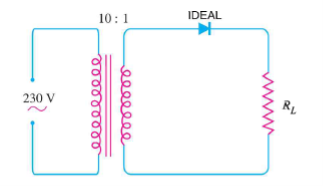
Q24) In a half-wave rectifier applied input a.c. Voltage supplied is 230 V transformer ratio is 10:1. Find (i) The d.c. Output voltage (ii) Peak inverse voltage. Assume the diode is ideal
A24)
Primary to secondary turns = N1 /N2 = 10
R.M.S. Primary Voltage = 230V
Max. Primary Voltage Vpm = 
 R.M.S. Primary Voltage =
 230 = 325.3 V
Max. Secondary Voltage =

(i) 

(ii) During negative half cycle of a.c. Supply. Diode does not conduct. Max. Secondary Voltage across diode =
Peak inverse voltage = 32.53 V
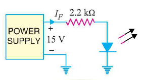
Q25) What value current through LED in following figure. Forward voltage drop is 2V.
A25)
Current through LED, 
Here 
