Unit - 4
Operational Amplifiers
Q1) In a summing amplifier, if R = 1kΩ, Va = +3V, Vb = +8V, Vc = +9V, Vd = +5V and supply voltage is ±15V. Find the output voltage Vo.
A1)
Vo = Sum of all input voltages applied at both the terminals
Vo = Va + Vb + Vc +Vd
Vo = -3 -8 +9 +5
Vo = +3V
Q2) Find the output voltage for the given circuit diagram if Rf = 5kΩ.
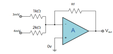
A2)
We know,
Gain (Av) = =
= 
Hence,
Av1 = 
Av2 = 
Now, Output voltage Vo = Sum of the two amplified input signals
Vo = Av1 x V1 + Av2 x V2
Vo =(-5 x 3) + ( -2.5x 4) mV
Vo = -25mV
As the above output voltage is negative hence it is an inverting amplifier.
Q3) OP-Amp is shown in figure. Calculate Rf? Closed loop voltage gain is -100V.
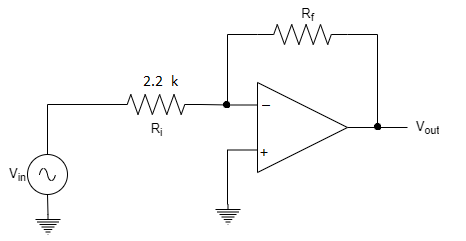
A3)


Q4) Non inverting OP-Amp is shown in figure. Input Voltage 120μV. Find Output Voltage.
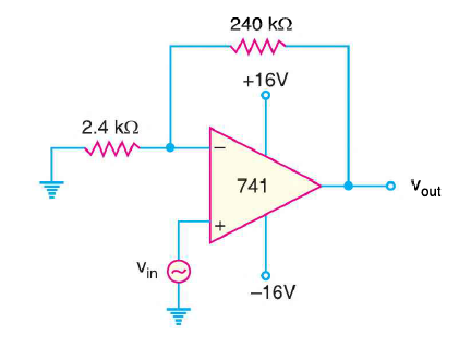
A4)
Voltage gain 
Output voltage 
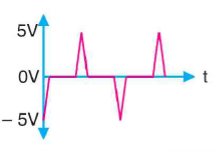
Q5) Figure shows the square wave input to a differentiator circuit. Find the output voltage if input goes from 0V to 5V is 0.1ms.
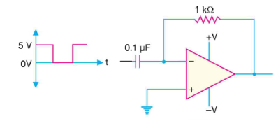
A5)
Output Voltage

=

Output is shown in figure below
Q6) The integrator circuit as shown in the figure has R = 500K Ω and C=1µF. Find and plot the output voltage for the inputs as shown in the figure.
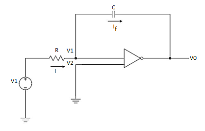

a) b)
c)vi= 2 sin 4tV d) vi= 4tV
A6)
We know that
v0 = - 1/RC  + v0(0)
Here R= 500K Ω and C = 1µF
1/RC = 1/ 500 x 1000 x 1 x 10-6
= 1/RC = 2
= -2  ; vi =- 5V
= -2 
= 10t V
Which means it is a ramp voltage with positive slope.
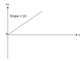
When vi=5V
-2  ; vi = 5V
= -2 
= -10t V
Which means it is a ramp voltage with negative slope.
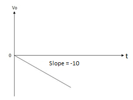
When vi= 2 sin4t V
Vo = -2 
= -4 [-cos 4t] /4 = cos 4t
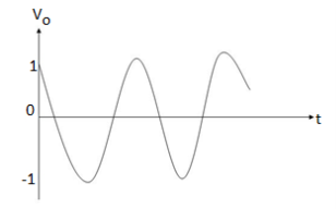
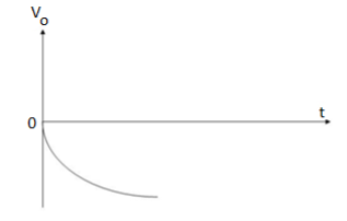
When vi=4t V
Vo = 
= -8 [t2/2] = - 4V
Q7) In the RC network of a Wein bridge oscillator R1 = R2 = 200kΩ, determine the value of each of the capacitor to obtain a frequency of 5kHz.
A7)
F = 
F = 5kHz, = 5000Hz
R1= R2= 200kΩ = 200×103Ω
5000 = 
C =  = 159.15 pF
Q8) Explain Wien -Bridge Oscillator?
A8)
Wien -Bridge Oscillator
In this, phase shift is produced by using 2 transistors. Each produces a phase shift of 180° and hence phase shift of 360° is obtained
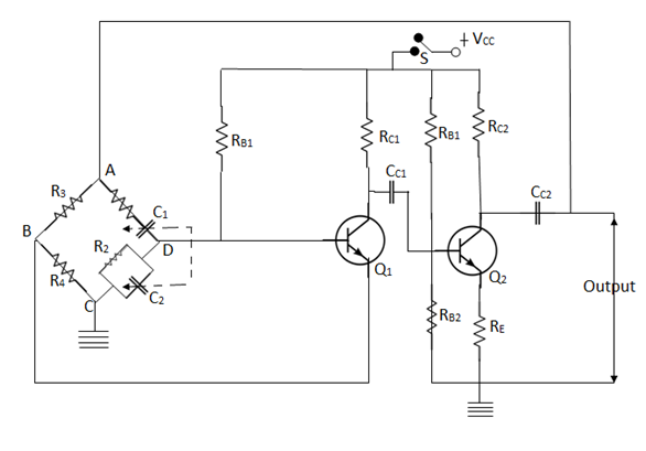
Figure 25: Wein Bridge Oscillator
It is a 2-stage amplifier with R-C bridge circuit. The bridge circuit has 4 arms each containing components R1C1 in Series, R2 C2 in parallel, R3 and R4. Q1 acts as an oscillator and amplifier whereas Q2 Serves as an inverter
When circuit is closed through switch S, the bridge circuit produces the oscillations of frequency whose expression is given by-
F= 
If R1=R2=R and C1= C2 = C then
F = 
A total phase shift of 360° is obtained at the output of the second transistor. A fraction of this output energy is fed back to the oscillatory circuit (bridge) at the upper terminal. This positive feedback is to meet with the losses in the oscillator and hence undamped oscillations are produced.
Advantages-
- It has better stability
- Output is constant
- Overall gain is high
- Frequency can be adjusted by varying C1 and C2
Disadvantages-
- Costly
- Cannot generate frequency>1MHz.
Q9) Derive an Expression for feedback factor (β) and frequency (f) for Wien -Bridge Oscillator?
A9)
Expression for feedback factor (β) and frequency (f)
In order to obtain expression for β and f, we will consider only frequency sensitive arms AD and CD as shown in figure below
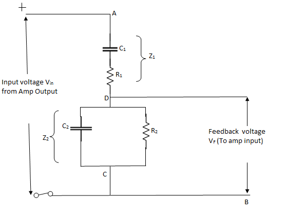
Figure 26: Wein bridge oscillator
Vin is actually the output voltage V0which comes from the amplifier output and voltage across R2C2acts as a feedback voltage VF
Feedback factor β = 
Let impedance of arm AD be Z1 and that of DC be Z2
Therefore VF =  ×Vin{ using voltage divider}
β =  =
=  ………….(1)
Z1= R1 +  =
=  …………..(2)
Z2 = R2 || Xc2=  =
=  ………….(3)
Substituting equation (2) and (3) in (1)
β = 
Substituting jw = S
β = 
β = 
β = 
β = 
Resubstitute jw = S, S2 = j2 w2 = -w2
β = 
β = 
Rationalize the above equation
β =  ……………(4)
The phase shift introduced by the wien bridge circuit at the desired output frequency should be 0°. For that the imaginary part of equation (4) should have a zero value.
WC1R2(1-w2R1R2C1C2) = 0
w2R1R2C1C2 = 1
 =
= 
W = 
F = 
The above equation is the expression for the oscillator frequency.
If we substitute R1 = R2 = R and C1 = C2 = C
F =  or w =
For β, if R1 = R2 = R, C1= C2 = C
β = 
Substituting
W = 
β =  =
=  =
= 
Thus, at the oscillator frequency F, the value of feedback factor β is 
Q10) Discuss zero crossing detector?
A10)
Zero Crossing Detector
An op-amp detector that has the ability to detect the change from positive to negative or negative to a positive level of a sinusoidal waveform is known as a zero- crossing detector.
It is also known to be a square wave generator as the applied input signal is converted into a square wave by the zero -crossing detector.
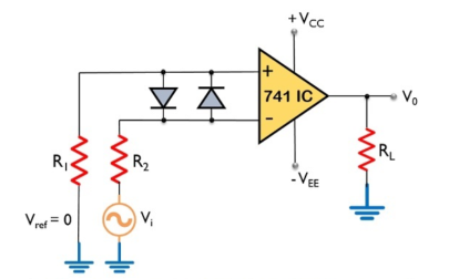
Figure 23: Zero crossing Detector
Here, the input signal Vi is provided to the inverting terminal of the op-amp while the non-inverting terminal is grounded by making use of two resistors R1 and R2.
It detects the point where the input signal crosses zero of the reference voltage level. For every crossing, the saturation level of the output signal changes from one to another.
The reference level is set at 0 and applied at the non-inverting terminal of the op-amp. The sine wave applied at the inverting terminal of the op-amp is compared with the reference level each time the phase of the wave changes either from positive to negative or negative to positive.
Firstly, when positive half of the sinusoidal signal appears at the input. Then the op-amp comparator compares the reference voltage level with the peak level of the applied signal.
Vo = Vref – Vi ---------------------------------------(1)
And we know the reference level is 0, thus
Vo = 0 – ( + Vsat) ----------------------------------------(2)
Therefore, Vo = - Vsat ---------------------------------(3)
During the negative half of the signal, thus the peak will have a negative polarity.
Again
Vo = Vref – Vi ---------------------------------------------(4)
Thus,
Vo = 0 - ( - Vsat) --------------------------------------------------(5)
So, we get
Vo = + Vsat ---------------------------------------------(6)
In this way, the zero -crossing detector detects the change in the level of the applied signal.
Zero crossing detector is also known to be a square wave generator. As the output of the window comparator is nothing but a square wave.
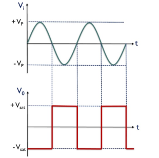
Figure 24: Input and output of zero crossing detector
V0 for the positive half of the applied signal is – Vsat,
This is the reason why we have achieved negative half of the square wave at the output when positive half of the sinusoidal signal is applied. While V0 for the negative half of the sinusoidal signal is + Vsat,
Applications:
- Phase Locked Loop
- Frequency counters and phase meters
Q11) Discuss Log Amplifier?
A11)
Log Amplifier
As the name says it is an amplifier which produces the output proportional to logarithmic of the applied input. The log amplifier using op-amp is shown below. The input is applied through the inverting end of op-amp. As the non-inverting end has voltage zero then by virtual ground concept the voltage at inverting terminal also becomes zero.
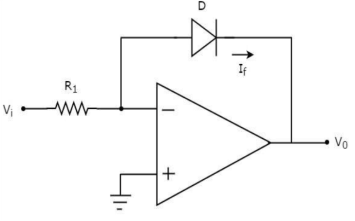
Figure 21: Log Amplifier
The equation for input voltage will be
 +If = 0
If = 
The current flowing through diode is given as

Where:
Is = Saturation Current
Vf = Voltage drop across diode in forward bias
VT = Thermal equivalent voltage
For feedback loop the KVL equation will be
0-Vf -V0 = 0
Vf = -V0
Substituting Vf in above equation of If

Equating both equations of If


Taking natural log of both sides we get


The above equations shows that the output is natural log of the applied input.
Q12) Discuss Anti Log Amplifier?
A12)
Antilog Amplifier
This device produces the output proportional to antilog of input. The inverting op-amp is used in this case as well. The figure below shows an antilog amplifier with its inverting terminal connected to the input end with diode and the non-inverting terminal is grounded.
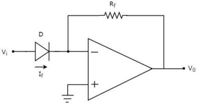
Figure 22: Antilog Amplifier
Applying KCL at input terminal we get


The current flowing through diode is given as

Substituting If in above voltage equation we get


At inverting terminal applying KVL we get


Substituting Vf in equation of V0 we get

The above equations shows that the output is natural antilog of the applied input.
Q13) Discuss Integrator?
A13)
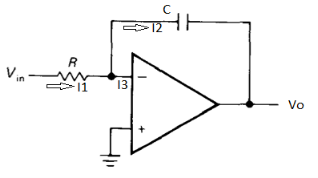
Figure 20: Integrator
- It is a circuit which provides output voltage Vo as an integral form of input voltage Vin.
- It is obtained by using an inverting amplifier and replacing its feedback resistor Rf with a capacitor C.
- Hence,

Ignoring I3 we have, I3 ≈ 0
So, I1 ≈ I2.
- We know current across the capacitor is given by,

- Now by applying Kirchoffs current law,

However, V = 0 because gain A is very large

Integrating both sides we get


 + Q
+ Q
Where Q is the integration constant and is proportional to Vo at t = 0 sec.
Therefore, voltage Vo is directly proportional to Vin and inversely proportional to constant RC.
Frequency response of basic integrator circuit is given by,
 ( for 0 db gain)
Q14) Discuss differentiator Op-amp?
A14)
- A differentiator is a circuit that performs differentiation operation. Hence, the output is a derivative of input.
- In an inverting amplifier, if input resistor is replaced by a capacitor then a differentiator circuit is formed.
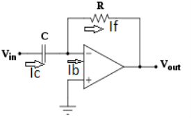
Figure 18: Differentiator
- In the above fig. On applying Kirchhoff’s law we get,

Since Ib = 0 then,
Ic ≈ If

Since Gain A is very large hence, V1 = 0

Or 
- So, the output voltage is RC times the negative rate of change of input voltage.
- When input is a cosine wave, output is a sine wave i.e it performs the inverse function of integrator circuit.
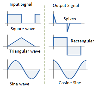
Figure 19: Input and output waveform of differentiator
Frequency response of basic differentiator circuit is given by,
 ( for 0 db gain)
Q15) Discuss subtractor Op-amp?
A15)
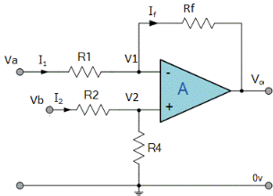
Figure 17: Difference amplifier
- Here input can be provided simultaneously at both the terminals of amplifier.
- Voltage signal Va is applied at one input terminal and another voltage signal Vb onto the other input terminal then resultant output voltage is proportional to the “Difference” between the input voltages Va and Vb.
- Vo = Vb - Va
- Now by applying superposition theorem we get,


Summing point, V1 = V2 and
V2 = Vb
If Vb = 0 then 
And Va = 0 then 
Vo = -V01 + V02
Vo =  +
+ 
If R1 = R2 and Rf = R4 then

And if R1 = R2 = Rf = R4 =R then
Vo = Vb – Va
Hence, is known as a Unity Gain Differential Amplifier.
Q16) Discuss Non-Inverting Op-amp?
A16)
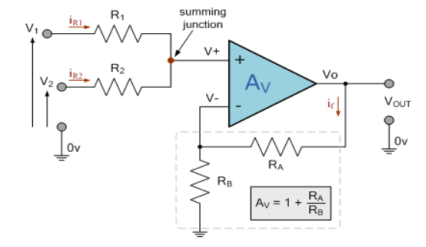
Figure 16: Non-Inverting Summing Amplifier
Applying KCL to the above circuit we have
IR1+IR2 = 0
 =
=  = 0
= 0
When R1 = R2 =R
V+ = 
The voltage gain for non-inverting summing amplifier is given as
AV = Vout/Vin =  = 1+
= 1+
Vout= [1+ ]
] 
Q17) Discuss Inverting Op-amp?
A17)
Inverting Amplifier
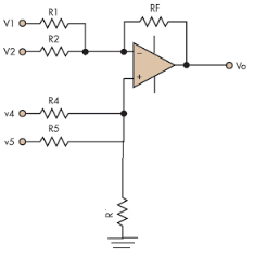
Figure 15: Summing amplifier
- In the above figure, each terminal is connected with two input sources through resistors. V1 and V2 is connected to the inverting terminal and V4 and V5 is connected to the non-inverting terminal.
- Assuming R1=R2=R4=R5=RF=R.
- Now, on applying superposition theorem, for finding output voltage due to V1 alone, keep V2=V4=V5=0V.
- Hence, now the circuit acts as an inverting amplifier.
- Therefore,

- Similarly,

- Now, for V4, voltages V1=V2=V5=0V then the circuit behaves as a non-inverting amplifier.


Hence,


Similarly,

So, the resultant output voltage by all the 4 input voltages is given by,
Vo = V01 + V02 + V04 +V05
Vo = -V1 – V2 +V4 + V5
The output voltage Vo is equivalent to the sum all input voltages applied at both the terminals.
Q18) Discuss the concept of concept of virtual ground?
A18)
Concept of Virtual Ground
Virtual Ground simply indicates that this concept is virtual. This is different from real ground but considered as equivalent to ground.
Let us suppose, In Op-amps the term virtual ground refers to that the voltage at that particular node is almost equal to ground voltage (0V). It is not connected to ground physically.
This concept is an important and useful for Op-amp analysis and make calculations very simple.
Virtual ground in inverting Op-amp. We know that an ideal Op-amp will provide infinite voltage gain.
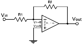
Figure 13: Virtual ground
The gain will be very high for real Op-amps. For calculation purposes it is considered as infinite.
Gain = Vo/Vin
As gain is infinite, Vin = 0
Vin = V2 – V1
Here V1 = 0
As in the above circuit V1 is grounded. Thus V2 also will be at ground potential.
V2 = 0
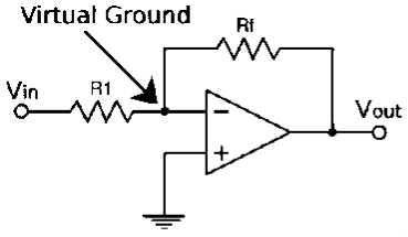
Figure 14: Virtual ground
Q19) How Virtual ground is different from real ground?
A19)
Virtual Ground | Real Ground |
Virtual Ground is a concept that concept is an important and useful for Op-amp analysis and make calculations very simple. | Real Ground is a terminal which is physically connected to ground or earth. This point acts as the reference point for the entire circuit. |
Voltage is approximately Zero | Voltage is Zero |
Not able to sink infinite current | It is an infinite current sink |
Not electrically connected to Ground | Electrically connected to Ground |
Q20) Explain the term Slew rate and CMRR?
A20)
Slew Rate
The slew rate is a parameter that describes the operating speed of an op-amp. It represents the rate that can change per unit time stipulated by the output voltage.
For example, 1V/us indicates that the voltage can change by 1V in 1us. Ideal op-amps make it possible to faithfully output an output signal for any input signal. However, in reality slew rate limits do exist.
When supplying a rectangular pulse at the input with a steep rise and fall, this indicates the possible degree of change in the output voltage per unit time.

Figure 9: Voltage Follower
The rise and fall slew rates are calculated by the following equations:
SRr = ∆ V / ∆ Tr
SRf = ∆ V / ∆ Tf
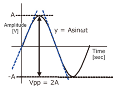
Figure 10: Slew Rate Calculation
Calculate the slew rate
The output is given by
y=Asinωt
The slew rate is the slope of the tangent of the sine wave, differentiating the above equation.
Dy / Dt = Aω cosωt ωt=0
The slew rate is
SR=Aω ω=2πf
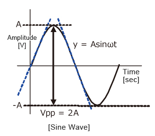
Figure 11: Sine wave amplitude
Since the amplitude of the sine wave becomes Vpp=2A (peak-to-peak), the equation can be modified as follows.


This frequency(f) is referred to as the full power bandwidth. These are conditions where the amplification factor in the op-amp has not been set, in other words the relationship of the frequency and amplitude (within the output voltage range) that can be output by the op-amp in a voltage follower circuit.
CMRR
It is the ratio of differential voltage gain Ad to the common mode voltage gain Acm.
CMRR = 
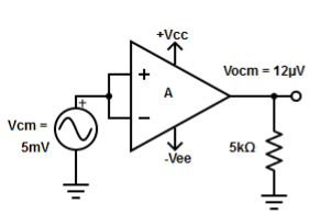
Figure 12: Common Mode Configuration
The common mode voltage gain from above figure can be
 =
= 
Where:
Vocm = output common mode voltage
Vcm = input common mode voltage
Acm = common mode voltage gain
In normal cases the value of Ad is large and Acm is very small making the value of CMRR very high.
Q21) Discuss frequency response for Op-amp?
A21)
A characteristic open-loop frequency response plot is shown in figure.
At very low frequencies, the op-amp applies the maximum open-loop gain to differentiate it from the gain at higher frequencies. Gain decreases as the frequency increases, gain decreases.
There is a transition from stable gain to decreasing gain at the corner frequency. Finally the slope stabilizes. The gain decreases by 20 dB for every factor of 10 increases in input frequency.
The gain begins to decrease at such a low frequency.
This type of frequency response makes the op-amp when used in a negative-feedback configuration less likely to oscillate when used in a negative-feedback configuration.
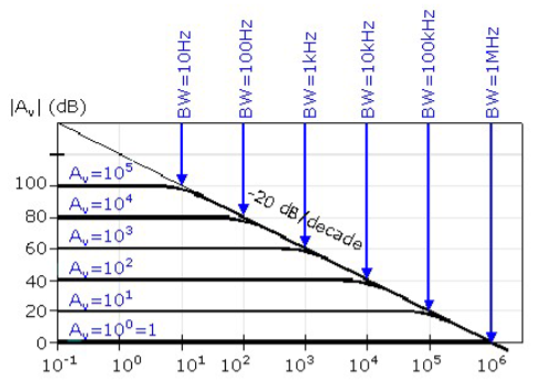
Figure 8: Frequency Response
In the above figure, take an example of voltage gain.
The vertical axis expressed in decibels (dB) and the corresponding closed loop gain noted in blue. The horizontal axis in this figure is frequency in Hertz using a logarithmic scale.
For this first order system, the bandwidth is the upper break frequency. It is also called the corner frequency. It is defined as the point at which we make the -3 dB correction from the straight line approximation.
An important characteristic of this figure is that the gain- bandwidth product (GBP) is constant. Logarithmic plot never goes to zero and the GBP must remain constant. The lowest frequency where this is true is considered the zero frequency point.
Q22) Discuss the Block Diagram of Operational Amplifier?
A22)
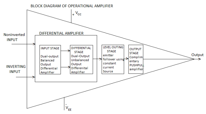
Figure 1: Block Diagram of Operational Amplifier (Op-Amp)
- The op-amp begins with a differential amplifier stage, which operates in the differential mode. Thus the inputs noted with ‘+’ & ‘- ‘ .
- The positive sign is for the non-inverting input and negative is for the inverting input.
- The non-inverting input is the ac signal (or dc) applied to the differential amplifier which produces the same polarity of the signal at the output of op-amp.
- The inverting signal input is the ac signal (or dc) applied to the differential amplifier. This produces 180 degrees out of phase signal at the output.
- The inverting and non-inverting inputs are provided to the input stage which is a dual input, balanced output differential amplifier.
- The voltage gain required for the amplifier is provided in this stage along with the input resistance for the op-amp.
- The output of the initial stage is given to the intermediate stage, which is driven by the output of the input stage.
- In this stage direct coupling is used, which makes the dc voltage at the output of the intermediate stage above ground potential. Therefore, the dc level at its output must be shifted down to 0Volts with respect to the ground.
- For this, the level shifting stage is used where usually an emitter follower with the constant current source is applied.
- The level shifted signal is then given to the output stage where a push-pull amplifier increases the output voltage swing of the signal and also increases the current supplying capability of the op-amp.
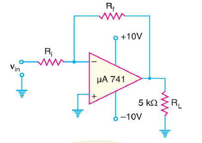
Q23) Determine operating frequency for given circuit. Slew rate is 0.5V/μs.
A23)
Operating frequency for given circuit


Q24) Differential gain of a Differential amplifier is 2000V. Common mode gain is 0.2. Calculate CMRR in dB?
A 24)


Q25) Differential amplifier has differential output 1V and input 10V and output 5V with Common mode input 10mV. Calculate CMRR in dB?
A25)
Differential gain, 
Common-mode gain, 
