Unit - 4
Introduction to Computer Organization
Q1) Write a Short note on Input-Output Interface. Explain its Function.
A1)
The Input-Output Interface (I/O) is a means for moving data between internal storage devices, such as memory, and external peripheral devices. A peripheral device, often known as an input-output device, is a device that provides input and output for a computer. Consider the following scenario: Input devices, such as a keyboard and mouse, offer input to the computer, and output devices, such as a monitor and printer, offer output to the computer. In addition to external hard drives, several peripheral devices that can provide both input and output are also available.
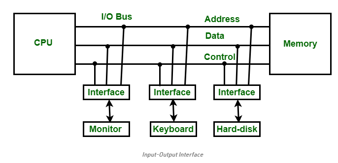
The sole purpose of peripheral devices in a microcomputer-based system is to offer unique communication lines for connecting them with the CPU. Communication links are required to resolve disparities between peripheral devices and the CPU.
The following are the main differences:
1. Peripheral devices are electromagnetic and electromechanical in nature. The CPU is electrical in nature. The modes of functioning of peripheral devices and the CPU differ significantly.
2. Because peripheral devices communicate data at a slower rate than the CPU, there is also a synchronisation mechanism.
3. Data code and formats in peripheral devices differ from those in the CPU and memory
4. Peripheral device operating modes differ, and each can be managed to avoid interfering with the operation of other peripheral devices attached to the CPU.
Additional hardware is required to resolve disparities between the CPU and peripheral devices, as well as to supervise and synchronise all input and output devices.
Functions of Input-Output Interface:
1. It's utilised to keep the CPU's operating speed in sync with the input-output devices.
2. It chooses an input-output device that is appropriate for the input-output device's interpretation.
3. It can send out signals such as control and timing signals.
4. Data buffering is possible through the data bus in this case.
5. There are several types of error detectors.
6. It converts serial data to parallel data and the other way around.
7. It can also convert digital data to analogue signals and the other way around.
Q2) What is the difference between an input and output device?
A2)
An input device transmits data to a computer system, which is then processed, and an output device reproduces or displays the results. Input devices only allow data to be entered into a computer, whereas output devices only receive data from another device.
Because they can either accept data input from a human or emit data created by a computer, most devices are either input or output devices. However, some devices, known as I/O devices (input/output devices), can accept input and show output.
A keyboard, for example, sends electrical signals that are received as input, as illustrated in the top half of the image. The computer then interprets the signals and displays them on the monitor as text or graphics. The computer delivers or outputs data to a printer in the lower half of the image. The data is then printed on a piece of paper, which is also referred to as output.
Input/output (I/O) devices
An input/output device can take data from people or another device (input) and transfer it to another device (output) (output). The following are some examples of input/output devices.
1. CD-RW and DVD-RW drives - These drives receive data from a computer (input) and copy it on a readable CD or DVD. The drive may also send data from a CD or DVD (output) to a computer.
2. USB flash drive - A USB flash drive receives and saves data from a computer (input). The drive can also deliver data to a computer or other device (output).
Q3) Define Computer Memory and Explain its Types.
A3)
Computer memory refers to the various forms of data storage technology that a computer can employ, such as RAM, ROM, and flash memory.
Some computer memory is designed to be extremely fast, allowing the central processor unit (CPU) to quickly retrieve data stored there. Other varieties are meant to be extremely low-cost, allowing enormous volumes of data to be stored there without breaking the bank.
Another difference in computer memory is that some types are non-volatile, meaning they can keep data for a long time even after the power is turned off. And then there are volatile varieties, which are generally speedier but lose all of the data they contain as soon as the power is turned off.
A computer system is made up of a mix of various types of computer memory, and the exact arrangement can be tweaked to achieve the best data processing speed, lowest cost, or a compromise between the two.
Types of Computer Memory: Primary and Secondary
Although there are many different types of memory in a computer, the most basic distinction is between primary memory, also known as system memory, and secondary memory, often known as storage.
The main distinction between primary and secondary memory is access speed.
Primary memory
Includes ROM and RAM, and is located close to the CPU on the computer motherboard, enabling the CPU to read data from primary memory very quickly indeed. It is used to store data that the CPU needs imminently so that it does not have to wait for it to be delivered.
Secondary memory
Data, on the other hand, normally housed in a separate storage device, such as a hard disc drive or solid state drive (SSD), that is connected to the computer system either directly or over a network. Secondary memory has a lower cost per gigabyte, but read and write speeds are much slower.
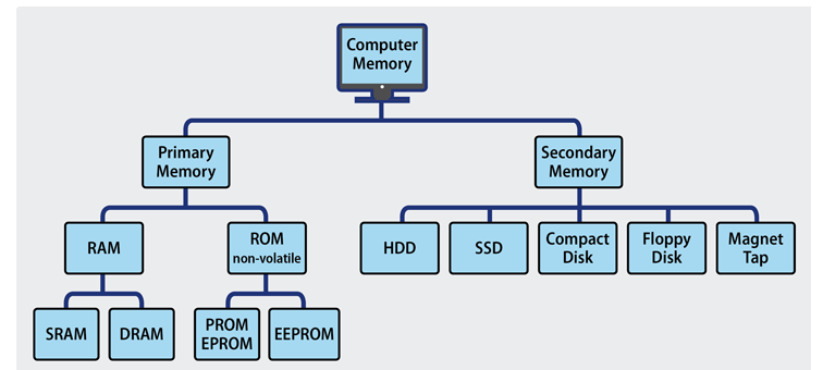
A diverse range of computer memory types has been used during the course of computer evolution, each with its own set of strengths and disadvantages.
Q4) Compare Byte Addressing vs. Word Addressing.
A4)
N address lines can be used to specify 2N separate addresses, numbered 0 through 2N – 1. As previously stated, N address lines can be used to define 2N separate addresses, numbered 0 through 2N – 1. We've moved on to enquiring about the size of the addressable items. Most current computers are byte-addressable, which means that the addressable item is 8 bits or one byte in size. Other options are available. We'll now look at the benefits and drawbacks of being able to address larger entities.
Consider a computer with a 16–bit address space as an example. There would be 65,536 (64K = 216) addressable entities on the system. The maximum memory size is determined by the addressable entity's size.
64 KB of byte addressable memory
128 KB, 16-bit Word Addressable
256 KB, 32-bit Word Addressable
The maximum memory size for a given address space is greater for larger addressable entities. This may be advantageous for some applications, but it is mitigated by the extremely huge address spaces we already have: 32 bits now, 64 bits soon.
When we consider programmes that process data one byte at a time, the benefits of byte-addressability become evident. In a byte-addressable system, accessing a single byte needs simply issuing a single address. In a 16-bit word-addressable system, computing the address of the word containing the byte, fetching that word, and finally extracting the byte from the two-byte word are all required steps. Although byte extraction procedures are well understood, they are less efficient than retrieving the byte directly. As a result, many current machines can be addressed in bytes.
Q5) Explain Memory as a Collection of Chips.
A5)
A group of memory chips makes up all modern computer memory. Interleaving is the technique of translating an address space into a number of smaller chips.
Consider a computer with 256 MB of byte-addressable memory, a 32–bit address space, and byte-addressable memory.
There is 228 bytes of RAM available. This computer is based on the author's personal computer, however the memory size has been changed to a power of two to simplify the example. The MAR addresses can be thought of as 32–bit unsigned integers with high order bit A31 and low order bit A0. We state that only 28-bit addresses are valid, ignoring issues of virtual addressing (essential for operating systems), and that a valid address has the following form.

All current computers have multiple chips in their memory that are combined to cover the range of permissible addresses. Assume that the fundamental memory chips in our case are 4MB chips. The 256 MB memory would be made up of 64 chips with the following address space:
6 bits to pick the memory chip (26 = 64) and 22 bits to pick the byte (222 = 4•220 = 4M) within the chip.
Which bits choose the chip and which bits are transferred to the chip is the question. High-order memory interleaving and low-order memory interleaving are two popular choices. Only low-order memory interleaving will be discussed, in which the lower-order address bits pick the chip and the higher-order bits pick the byte.

Low-order interleaving provides a number of performance benefits. This is because subsequent bytes are stored in different chips, so byte 0 is in chip 0, byte 1 is in chip 1, and so on. In our case,
Chip 0 contains bytes 0, 64, 128, 192, etc., and
Chip 1 contains bytes 1, 65, 129, 193, etc., and
Chip 63 contains bytes 63, 127, 191, 255, etc.
Assume the computer's memory and CPU are connected by a 128-bit data bus. It would be feasible to read or write sixteen bytes at a time using the low-order interleaved memory described above, resulting in a memory that is close to 16 times faster. It's worth noting that the gain in memory performance for such an arrangement is constrained by two factors.
1) The memory's chip count, which is 64 in this case.
2) The data bus width in bytes — in this case, 16 is the lower value.
A 6–to–64 decoder or a pair of 6–to–64 decoders could be used in a design to achieve such an address system.
Q6) What is Memory Organization in Computer Architecture?
A6)
The term "memory unit" refers to a grouping of storage units or devices. The binary information is stored in bits in the memory unit. Memory/storage is generally divided into two categories:
● Volatile Memory: When the power is turned off, the data is lost.
● Non-Volatile Memory: This is a permanent storage device that does not lose data even if the power is turned off.
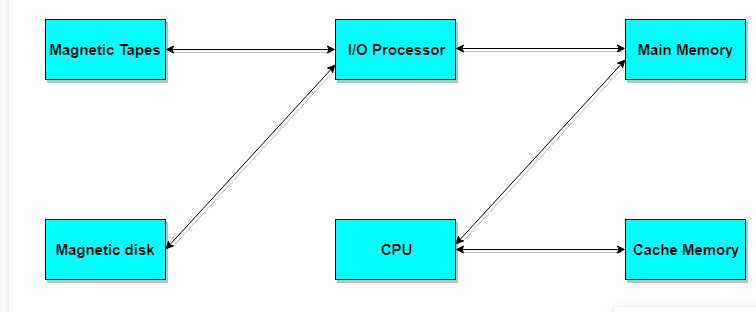
The access time of auxiliary memory is typically 1000 times that of main memory, putting it at the bottom of the hierarchy.
The primary memory is in the middle because it has an input/output processor (I/O) that allows it to interface directly with the CPU and auxiliary memory devices.
When the CPU requires a programme that is not in main memory, it is retrieved from auxiliary memory. Auxiliary memory is used to store programmes that are not currently in use in main memory, freeing up space in main memory for other programmes.
Program data that is currently being executed in the CPU is stored in the cache memory. The access time ratio between cache memory and main memory is roughly 1 to 710 milliseconds.
Q7) Explain Pin diagram of memory chips.
A7)
Except for the WR pin, which is present in RAM but not in a ROM, RAM and ROM have the identical pins. Let's take a look at the pins one by one.
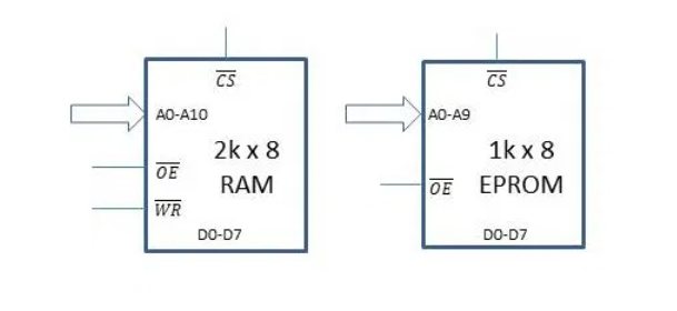
- Data pins: Because each memory location contains eight bits, the memory chip has eight data lines D0-D7 attached to it.
- Address pins: The number of address pins depends on the size of the memory. In this case, a memory of size 1 kB x 8 will have 210 different memory locations. Hence, it will have ten address lines A0 to A9. Similarly, the 2 kB RAM will have 211 different memory locations. So, there are 11 address lines A0-A10.
- CS pin: When this pin is enabled, the memory chip recognises that the CPU is attempting to communicate with it and responds appropriately. This signal must be generated for each chip based on the range of addresses assigned to them. Essentially, we choose a chip only when it is required. This is done through the Chip Select (CS) pin.
- OE pin: The memory chip can output data onto the data bus when this active-low output enable pin is enabled.
- WR pin: When this active-low memory write pin is activated, data from the data bus is written to the memory chip at the address bus's defined location.
- VCC and GND pins: These pins are used to power the integrated circuits. These pins will not be shown in the diagram for clarity.
- In 8085, there are three different types of buses: address buses, data buses, and control buses. The memory chip will be attached to each of these buses.
Q8) Write Short note on Serial in Serial Out (SISO) Shift Register.
A8)
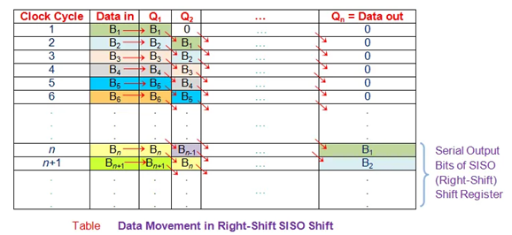
Serial In Serial Out (SISO) shift registers are a type of shift register in which data is loaded and retrieved from the shift register in serial mode. Figure 1 depicts an n-bit synchronous SISO shift register that is responsive to the clock pulse's positive edge. At the input of the first flip-flop, the data word to be stored is fed bit by bit. Furthermore, all other flip-flops' inputs (save the first, FF1) are driven by the outputs of the ones before them, for example, the input of FF2 is controlled by the output of FF1. Finally, the data saved in the register is serially accessed at the output pin of the nth flip-flop.

Initially, all of the register's flip-flops are cleared by applying a high voltage to their clear pins. Following that, the input data word is serially supplied to FF1.
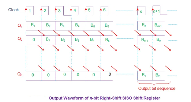
As soon as the first leading edge of the clock emerges, the bit occurring at the D1 pin (B1) is stored into FF1. B1 is saved in FF2 during the second clock tick, while a new bit is entered into FF1 (B2).
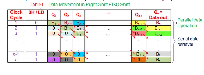
Every rising edge of the clock pulse causes a similar shift in data bits. This means that the data in the register shifts one bit to the right for every single clock pulse. As a result, the design in Figure 1 is known as a right-shift SISO shift register. The first bit of an input word appears at the output of the nth flip-flop for the nth clock tick after the data transfer has been explained. When more clock cycles are applied, the serial output is the next set of bits from the input data word (Table I). Figure 2 depicts the waveforms related to the same.
A left-shift SISO shift-register can exist in the same way as the right-shift SISO shift-register depicted. The operating idea stays the same, with the exception that data will be moved from right to left.

Q9) Explain Shift register counter in Details.
A9)
Shift Register Counters are shift registers that have their outputs wired back to their inputs to produce certain sequences. There are two types of these:
1. Ring Counter –
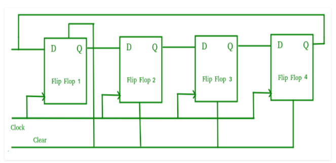
A ring counter is a shift register counter in which the output of the first flip flop is connected to the output of the second flip flop, and so on, with the output of the last flip flop being fed back to the input of the first flip flop. As long as clock pulses are applied, the data pattern within the shift register will circulate.
A Ring Counter is shown in the logic circuit below. The circuit is made up of four D flip-flops that are connected together. The data pattern will repeat every four clock pulses because the circuit consists of four flip flops, as illustrated in the truth table below:
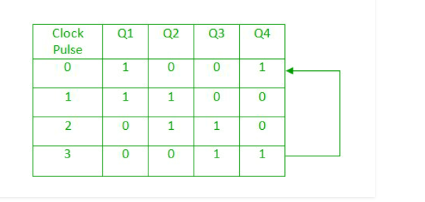
Ring counters are commonly utilised since they are self-decoding. To determine what state the counter is in, no further decoding circuit is required.
2. Johnson Counter –
A Johnson counter is a shift register counter in which the first flip flop's output is connected to the second flip flop's output, and so on, with the inverted output of the last flip flop being fed back to the first flip flop's input. Twisted ring counters are another name for them.
A Johnson Counter is shown in the logic circuit below. The circuit is made up of four D flip-flops that are connected together. A mod-2n counter is an n-stage Johnson counter that produces a count sequence of 2n different states. The data pattern will repeat every eight clock pulses because the circuit consists of four flip flops, as shown in the truth table below:
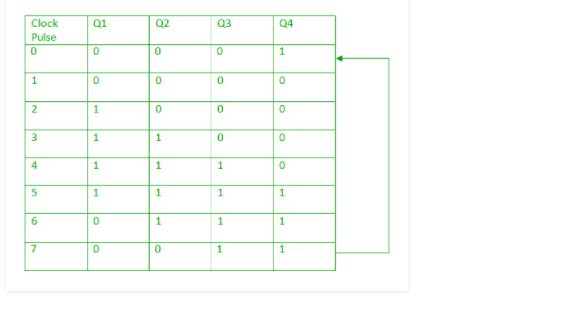
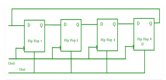
1. The fundamental advantage of the Johnson counter over the ring counter is that it only requires n flip-flops to circulate a given data and generate a sequence of 2n states.
Applications of shift Registers –
1. Shift registers are used to store temporary data.
2. Data transport and manipulation are also done with shift registers.
3. To add time delay to digital circuits, serial-in serial-out and parallel-in parallel-out shift registers are utilised.
4. The serial-in parallel-out shift register is employed in communication lines where demultiplexing of a data line into numerous parallel lines is necessary.
5. To convert parallel data to serial data, a Parallel in Serial out shift register is utilised.
Q10) Write Short Note on Shift Register.
A10)
Another form of sequential logic circuit that can be used to store or transport binary data is the Shift Register.
The data on its inputs is loaded into this sequential device, which subsequently moves or "shifts" it to its output once every clock cycle, hence the name Shift Register.
A shift register is made up of many single-bit "D-Type Data Latches," one for each data bit, either a logic "0" or "1," coupled in a serial type daisy-chain arrangement, with the output of one latch becoming the input of the next, and so on.
Data bits can be fed in or out of a shift register serially, that is, one after the other from the left or right, or in a parallel configuration, all at the same time.
The number of individual data latches required to build up a single Shift Register device is normally dictated by the number of bits to be stored with the most common being 8-bits (one byte) wide formed from eight distinct data latches.
Shift Registers are used in calculators and computers for data storage or data transfer. They are typically used to store data such as two binary numbers before they are added together, or to transform data from serial to parallel or parallel to serial formats. A single shift register's individual data latches are all driven by the same clock ( Clk ) signal, making them synchronous devices.
Shift register ICs typically have a clear or reset connection, allowing them to be "SET" or "RESET" as needed. Shift registers generally function in one of four modes, with the basic data transfer through a shift register being:
Serial-in to Parallel-out (SIPO) - the register is filled one bit at a time with serial data, with the stored data available in parallel form at the output.
Serial-in to Serial-out (SISO) - under clock control, data is serially shifted "IN" and "OUT" of the register, one bit at a time in either a left or right direction
Parallel-in to Serial-out (PISO) - parallel data is concurrently loaded into the register and serially moved out of the register one bit at a time under clock control.
Parallel-in to Parallel-out (PIPO) - the parallel data is loaded into the register at the same time and transferred to their respective outputs at the same time using the same clock pulse.
The following graphic depicts the effect of data movement from left to right through a shift register:
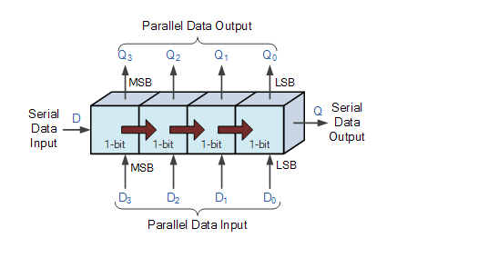
A shift register's directional movement of data can be to the left (left shifting), to the right (right shifting), left-in but right-out (rotation), or both left and right shifting within the same register, resulting in bidirectional data movement. It is assumed in this course that all data shifts to the right (right shifting).
Q11) What is Parallel in Serial Out (PISO) Shift Register?
A11)
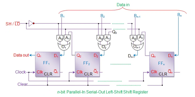
Data is loaded into Parallel In Serial Out (PISO) shift registers in parallel format and retrieved serially. In addition to the fundamental register components (flip-flops) fed with clock and clear pins, Figure depicts a PISO shift register with a control-line and combinational circuit (AND and OR gates).
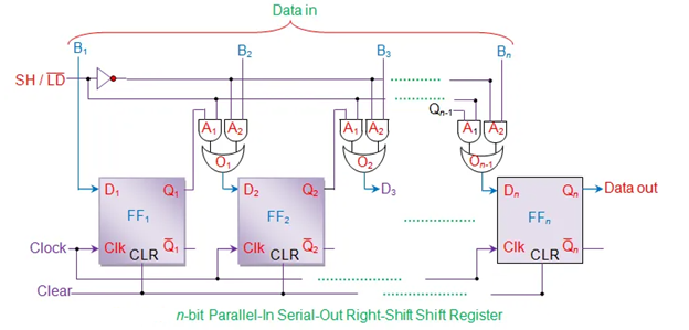
The SH/LD control line is used to select the shift register's functionality between shift and load at any given time. This is because when the SH/LD line is set to low, all combinational circuits' A2 AND gates become active, while the A1 gates become dormant.
As a result, the bits of the input data word (Data in) that appear as inputs to the gates A2 are sent on as OR gate outputs at each combinational circuit. At the appearance of the first leading edge of the clock, the various bits of the Data in are loaded/stored into respective flip-flops (except the bit B1 which gets directly stored into FF1 at the first clock tick). This means that at the same clock tick, all the bits of the input data word are stored in the register components.
The SH/LD line is then driven high, activating the gates A1 of the combinational circuits and deactivating the gates A2. This enables the output bit of each flip-flop (save the last flip-flop FFn) to appear as the output of the OR gate driving the very-next flip-flop, i.e. the output bit of FF1 (Q1) appears as the output of OR gate 1 (O1) connected to D2; Q2 = output of O2 = D3, and so on. If the rising edge of the clock pulse appears at this point, Q1 appears at Q2, Q2 occurs at Q3, and so on. Qn-1 shows up at Qn.
This is nothing more than a one-bit right-shift of the data stored in the register. Similarly, one bit escapes the PISO shift register through the output pin of the nth flip-flop (Data out = Qn of FFn), which is nothing but the serial output, for each of the additional clock pulses applied. As a result, obtaining the whole n-bit input data word as a serial output of the PISO shift register needs n clock cycles.
Table depicts the PISO shift register's truth table, which emphasises the loading and retrieval processes, whereas Figure 2 depicts the associated wave patterns.
The data bits within the register can be shifted from right to left by minimally altering the design of Figure, resulting in a left-shift PISO shift-register. The core functioning idea, however, has not changed.
Q12) Write Short note on Shift Registers in Digital Logic.
A12)
A single bit of binary data can be stored in a flip flop (1or 0). However, numerous flip flops are required to store several bits of data. To hold n bits of data, N flip flops must be connected in a specific order. A register is a device that is used to store this type of data. It consists of a series of flip flops used to hold numerous bits of data.
With the use of shift registers, the information held in these registers can be transferred. A shift register is a collection of flip flops that can hold multiple bits of information. By applying clock pulses to the bits contained in such registers, they can be made to move within the registers and in and out of the registers. By connecting n flip-flops, each of which holds a single bit of data, an n-bit shift register can be created.
"Shift left registers" are the registers that shift the bits to the left.
"Shift right registers" are the registers that shift the bits to the right.
Shift registers are basically of 4 types. These are:
1. Shift register with serial in and serial out.
2. Shift register with serial in parallel out.
3. Shift register (Parallel In Serial Out)
4. Shift register with parallel in parallel out.
Serial-In Serial-Out Shift Register (SISO) –
Serial-In Serial-Out shift register is a shift register that accepts serial input (one bit at a time through a single data line) and outputs serial data. The data leaves the shift register one bit at a time in a serial pattern because there is only one output, hence the term Serial-In Serial-Out Shift Register.
A serial-in serial-out shift register is shown in the logic circuit below. The circuit is made up of four D flip-flops connected in a serial fashion. Because each flip flop receives the same clock signal, they are all synchronised with one another.
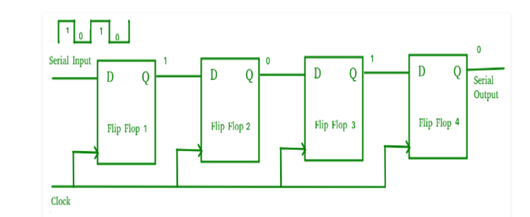
The above circuit is an example of a shift right register, which accepts serial data from the flip flop's left side. A SISO's principal function is to act as a delay element.
Serial-In Parallel-Out shift Register (SIPO) –
Serial-In Parallel-Out shift registers allow serial input (one bit at a time through a single data line) and provide parallel output.
A serial-in-parallel-out shift register is shown in the logic circuit below. The circuit is made up of four D flip-flops that are connected together. To RESET the flip flops, the clear (CLR) signal is connected to them in addition to the clock signal. The first flip flop's output is connected to the next flip flop's input, and so on. Because each flip flop receives the same clock signal, they are all synchronised with one another.
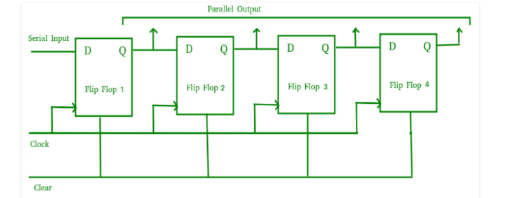
The above circuit is an example of a shift right register, which takes serial data from the flip flop's left side and produces a parallel output. Because the principal application of the SIPO register is to transform serial data into parallel data, they are utilised in communication lines when demultiplexing of a data line into several parallel lines is necessary.
Q13) Write short note on Universal Shift Register. Explain its Construction.
A13)
The universal shift register is defined as "a register that may be used to shift data in both directions, such as left and right, as well as load parallel data."
The three types of operations that this register can do are listed below.
1. Loading in parallel
2. Making a left turn
3. Shifting to the right.
This means the universal shift register can both store and send data in simultaneously. Similarly, by using shift left and shift right operations, data can be stored and transferred in a serial route.
Simply put, the universal shift register will input data in either serial or parallel and produce output in either serial or parallel, depending on our needs. It's known as the Universal Shift Register because it can perform left and right shifts, serial to serial, serial to parallel, parallel to serial, and parallel to parallel operations.
Construction
Take a look at the universal shift register logic gate representation below. The mode input is connected directly to the MUX input, while the reversed mode input (through the NOT gate) is routed to the upper stage flip flops' inputs.
The inputs D1, D2, D3, and D4 are connected in parallel, as are the outputs Q1, Q2, Q3, and Q4. For both left and right shift, it features a serial input pin that feeds data into the register. Below is a logic diagram for a four-bit universal shift register.
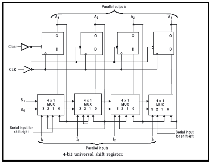
The circuit diagram of a 4 bit bidirectional universal shift register is shown below.
Q14) Write the Applications of Universal Shift Registers.
A14)
Registers are employed in digital electrical devices such as computers for a variety of purposes.
1. Temporary data storage
2. Data transfer
3. Data manipulation
4. As counters.
Computers employ shift registers as memory elements. All digital systems must store huge amounts of data efficiently; to do so, we employ storage elements such as RAM and other types of registers.
Registers are used to perform several operations in digital systems, such as division and multiplication. Data is conveyed using serial shift registers and other similar devices.
Digital clocks, frequency counters, and binary counters are examples of counters.
For time delays, serial in – serial out registers are utilised.
The data is converted from serial to parallel form using serial in – parallel out registers. As a result, these are also known as "Serial to Parallel Converters."
The data is converted from parallel to serial form using parallel in – serial out registers. As a result, they're also known as "parallel to serial converters."
Delay Line
The most common application of shift registers is the delay line. To add time delay to digital circuitry, a serial in serial out shift register is utilised. The following formula can be used to compute the time delay.
Δt = N * 1 / fc
N stands for the number of stages / flip flops, while fC stands for the clock frequency.
As a result, at output, an input pulse is delayed by t. The clock signal frequency or flip flops in the shift register regulate the amount of time delay.
Q15) What is Ring Counter in Digital Logic? Explain Its Working Also.
A15)
Shift resisters are commonly used in ring counters. The ring counter is nearly identical to the shift counter. The main difference is that in a ring counter, the output of the last flip-flop is connected to the input of the first flip-flop, whereas in a shift resister, it is taken as output. Except for that, everything else is the same.
The number of states in the Ring counter equals the number of flip-flops utilised.
So we'll need four flip-flops to make a 4-bit Ring counter.
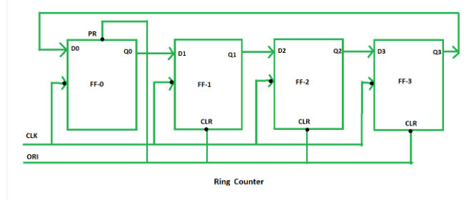
The clock pulse (CLK) is applied to all of the flip-flops at the same time in this diagram. As a result, it's a synchronised counter.
We also use Overriding input (ORI) for each flip-flop here. The ORIs are Preset (PR) and Clear (CLR).
When PR is 0 and the output is 1, the result is 1. When CLR is 0, the output is also 0. PR and CLR are both active low signals that always operate at a value of 0.
Q = 1 PR = 0 PR = 0 PR = 0 PR = 0
CLR = 0; Q = 0; CLR = 0; Q = 0; C
These two numbers are always the same. They are unaffected by the input D value or the Clock pulse (CLK).
Working –
In FF-0, ORI is tied to Preset (PR), whereas in FF-1, FF-2, and FF-3, it is tied to Clear (CLR). As a result, output Q = 1 is generated at FF-0, whereas output Q = 0 is generated by the rest of the flip-flop. Pre-set 1 is the output Q = 1 at FF-0 that is utilised to build the ring in the Ring Counter.
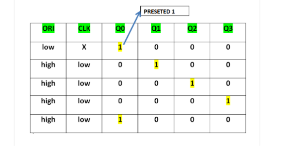
This Preseted 1 is created by setting ORI to zero and setting the time Clock (CLK) to don't care. After that, the ORI was set to high and a low clock pulse signal was applied as the clock (CLK) was triggered on the negative edge. The preset 1 is then transferred to the next flip-flop with each clock pulse, forming Ring.
We can deduce from the above table that the 4-bit Ring Counter has four states.
The following are the four states:
1 0 0 0
0 1 0 0
0 0 1 0
0 0 0 1
Using four D flip-flops, a 4-bit Ring Counter can be created.
Q16) What is Asynchronous and Asynchronous Counter?
A16)
The term asynchronous refers to the lack of synchronisation. Something that is neither present nor absent at the same moment. Asynchronous means regulating the operation time by sending a pulse only when the previous operation is done rather than transmitting it at regular intervals in a computer or telecommunication stream.
Asynchronous Counter
We now know what the term "counter" means and what the term "asynchronous" means. Asynchronous clock input can be used to count an asynchronous counter. Flip-flops can be used to make simple counters. Because the count is dependent on the clock signal, changing state bits are used as the clock signal for succeeding flip-flops in an asynchronous counter. The clock pulse ripples through the counter because the Flip-flops are serially coupled. It's often referred to as a ripple counter because of the ripple clock pulse. An asynchronous counter has a total of 2n - 1 counting states.
Asynchronous Truncated Counter and Decade Counter
Because Asynchronous counters, such as the MOD-16 with a resolution of 4-bit, have a maximum output number, it is also possible to utilise a basic Asynchronous counter in a setup where the counting state is less than the maximum output number. Modulo counters, often known as MOD counters, are one of those counters. The counter is setup in such a way that it resets to zero at a pre-determined value and has truncated sequences.
So, a complete sequence counter counts up to a certain number of resolutions (n-bit Resolution), and a truncated counter counts fewer than the maximum number.
The Asynchronous Truncated Counter can be used with combinational logic to take use of the asynchronous inputs in the flipflop.
The output of the Modulo 16 asynchronous counter can be adjusted with additional logic gates to provide a decade (divided by 10) counter output, which is useful in counting standard decimal values or in arithmetic circuits. Decade Counters are the name for this type of counter.
When the output reaches a decimal value of 10, Decade Counters must be reset to zero.
If we count 0-9 (10 steps) the binary number will be –
Number Count | Binary Number | Decimal Value |
0 | 0000 | 0 |
1 | 0001 | 1 |
2 | 0010 | 2 |
3 | 0011 | 3 |
4 | 0100 | 4 |
5 | 0101 | 5 |
6 | 0110 | 6 |
7 | 0111 | 7 |
8 | 1000 | 8 |
9 | 1001 | 9 |
As a result, the counter must be reset when the output hits 1001 (BCD = 9). We must pass this condition back to the reset input to reset the counter. A BCD or Binary-coded Decimal counter is one that counts from 0000 (BCD = 0) to 1001 (BCD = 9).
Q17) Give Advantages and Disadvantages of Asynchronous Counter.
A17)
Type D flip-flops make it simple to create asynchronous counters. They can be built using a “divide by n” counter circuit, which provides a lot more flexibility for applications that require a huge counting range, and the truncated counter can generate any modulus number count.
Despite these advantages, Asynchronous counter has significant drawbacks and restrictions.
When using the Asynchronous counter, resynchronizing the flipflops necessitates the use of additional re-synchronizing output flip-flops. Additionally, when the truncated sequence count is not equal to, further feedback logic is required.
When counting a large number of bits, the chain system caused the propagation delay between consecutive stages to become excessively significant, making it difficult to eliminate. Synchronous counters are faster and more trustworthy in this case. When high clock frequencies are applied across the Asynchronous Counter, there are additional counting mistakes.
Q18) Explain Different Types of Asynchronous counters.
A18)
There are many types of Asynchronous counters available in digital electronics. They are
- 4 bit synchronous UP counter
- 4 bit synchronous DOWN counter
- 4 bit synchronous UP / DOWN counter
- Asynchronous 4-bit UP counter
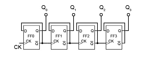
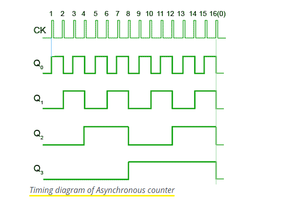
In the diagram above, a 4 bit asynchronous UP counter with D flip flop is depicted. It has the ability to count numerals from 0 to 15. The clock inputs of all flip flops are cascaded, and each flip flop's D input (DATA input) is connected to one of the flip flop's state outputs.
Each active edge or positive edge of the clock signal will toggle the flip flops. The first flip flop is connected to the clock input. The clock signal is input to the other flip flops in the counter via Q' output of the previous flip flop. When the clock signal has a positive edge, the output of the first flip flop will change.
The flip flops in the asynchronous 4-bit up counter are connected in toggle mode, thus if the clock input is connected to the first flip flop FF0, the output after one clock pulse is 20.
The clock input of the next flip flop is triggered by the rising edge of the Q output of each flip flop. It sets the next clock frequency to half of the input frequency. The count of the 4 bit UP counter is represented by the Q outputs of each individual flip flop (Q0, Q1, Q2, Q3) (8).
The operation of an asynchronous up counter is described below.
Assume that the flip flops' four Q outputs are originally set to 0000. When the rising edge of the clock pulse is applied to the FF0, the output Q0 changes to logic 1 and the output Q0 changes to logic 0 with the following clock pulse. This signifies that the clock pulse's output state toggles (from 0 to 1) for one cycle.
Because the clock input of FF1 is connected to the Q' of FF0, the clock input of the second flip flop becomes 1. As a result, the output of FF1 is high (i.e. Q1 = 1), indicating a value of 20. As a result, the following clock pulse will cause Q0 to become high once more.
As a result, both Q0 and Q1 are now high, making the four-bit output 11002. When we apply the fourth clock pulse, it toggles the FF2 and sets the Q0 and Q1 to low states. As a result, the output Q2 will be 00102. Because this is a four-bit up counter, the output is a binary sequence ranging from 0 to 15, or 00002 to 11112. (0 to 1510).
Q19) Write Short note on Synchronous counters.
A19)
The clock inputs of all the various flip-flops within the counter are all clocked simultaneously at the same time by the same clock signal, which is why they're called synchronous counters.
The output of one counter stage is connected directly to the clock input of the next counter stage, and so on, as we saw in the previous Asynchronous binary counter tutorial.
As a result, the Asynchronous counter experiences "Propagation Delay," in which the timing signal is delayed by a fraction as it passes through each flip-flop.
The external clock signal is connected to the clock input of EVERY individual flip-flop within the counter in the Synchronous Counter, causing all of the flip-flops to be clocked together simultaneously (in parallel) at the same time, resulting in a fixed time relationship. To put it another way, changes in the output are “synchronised” with the clock signal.
As a result of this synchronisation, all of the individual output bits change state at the same moment in response to the common clock signal, resulting in no ripple effect and thus no propagation delay.
Q20) Explain Different Types of Synchronous Counters.
A20)
There are many types of synchronous counters available in digital electronics. They are listed below.
- Binary counters
- 4 bit synchronous UP counter
- 4 bit synchronous DOWN counter
- 4 bit synchronous UP / DOWN counter
- Loadable counters
- BCD counters
- Ring counters
- Johnson counters etc.
4 bit Synchronous UP Counter
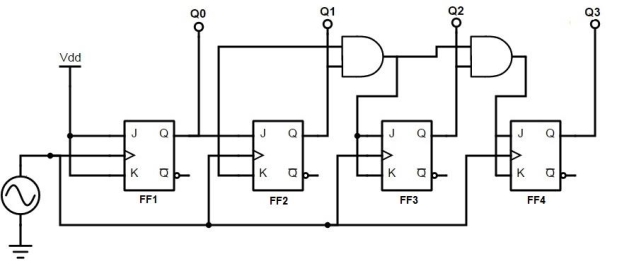
The JK flip flop is used to create the four-bit up counter depicted in the diagram below. All of the flip flops are wired in parallel to an external clock pulse.
JK flip flop is recommended for counter design.
The importance of employing a JK flip flop is that it can toggle its state depending on the clock pulse if both inputs are high.
The first flip flop's inputs are linked to HIGH (logic 1), causing the flip flop to toggle for each clock pulse input. As a result, the synchronous counter will operate with a single clock signal and will change state with each pulse.
4 bit Synchronous DOWN Counter
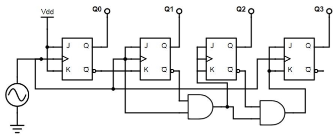
The numbers are counted in decreasing order by the down counter. This is comparable to an up counter, but the count should be reduced. As a result, the inverted Q (Q') is connected to the inputs of the JK flip-flop. The JK flip flop is used to create the four-bit down counter depicted in the diagram below. All of the flip flops are connected to the same external clock pulse.
4 bit Synchronous Up/Down Counter
The two counters mentioned above can be combined into a single counter called up down counter. This can be chosen from the available options. Below is a design for an up/down counter using JK flip flops.
