UNIT 1
- What is a signal?
A signal is a description of how one parameter varies with another parameter.

For example: voltage changing over time in an electronic circuit.

Picture brightness : A camera senses the incoming light and records the light reflectivity as a function of space onto a magnetic film.
2. Explain is filtering?
Filtering is the process of attenuating the unwanted signal or to reproduce the selected portions of the frequency components of a particular signal.
Filters
In the process of shaping a signal, if some portions of the signal are felt unwanted, they can be cut off using a Filter Circuit. A Filter is a circuit that can remove unwanted portions of a signal at its input. The process of reduction in the strength of the signal is also termed as Attenuation.
3. What are the types of filters?
We have four main types of filters −
- Low pass filter
- High pass filter
- Band pass filter
- Band stop filter
Low Pass Filter
A Filter circuit which allows a set of frequencies that are below a specified value can be termed as a Low pass filter. This filter passes the lower frequencies. The circuit diagram of a low pass filter using RC and RL are as shown below.
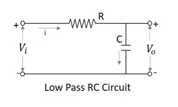
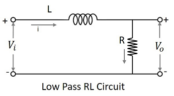
The capacitor filter or RC filter and the inductor filter or RL filter both act as low pass filters.
- The RC filter − As the capacitor is placed in shunt, the AC it allows is grounded. This by passes all the high frequency components while allows DC at the output.
- The RL filter − As the inductor is placed in series, the DC is allowed to the output. The inductor blocks AC which is not allowed at the output.
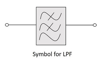
The symbol for a low pass filter LPFLPF is as given below.
4. Explain the frequency response?
The frequency response of a practical filter is as shown here under and the frequency response of an ideal LPF when the practical considerations of electronic components are not considered will be as follows.

The cut off frequency for any filter is the critical frequency fcfc for which the filter is intended to attenuate cutcut the signal. An ideal filter has a perfect cut-off whereas a practical one has few limitations.
5. What is RLC filter?
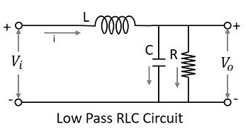
The signal at the input goes through the inductor which blocks AC and allows DC. Now, that output is again passed through the capacitor in shunt, which grounds the remaining AC component if any, present in the signal, allowing DC at the output. Thus, we have a pure DC at the output. This is a better low pass circuit than both of them.
6. Explain the frequency response of RLC filter?
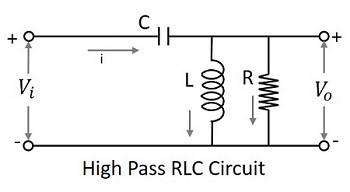
The signal at the input goes through the capacitor which blocks DC and allows AC. Now, that output is again passed through the inductor in shunt, which grounds the remaining DC component if any, present in the signal, allowing AC at the output. Thus, we have a pure AC at the output. This is a better high pass circuit than both of them.
7. What is band pass filter?
A Filter circuit which allows a set of frequencies that are between two specified values can be termed as a Band pass filter. This filter passes a band of frequencies.
As we need to eliminate few of the low and high frequencies, to select a set of specified frequencies, we need to cascade a HPF and a LPF to get a BPF. This can be understood easily even by observing the frequency response curves.
The circuit diagram of a band pass filter is as shown below.
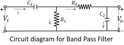
The above circuit can also be constructed using RL circuits or RLC circuits. The above one is a RC circuit chosen for simple understanding.
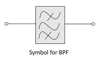
The symbol for a band pass filter BPFBPF is as given below.
8. What are the properties of semiconductor?
Semiconductors can conduct electricity under preferable conditions or circumstances. This unique property makes it an excellent material to conduct electricity in a controlled manner as required.
Unlike conductors, the charge carriers in semiconductors arise only because of external energy (thermal agitation). It causes a certain number of valence electrons to cross the energy gap and jump into the conduction band, leaving an equal amount of unoccupied energy states, i.e. holes. Conduction due to electrons and holes are equally important.
- Resistivity: 10-5 to 106 Ωm
- Conductivity: 105 to 10-6 mho/m
- Temperature coefficient of resistance: Negative
- Current Flow: Due to electrons and holes
9. What are diodes ?
Junction Diode: Principle of Diodes
V Barrier
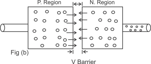
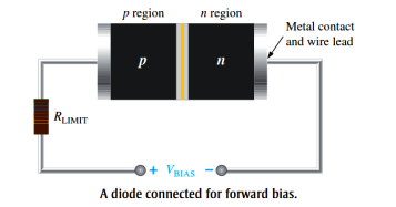
- A Forward biased showing the flow of majority carriers and the voltage due to the barrier potential across the depletion region-
- To bias a diode apply d,c vtg across it .
- Forward bias is the condition that allows current through the PN junction.
- Negative side of VBIAS is connected to the N -region of the diode and the positive side is connected to the P- region.
- A selected requirement is that the bias voltage VBIAS must be greater than the barrier potential.
- Because of like charges repel, the negative side of the bias voltage source pushes the free electrons , which are the majority carriers in the N-region towards the PN junction .the flow of free is called Electron Current.
- The –Ve side of the source also provide a continues flow of electrons through the external connection (conductor).
- Into the N-region as show in fig-B
- The bias voltage source imparts sufficient energy to the free electrons for them to overcome the barrier potential of the depletion region and move on through into the 'p' region once in the P-region. These conduction electrons have lost enough energy to immediately combine with holes in the valence band.
- Now the e- are in the valance band in the P-region simply because they have lost too much energy overcoming the barrier potential to remain in the conduction band. Since unlike charge attract, the positive side of the bias voltage source attracts the valence electrons toward the left end of the region.
- The hole in the P-region provide the medium or "Pathway" for these valence electrons to move through the P-region.
- The holes which are the majority carriers in the P-region, effectively (not actually) move to the right toward the junction as shown in fig-B.
- The defective flow of holes is called the hole current.
- As from Fig-B hole current as the flow of valence electrons through the P-region with the holes providing the only means for these electrons to flow.
- As the electrons flow out of the P-region through the external connection and to the positive side of the bias in the P-region at the same time these electrons become conduction electrons in the mater conductor.
- To these is a continues availability of holes effectively moving towards the PN junction stream of electrons as they come across the junction in to the P-region.
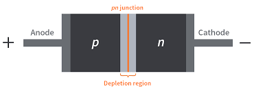
The effect of forward bias on the depletion region:-


+-


 -
-
Depletion Region
- Forward bias narrows the depletion region & produce a vtg drop across pn junction equal to the barrier potential.
- As more electrons flow into the depletion region , the number of positive ions is reduce . As more notes effectively flow into the depletion region on the other side of the pn junction ,the number of -ve ions is reduce this reduction in positive & -ve ions during forward bias causes the depletion region to narrow.
The Effect of the Barrier Potential during forward bias:-
- The electronic field between the positive and negative ions in the depletion region on either side of the junction creates an energy bill, that prevent free R form diffusing across the junction at equilibrium this is known as the barrier potential
- When forward bias is applied the free electrons are provided with enough energy from the bias voltage source to overcome the barrier potential and effectively climb the energy bill and cross the depletion region.
- The energy that the electronics repair in order to pass through the depletion region is equal to the barrier potential.
- Electron gives up an amount of energy equivalent to the barrier potential when they cross the depletion region.
- This energy loss results in a vtg drop across the pn junction equals to the barrier potential (0.7v)
- An additional small vtg drop across the P & N regions due to the internal resistance of the material.
- For doped Semiconductor material, this resistance called the dynamic resistance is very small and can usually be neglected.
10. Explain reverse bias?
REVERSE BIAS:-
Reverse bias is the condition the essentially prevents current through the diode.


P-region N- region


-+
V BIAS
A Diode connected for Reverse Biased-
- Because unlike charges attract the positive side of the bia voltage source pulls the free election, which are the majority carriers in the N-region away from the PN junction.
- AS the election flow towards the positive side of the voltage source additional positive ions are created
- This results in a widening of the depletion region and a depletion of majority carriers.


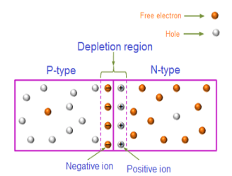
- The diode during the short transition time immediately after reverse bias vtg is applied-
- In the P-region electrons from the negative side of the vtg source enter as valence electron and move from hole to hole toward the depletion region where the creators additional -ve ions.
- This results in a widening of the depletion region and a depletion of majority carriers
- As the depletion region widens the availability of majority carriers decreases
- As more of the N & P regions become depleted of majority carriers, the electric field between the positive and -ve ions increase in strength the depletion region equals the bios vtg .this point the transition current essentially ceases except for a small reverse current that can usually be neglected.
Reverse Current
- Extremely small current that exist in reverse bias after the transition current dies act is caused by the minority carrier in the N& P region that are produced by the manly generated e hole pairs.
- The conduction band in the P-region is at a higher energy level then the conduction band in the N-region. Therefore, the minority easily pass through the depletion region because they required no additional energy.
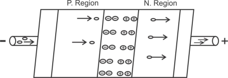
The Extremely small reverse current in a reverse biased diode is due to the minority carriers from thermally generated
e=hole pairs
The Diode - Before doping the p-type & N-type consisting silicon material atom acting as a neutral.
IF a piece of intrinsic silicon is doped so that part is n-type and the other part is p-type, a junction forms at the bounded between the two regions and a diode is created.
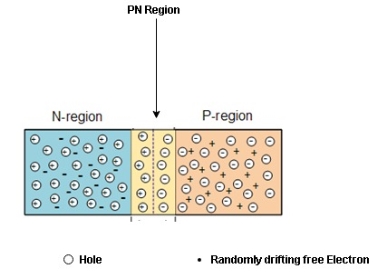
Formation of the Depletion Region
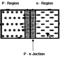
At the instant of junction formation , free electrons in the N-region near the p-n junction being to diffuse across the junction and fall into holes near the junction in the P-region.

For every electron that defuse across the junction and combines with a hole , a positive charge is left in the region and a ve charge is created in the p-region firming a barriers potential. This action continues until the vtg of the barrier ripples further diffusion.
The Depletion region acts as a barriers to the farther movement of electrons across the junction
As positive ion & -ve ion across the junction produces a electric field across the junction -according to coulombs law.
The potential difference of the electric field across the depletion region is the amount of vtg required to move electronics through the electric field, this potential difference is called the barrier potential & is expressed in volt
The typical barrier potential is approximately 0.7 v for silicon & 0.3 v for germanium at 25c.
11. Explain the V-I characteristics of diode ?
V-I characteristics of junction diode
A :- v=A Characteristic for forward bias:-
If (mA)


 C
C

 A B
A B
o 0.7V vf
V-I Characteristics:-
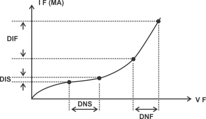
Graph shows how the dynamic resistance decrease as we move up the curve xd= DNF/DIF=
When the forward bias vtg is increased to a value where the vtg across the diode reaches approximately 0.7 v (barrier potential . The forward currant begins to increase rapidly
As we continue to increase the forward bias voltage the current continues to increase very rapidly ,but the voltage across the diode increase only gradually above 0.7 v.
This small increase in the diode vtg above the barrier potential is due to the voltage drop across the internal dynamic resistance of the semi conductive material.
Dynamic resistance:- A Resistance change as move along a V-I curve it is called dynamic or A. C resistance.
|
12. Explain the diode current equation?
Diode Current Equation
 ampers
Where ,
V= Applied voltage across the diode in volts
I=Current flow through the diode in amperes.
n= 2 for silicon P-N junction diode
=1 for germanium P-N junction diode.
IO = reverse saturation current flow through diode in amperes.
VT =Is the voltage equivalent of temperature in volts.
VT= K X T volt’s
K=Boltzmann's constant
K=8.62 * 10 -s ev/k
I= temperature in ok
The equation VI= K * T indicates that the current flow through the diode also depend upon the ambient temperature.
Room temperature =25 0c
T= 273+25=298K
VT=K * T


13. Explain equivalent circuit of diode ?
Equivalent circuit of Diode

Breakdown Mechanism
i) Avalanche breakdown:-As the magnitude of the reverse bias vtg is increased the kinetic energy of the minority carriers gets increased. While travelling the minority carriers collide with the stationery atoms which in turns results in breaking some of the covalent bond & generating free e- (carrier multiplication)
This process continues leading to a very swift multiplication giving rise to a large reverse current in just a few picoseconds. This effect is called as avalanche breakdown effect.
Topical Breakdown vtg is about 50v to 100v:-
i) Due to large power dissipation the junction temperature increase & may destroy the semiconductor device permanently.
Ii) Zener Breakdown: - This type of breakdown occurs in heavily doped P-N junction in which the depletion region is very narrow.
All the applied reverse voltage appears across the depletion layer. The electric field is vtg per unit distance. It is very intense at the depletion region.
There for it can pull the electronic out of the valance bond by breaking the covalent bonds and producing the free electrons. This process is known as zener effect.
Due to this heavy current flow & diode may damage.
14. Explain Zener diode ?
Zener Diode
- Zener diode is a special type of p-n junction semiconductor diode in this diode the reverse breakdown voltage is adjusted precisely between 3v to 200v.
- Its applications are based on this principle hence Zener diode is called as a breakdown diode.
- The doping level of the imparity added to manufacture the zener diode is controlled in order to adjust the precise value of breakdown voltage.
PRINCIPLE OF OPERATION: - A zener diode can be forward biased or reverses biased. Its operation in the forward biased mode is same as that of a p-n junction diode but its operation in the reverse biased mode is sustainably deferent.

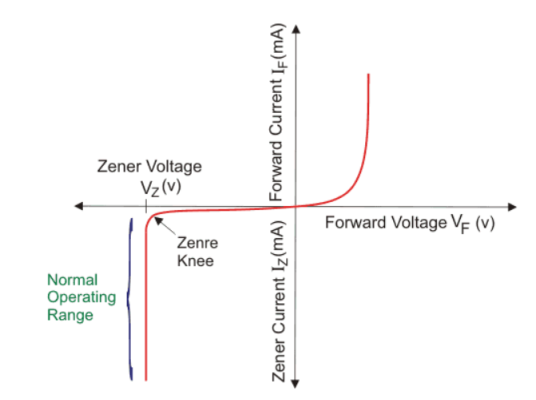
15. A 5.0V stabilized power supply is required to be produced from a 12V DC power supply input source. The maximum power rating PZ of the zener diode is 2W. Using the zener regulator circuit above calculate:
a). The maximum current flowing through the zener diode.
Maximum current = Watts/ Voltage =2W/5V =400mA
b). The minimum value of the series resistor, RS
 = 17.5 Ω
c). The load current IL if a load resistor of 1kΩ is connected across the zener diode.

d). The zener current IZ at full load.
Iz =Is -Il =440mA – 5mA = 395mA
