MICRO
UNIT - 6Hardware Specifications, Memory Interface – 1 Q1) Explain to functions of pin 25 and 24 of 8086?A1) INTA is an interrupt acknowledgement signal and is present at pin 24. When the microprocessor receives this signal, it acknowledges the interrupt. ALE stands for address latch enable and is available at pin 25. A positive pulse is generated each time the processor begins any operation. This signal indicates the availability of address on the address/data lines. The queue status signals are present at pin 24 and 25. They provide the status of instruction queue and their conditions are–
Q2) Explain the pin functions of pins 26-30 of 8086?A2) DE stands for Data Enable and is available at pin 26. It is used to enable Transreceiver 8286. DT/R stands for Data Transmit/Receive signal and is present at pin 27. It decides the direction of data flow with the help of the transreceiver. When it is high, data is transmitted and vice-a-versa. M/IO is used to distinguish between memory and I/O operations. When it is high, it indicates I/O operation and when low it indicates the memory operation. It is present at pin 28. WR stands for write signal and is present at pin 29. It is used for writing the data into the memory or the output device depending on the status of M/IO signal. HLDA stands for Hold Acknowledgement signal and is present at pin 30. This signal acknowledges the HOLD signal. Q3) Explain about the status signals used by bus controller to generate memory and I/O control signals?A3) They are the status signals that provides the status of operation used by the Bus Controller 8288 to generate memory & I/O control signals. These are present at pin 26, 27, and 28.
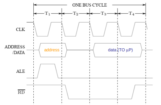
Q4) Explain the bus timing diagram for read cycle?A4) 8086 and 8088 bus cycles consume four system clock periods (T-states), T1, T2, T3 and T4. At 5MHz, each T-state is 200nS, therefore a bus cycle is 800nS. Semi-synchronous bus control allows inserting of wait states (Tw), also 200nS, between T3 and T4 which allows access to slow memory and I/O devices. Most processors are very similar in I/O and memory access operations.
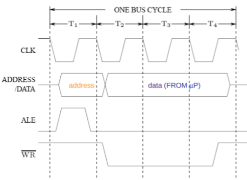
Fig 1 Read CycleT1: Address, ALE, DT/R, M/IO. T2: RD, WR, DEN, data on the bus (for write). At the end of T2 (middle of T3), µP samples READYT3 /Tw: Gives time for memory or I/O device to read/write.For read cycles, data bus is sampled at end of T3.T4: All bus signals are deactivated. Q5) Draw timing diagram of write cycle?A5)
Fig 2 Write CycleT1: Address, ALE, DT/R, M/IO. T2: RD, WR, DEN, data on the bus (for write). At the end of T2 (middle of T3), µP samples READYT3 /Tw: Gives time for memory or I/O device to read/write. Q6) Draw and explain wait state generation circuit?A6)
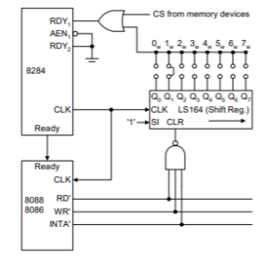
Fig 3 Wait State Generation Circuit
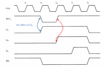
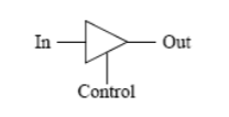
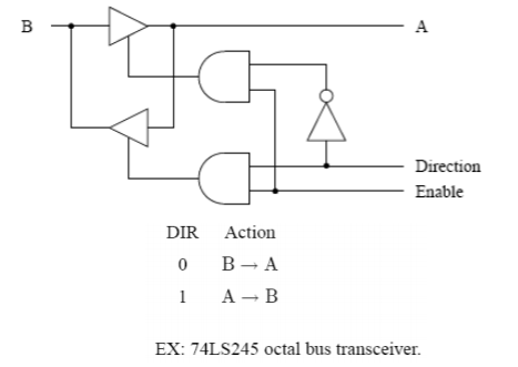
Fig 4 Wait State Generation Timing Diagram Wait state (TW): It is an extra clocking period, inserted between T2 & T3 in order to give memory and other slow devices to complete data transfer. READY input: This input causes wait states for slower memory & I/O components. Q7) Explain the minimum and maximum mode of 8086?A7) 8086 microprocessor operates in 2 modes:Minimum mode It can be selected by setting MN/MX pin to logic 1 and it acts like a single microprocessor. In this mode, all the control signals are provided by the microprocessor chip itself. Maximum modeThis operation can be selected by setting MN/MX pin to logic 0 and microprocessor acts like a multiprocessor. It provides the signals for implementing a multi core processor system environment and in this each processor executes its own program. In this type of system environment, some system resources that are common to all processors are present. They are known as global resources. Co-processor means there is a second processor in the system, but both of them cannot access the system bus at the same time. One processor passes the control of the system bus to the other & then can also suspend its operation. Q8) What are latches and how they are used to de-multiplex the address/data and address/status lines?A8) Latches are used to de-multiplex the address/data and address/status lines and commonly have output buffers for driving external loads. Buffers are used to drive external loads, and to isolate component when disabled.
Fig 5 Latches for various purposeWhen enabled by the control line, output follows input (buffered, pass-through). When disabled, output is a very high impedance which prevents the output from driving or loading connected circuits. When disabled, the outputs are said to be floating. It is like a switch.
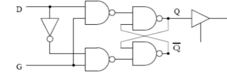
Fig 6 LatchesWhen enable is high, Q follows D. • When enable goes low, Q maintains (latches) state of D. Q9) Draw pin diagram of 8086 and explain about the address and data bus?A9)
Fig 7: Pin DiagramAD0-AD15 are 16 address/data bus. AD0-AD7 carries lower order data byte and AD8-AD15 carries higher order data byte. A16-A19/S3-S6 are the 4 address/status buses. During the first clock cycle, they carry 4-bit address and then carries status signals. BHE stands for Bus High Enable. It is present at pin 34 and used to indicate the transfer of data using data bus D8-D15. This is low signal present during the first clock cycle and thereafter it is active.
QS0 | QS1 | Status |
0 | 0 | No operation |
0 | 1 | First byte of opcode from the queue |
1 | 0 | Empty the queue |
1 | 1 | Subsequent byte from the queue |
S2 | S1 | S0 | Status |
0 | 0 | 0 | Interrupt acknowledgement |
0 | 0 | 1 | I/O Read |
0 | 1 | 0 | I/O Write |
0 | 1 | 1 | Halt |
1 | 0 | 0 | Opcode fetch |
1 | 0 | 1 | Memory read |
1 | 1 | 0 | Memory write |
1 | 1 | 1 | Passive |
|
|
|
|
|
|
|
0 matching results found
